

Intersil Corporation HI7188 Datasheet

August 1997
HI7188
8-Channel, 16-Bit, High Precision,
Sigma-Delta A/D Sub-System
Features
• Fully Differential 8-Channel Multiplexer and Reference
• Automatic Channel Switching with Zero Latency
• 240 Conversions Per Second Per Channel
• 16-Bit Resolution with No Missing Codes
• 0.0015% Integral Non-Linearity
• Fully Software Configurable
- -120dB Rejection of 60/50Hz Line Noise
- Channel Conversion Order and Number of Active
Channels
- True Bipolar or Unipolar Input Range Per Channel
- PGIA Gain Per Channel
- 2-Wire or 3-Wire Interface
• Chopper Stabilized PGIA with Gains of 1 to 8
• Serial Data I/O Interface, SPI Compatible
• 3 Point System Calibration
• Low Power Dissipation of 30mW (Typ)
Applications
• Multi-Channel Industrial Process Controls
• Weight Scales
• Medical Patient Monitoring
• Laboratory Instrumentation
• Gas Monitoring System
• Reference Literature
- AN9504 “A Brief Introduction to Sigma Delta
Conversion”
- TB329 “Intersil Sigma-Delta Calibration Techniques”
- AN9518 “Using the HI7188 Evaluation Kit”
- AN9610 “Interfacing the HI7188 to a Microcontroller”
- AN9538 “Using the HI7188 Serial Interface”
Ordering Information
PART
NUMBER
TEMP.
RANGE (oC) PACKAGE PKG. NO.
Description
The HI7188 is an easy-to-use 8-Channel sigma-delta programmable A/D subsystem ideal for low frequency physical
and electrical measurements in scientific, medical, and
industrial applications. The subsystem has complete on-chip
capabilities to support moving the intelligence from the system controller and towards the sensors. This gives the
designer faster and more flexible configurability without the
traditional drawbacks of low throughput per channel, higher
power or cost per channel. Extreme design complexity and
excessive software overhead is eliminated.
The HI7188 contains a fully differential 8 channel multiplexer,
Programmable Gain Instrumentation Amplifier (PGIA), 4th
order sigma-delta ADC, integrating filter, line noise rejection
filters, calibration and data RAMs, clock oscillator, and a
microsequencer. Communication with the HI7188 is performed via the serial I/O port, and is compatible with most
synchronous transfer formats, including both the Motorola/Intersil 6805/11 series SPI, QSPI and Intel 8051 series
SSR protocols.
The powerful on-board microsequencer provides automatic
conversions on the multiplexed input channels (up to 8) by
controlling all channel switching, filtering and calibration. The
microsequencer supports on-the-fly multiplexer reconfiguration, forty to fifty times faster throughput than the competition
and zero step response delay during internal or external
multiplexer channel changes. A simple set of commands
gives the user control over calibration, PGIA gain, and bipolar/unipolar modes on a per channel basis. Number of channels to convert, data coding, line noise rejection, etc. is
programmed at the chip level. The calibration RAMs allow
the user to read and write system calibration data while the
data RAMs provide a read support of the conversion results
for each channel.
This design is effectively eight 16-bit (for 96dB noise-free
dynamic range) Sigma-Delta A/D converters combined with
a microsequencer and an eight-channel multiplexer in a single package. The HI7188 provides 120dB line-noise rejection at 240 samples/second/channel (in 60Hz line-rejection
mode) and 200 samples/second/channel (in 50Hz line-rejection mode) base output data rates. By reusing multiplexer
channels for the same input, throughput can increase by
integer increments of the base output data rate up to
1920Hz.
HI7188IP -40 to 85 40 Ld PDIP E40.6
HI7188IN -40 to 85 44 Ld MQFP Q44.10x10
HI7188EVAL 25 Evaluation Kit
CAUTION: These devices are sensitive to electrostatic discharge; follow proper IC Handling Procedures.
http://www.intersil.com or 407-727-9207
| Copyright © Intersil Corporation 1999
7-1847
File Number 4016.4
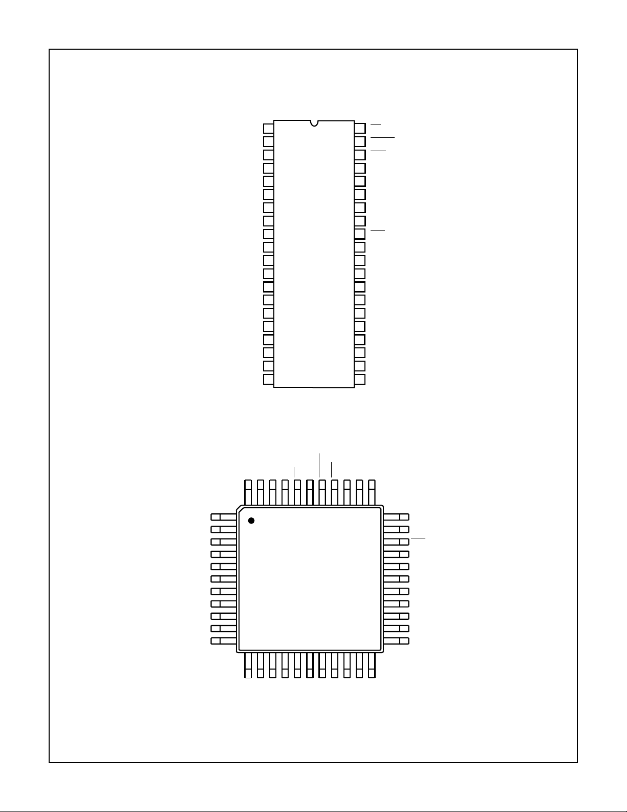
Pinouts
HI7188
HI7188 (PDIP)
TOP VIEW
MODE
SCLK
SDO
SDIO
OSC
OSC
DV
DD
DGND
AV
V
INL1
V
INH1
V
INL2
V
INH2
V
INL3
V
INH3
V
INL4
V
INH4
V
INL5
V
INH5
V
INL6
SS
1
2
3
4
5
1
6
2
7
8
9
10
11
12
13
14
15
16
17
18
19
20
40
39
38
37
36
35
34
33
32
31
30
29
28
27
26
25
24
23
22
21
CS
RSTI/O
EOS
A
2
A
1
A
0
MXC
CA
RST
DGND
AV
SS
AV
DD
V
RHI
V
RLO
V
CM
V
INH8
V
INL8
V
INH7
V
INL7
V
INH6
HI7188 (MQFP)
TOP VIEW
OSC
OSC
DV
DD
DGND
AV
AV
V
INL1
V
INH1
V
INL2
V
INH2
V
INL3
SS
SS
DGND
RSTI/O
SDIO
SDO
SCLK
MODE
CS
44 43 42 41 40
1
2
1
2
39 38 37 36 35 34
EOS
3
4
5
6
7
8
9
10
11
12 13 14 15 16 17
INL4
INL5
INL6
INH3
V
INH4
V
INH5
V
V
V
INL7
INH6
V
V
V
A2A1A
33
32
31
30
29
28
27
26
25
24
23
2221201918
INL8
INH7
V
V
0
INH8
V
MXC
CA
RST
DV
DD
DGND
AV
SS
AV
SS
AV
DD
V
RHI
V
RLO
V
CM
7-1848

HI7188
OSC1
OSC2
CH1
CH2
CH1
REGISTERS
CALIBRATION
AND CONTROL
CH2
CH2
RAM0 RAM1
16
CH1
LNR
BYPASS
LINE NOISE FILTER
CH3
CH3
CH3
24
CH4
CH4
CH4
CH5
CH5
CH5
CH6
CH6
CH6
CH7
CH7
CH7
CH8
CH8
CH8
CLOCK
SERIAL
INTERFACE
CONTROL
GENERATOR
REGISTER
CAEOS MODE CSRST RSTIOSDIOSDOSCLK
16
24
CONVERSION CONTROL
Functional Block Diagram
RLO
V
RHI
V
CM
V
LOGICAL
CHANNELS
PHYSICAL
CHANNELS
IN1HVIN2HVIN3HVIN4HVIN5HVIN6HVIN7HVIN8H
V
CH1
CH2
CH3
INTEGRATING
FILTER
1
4TH
ORDER
CH4
CH5
23
∑ − ∆
MODULATOR
PGIA
IN1LVIN2LVIN3LVIN4LVIN5LVIN6LVIN7L
V
CH6
PGIA GAIN
CH7
CH8
MODE
CHANNEL SELECT
BIPOLAR/UNIPOLAR
IN8L
V
LOGICAL
1
A0A2A
LOGICAL SEQUENCER
ADDRESS
CHANNEL
MXC
CCR REGISTERS
7-1849

Typical Application Schematic
HI7188
3.6864MHz
CHANNEL 1
CHANNEL 2
CHANNEL 3
CHANNEL 4
CHANNEL 5
CHANNEL 6
CHANNEL 7
CHANNEL 8
AV
V
V
V
V
V
V
V
V
V
V
V
V
V
V
V
V
V
V
V
AV
DD
RHI
RLO
INH1
INL1
INH2
INL2
INH3
INL3
INH4
INL4
INH5
INL5
INH6
INL6
INH7
INL7
INH8
INL8
CM
SS
17 16
OSC
OSC
1
HI7188IP
8, 31
DV
2
SCLK
SDIO
SDO
RSTI/O
EOS
RST
MXC
MODE
DGND
CS
CA
A
A
A
DD
4.7µF
+5V
DATA I/O
DATA OUT
RSTI/O
CS
EOS
CA
RST
MXC
A
2
A
1
A
0
+
0.1µF
2
4
3
39
40
38
33
32
34
37
2
36
1
35
0
1
+5V
0.1µF
R
1
+2.5V
REFERENCE
+
-
+
-
+
-
+
-
+
-
+
-
+
-
+
-
-5V
0.1µF 4.7µF
+
29
+
4.7µF
28
27
11
10
13
12
15
14
17
16
18
17
21
20
23
22
25
24
26
9, 30
+
7-1850
Pin Descriptions
HI7188
40 LEAD
PDIP
44 LEAD
MQFP PIN NAME PIN DESCRIPTION
1 41 MODE Mode input. Used to select between Synchronous Self Clocking (MODE = 1) or Synchronous Ex-
ternal Clocking (MODE = 0) for the Serial Port.
2 42 SCLK Serial interface clock. Synchroniz es serial data transfers . Data is input on the rising edge and out-
put on the falling edge.
3 43 SDO Serial Data Out. Serial data is read from this line when using a 3-wire serial protocol such as the
Motorola Serial Peripheral Interface.
4 44 SDIO Serial Data IN or OUT. This line is bidirectional programmable and interfaces directly to the Intel
Standard Serial Interface using a 2-wire serial protocol.
5 1 OSC
Oscillator clock input for the device . A crystal connected between OSC1and OSC2will provide a
1
clock to the device, or an external oscillator can drive OSC1. The oscillator frequency should be
3.6864MHz to maintain Line Noise Rejection.
6 2 OSC
7 3, 30 DV
Used to connect a crystal source between OSC1 and OSC2. Leave open otherwise.
2
Positive Digital supply (+5V).
DD
8, 31 4, 29, 39 DGND Digital supply ground.
9, 30 5, 6, 27, 28 AV
10 7 V
11 8 V
12 9 V
13 10 V
14 11 V
15 12 V
16 13 V
17 14 V
18 15 V
19 16 V
20 17 V
21 18 V
22 19 V
23 20 V
24 21 V
25 22 V
26 23 V
27 24 V
28 25 V
29 26 AV
INL1
INH1
INL2
INH2
INL3
INH3
INL4
INH4
INL5
INH5
INL6
INH6
INL7
INH7
INL8
INH8
RLO
Negative analog power supply (-5V).
SS
Analog input low for Channel 1.
Analog input high for Channel 1.
Analog input low for Channel 2.
Analog input high for Channel 2.
Analog input low for Channel 3.
Analog input high for Channel 3.
Analog input low for Channel 4.
Analog input high for Channel 4.
Analog input low for Channel 5.
Analog input high for Channel 5.
Analog input low for Channel 6.
Analog input high for Channel 6.
Analog input low for Channel 7.
Analog input high for Channel 7.
Analog input low for Channel 8.
Analog input high for Channel 8.
Common mode voltage. Must be tied to the mid point of AVDD and AVSS.
CM
External reference input. Should be negative referenced to V
External reference input. Should be positive referenced to V
RHI
Positive analog power supply (+5V).
DD
RHI
RLO
.
.
32 31 RST Active low Reset pin. Used to initialize modulator, filter, RAMs, registers and state machines.
33 32 CA Calibration active output. Indicates that at least one active channel is in a calibration mode.
34 33 MXC Multiplexer control output. Indicates that the conversion for the activ e channel is complete.
35 34 A
36 35 A
37 36 A
Logical channel count output (LSB).
0
Logical channel count output.
1
Logical channel count output (MSB).
2
38 37 EOS End of scan output. Signals the end of a channel scan (all active channels have been converted)
and data is available to be read. Remains low until data RAM is read.
39 38 RSTI/O I/O reset (active low) input. Resets serial interface state machine only.
40 40 CS Active low chip select pin. Used to select a serial data transfer cycle. When high the SDO and
SDIO pins are three-state.
7-1851

HI7188
Absolute Maximum Ratings Thermal Information
Supply Voltage
AVDD to AVSS. . . . . . . . . . . . . . . . . . . . . . . . . . . . . . . . . . . . . 11V
DVDD to DGND. . . . . . . . . . . . . . . . . . . . . . . . . . . . . . . . . . .+5.5V
Analog Input Pins . . . . . . . . . . . . . . . . . . . . . . . . . . . .AVSS to AV
Digital Input, Output and I/O Pins. . . . . . . . . . . . . . . DGND to DV
ESD Tolerance (No Damage)
Human Body Model . . . . . . . . . . . . . . . . . . . . . . . . . . . . . . . 500V
Machine Model . . . . . . . . . . . . . . . . . . . . . . . . . . . . . . . . . . . 100V
Charged Device Model . . . . . . . . . . . . . . . . . . . . . . . . . . . . . 500V
Operating Conditions
Operating Temperature Range. . . . . . . . . . . . . . . . . . -40oC to 85oC
CAUTION: Stresses above those listed in “Absolute Maximum Ratings” may cause permanent damage to the device. This is a stress only rating and operation
of the device at these or any other conditions above those indicated in the operational sections of this specification is not implied.
NOTE:
1. θJA is measured with the component mounted on an evaluation PC board in free air.
Thermal Resistance (Typical, Note 1) θJA(oC/W)
PDIP . . . . . . . . . . . . . . . . . . . . . . . . . . . . . . . . . . . . 50
MQFP . . . . . . . . . . . . . . . . . . . . . . . . . . . . . . . . . . . 80
DD
Maximum Storage Temperature Range . . . . . . . . . .-65oC to 150oC
DD
Maximum Junction Temperature. . . . . . . . . . . . . . . . . . . . . . . 150oC
Maximum Lead Temperature (Soldering 10s). . . . . . . . . . . . . 300oC
(MQFP - Lead Tips Only)
Electrical Specifications AV
= +5V, AVSS= -5V, DVDD= +5V, V
DD
= +2.5V, V
RHI
= AGND, VCM = AGND, PGIA Gain = 1,
RLO
OSCIN= 3.6864MHz, Bipolar Input Range Selected
o
-40
C TO 85oC
PARAMETER TEST CONDITION
UNITSMIN TYP MAX
SYSTEM PERFORMANCE
Resolution Dependent on Gain (Note 2) - - 16 Bits
Integral Non-Linearity, INL FS = 25Hz, +FS, +MS, 0, -MS, -FS
- ±0.0015 ±0.0045 %FS
End Point Line Method (Notes 3, 5, 6)
Differential Non-Linearity (Note 2) No Missing Codes to 16-Bits Offset Error, VOS (Calibrated) V
Full Scale Error, FSE (Calibrated) V
Gain Error (Calibrated) Slope = +Full Scale - (-Full Scale)
INHI
INHI
= V
- V
(Notes 3, 4) - ±0.0015 - %FS
INLO
= +2.5V (Notes 3, 4) - ±0.0015 - %FS
INLO
- ±0.0015 - %FS
(Notes 3, 4)
Noise, V
N(P-P)
Common Mode Rejection Ratio,
VCM = 0V (Note 5) Delta VCM = ±3V - -75 - dB
- 1/4 - LSB
CMRR
Off Channel Isolation (Note 2) -120 - - dB
ANALOG INPUT
Common Mode Input Range, V
Input Leakage Current, I
Input Capacitance, C
IN
IN
CM
(Note 2) AV
SS
-AVDDVIN = AVDD (Note 3) - - 1.0 nA
(Note 2) See Table 2 - 4.0 pF
DIGITAL INPUTS
Input Logic High Voltage, V
Input Logic Low Voltage, V
Input Logic Current, I
Input Capacitance, C
I
IN
IH
IL
VIN = 0V, +5V - 1.0 10 µA
VIN = 0V (Note 2) - 5.0 - pF
2.0 - - V
- - 0.8 V
DIGITAL CMOS OUTPUTS
Output Logic High Voltage, V
Output Logic Low Voltage, V
OH
OL
I
= -100µA (Note 7) 2.4 - - V
OUT
I
= 3.2mA (Note 7) - - 0.4 V
OUT
7-1852

HI7188
Electrical Specifications AV
= +5V, AVSS= -5V, DVDD= +5V, V
DD
= +2.5V, V
RHI
= AGND, VCM = AGND, PGIA Gain = 1,
RLO
OSCIN= 3.6864MHz, Bipolar Input Range Selected (Continued)
o
C TO 85oC
-40
PARAMETER TEST CONDITION
Output Three-State Leakage
Current, I
OZ
Digital Output Capacitance, C
OUT
V
= 0V, +5V (Note 7) - 1 10 µA
OUT
(Note 2) - 10 - pF
UNITSMIN TYP MAX
TIMING CHARACTERISTICS
SCLK Minimum Cycle Time, t
SCLK Minimum Pulse Width, t
CS to SCLK Precharge Time, t
SCLK
SCLKPW
PRE
Data Setup to SCLK Rising Edge
(Write), t
DSU
Data Hold from SCLK Rising Edge
(Write), t
DHLD
Data Read Access from Instruction
Byte Write, t
ACC
Read Bit Valid from SCLK Falling
Edge, t
DV
Last Data Transfer to Data Ready
Inactive, t
RESET Low Pulse Width t
RSTI/O Low Pulse Width t
MUX High Pulse Width t
DRDY
RESET
RSTI/O
MUX
(Notes 2, 7) 200 - - ns
(Notes 2, 7) 60 - - ns
(Notes 2, 7) 50 - - ns
(Notes 2, 7) 50 - - ns
(Notes 2, 7) 0 - - ns
(Notes 2, 7) - - 40 ns
(Notes 2, 7) - - 40 ns
(Notes 2, 7) - 50 - ns
(Notes 2, 7) 100 - - ns
(Notes 2, 7) 100 - - ns
(Notes 2, 7) 14 µs
CADDR Valid to MUX High (Notes 2, 7) 75 ns
Oscillator Clock Frequency (Notes 2, 7) - 3.6864 - MHz
Output Rise/Fall Time (Notes 2, 7) - - 30 ns
Input Rise/Fall Time (Notes 2, 7) - - 1 µs
POWER SUPPLY CHARACTERISTICS
IAV
DD
IAV
SS
IDV
DD
Power Dissipation, Active PD
A
AVDD = +5V, OSC1 = 3.6864MHz (Note 3) - 1.8 3.0 mA
AVSS = -5V, OSC1 = 3.6864MHz (Note 3) - 1.8 3.0 mA
DVDD = +5V, SCLK = 4MHz - 2.0 4.0 mA
AVDD = +5V, AVSS = -5V, SLP = ‘0’
-2850mW
(Notes 3, 9)
Power Dissipation, Sleep PD
S
AVDD = +5V, AVSS = -5V, SLP = ‘1’
-5-mW
(Notes 3, 9)
PSRR (∆ V
= 0.25V) PSRR = 20log (∆V
supply
/ ∆VOS) (Note 3) - 75 - dB
supply
NOTES:
2. Parameter guaranteed by design or characterization, not production tested.
3. DC PSRR is measured on all supplies individually and applies to both Bipolar and Unipolar Input Ranges.
4. These errors can be removed by re-calibrating at the desired operating temperature.
5. Applies after system calibration.
6. Fully differential input signal source is used.
7. See Load Test Circuit, Figure 1, R1 = 10kΩ, CL = 50pF (Includes Stray and Jig Capacitance).
8. For Line Noise Rejection, 3.6864MHz is required to develop internal clocks to reject 50/60Hz.
9. SLP is the sleep mode enable bit defined in bit 3 of the Control Register (CR <3>).
7-1853
 Loading...