HI-7159A
Data Sheet January 1999 File Number 2936.4
Microprocessor-Compatible, 5-1/2Digit
A/D Converter
The Intersil HI-7159A is a monolithic A/D converter that uses
a unique dual slope technique which allows it to resolve input
changes as small as 1 part in 200,000 (10µV) without the use
of critical external components. Its digital autozeroing feature
virtually eliminates zero drift over temperature. The device is
fabricated in Intersil’ proprietary low noise BiMOS process,
resulting in exceptional linearity and noise performance. The
HI-7159A’s resolution can be s witched betw een a high
resolution 200,000 count (5
20,000 count (4
1
/2 digit) mode without any hardware
modifications. In the 4
1
/2 digit) mode, and a high speed
1
/2digit uncompensated mode, speeds
of 60 conv ersionsper second can be achieved.The HI-7159A
is designed to be easily interfaced with most microprocessors
through either of its three serial and one parallel interface
modes. In the serial modes, any one of four common baud
rates is availab le .
Ordering Information
TEMP.
PART NUMBER
RANGE (oC) PACKAGE
HI3-7159A-5 0 to 70 28 Ld PDIP E28.6
PKG.
NO.
Features
• ±200,000 Count A/D Converter
• 2V Full Scale Reading With 10µV Resolution
1
• 15 Conversions Per Second in 5
• 60 Conversions Per Second in 4
/2 Digit Mode
1
/2 Digit Mode
• Serial or Parallel Interface Modes
• Four Selectable Baud Rates
• Differential Analog Input
• Differential Reference Input
• Digital Autozero
Applications
• Weigh Scales
• Part Counting Scales
• Laboratory Instruments
• Process Control/Monitoring
• Energy Management
• Seismic Monitoring
Pinout
V
CC
INT OUT
INT IN
BUF OUT
C
REF-
GUARD
C
REF-
C
REF+
C
REF+
GUARD
V
HI
REF
LO
V
REF
A
GND
VIN HI
LO
V
IN
V
EE
1
2
3
4
5
6
7
8
9
10
11
12
13
14
HI-7159A
(PDIP)
TOP VIEW
28
27
26
25
24
23
22
21
20
19
18
17
16
15
SEL
X
TAL
D
GND
P7/BRS1
P6/BRS0
P5/SAD3
P4/SAD2
P3/SAD1
P2/SAD0
P1/SMS1
P0/SMS0
CS/SAD4
WR/TXD
RD/RXD
Functional Block Diagram
A
V
GND
EE
INTEGRATOR
-
+
BUFFER
ANALOG SWITCHES
COMPARATOR
+
-
+
-
V
REF HI
V
REF LO
V
V
C
C
INT
R
INT
IN HI
IN LO
REF
V
CC
X
CONTROL
SECTION
AND
LATCHES
ANALOG
STATE
MACHINE
TAL
D
GND
BUS
INTERFACE
UNIT
UART
I/O PORTS
8 BIT
BUS
CS
WR
RD
SEL
1
CAUTION: These devices are sensitive to electrostatic discharge; follow proper IC Handling Procedures.
1-888-INTERSIL or 321-724-7143
| Copyright © Intersil Corporation 1999

HI-7159A
Absolute Maximum Ratings Thermal Information
Supply Voltage
VCC to GND (A
VEE to GND (A
GND/DGND
GND/DGND
Digital Pins, (pins 15 - 28) . . . . . . . . D
) . . . . . . . . . . . . . . -0.3V < VCC < +6V
) . . . . . . . . . . . . . . +0.3V < VCC < -6V
-0.3V < VD <VCC +0.3V
GND
Analog Pins, (pins 2 - 13). . . . . . . . . . .VEE -0.3V < VA < VCC +0.3V
Operating Conditions
Temperature Range. . . . . . . . . . . . . . . . . . . . . . . . . . . 0oC to 70oC
CAUTION: Stresses above those listed in “Absolute Maximum Ratings” may cause permanent damage to the device. This is a stress only rating and operation of the
device at these or any other conditions above those indicated in the operational sections of this specification is not implied.
NOTE:
1. θJA is measured with the component mounted on an evaluation PC board in free air.
Thermal Resistance (Typical, Note 1) θJA (oC/W)
PDIP Package . . . . . . . . . . . . . . . . . . . . . . . . . . . . . 50
Maximum Junction Temperature . . . . . . . . . . . . . . . . . . . . . . 150oC
Maximum Storage Temperature, T
. . . . . . . . . . -65oC to 150oC
STG
Maximum Lead Temperature (Soldering 10s) . . . . . . . . . . . . 300oC
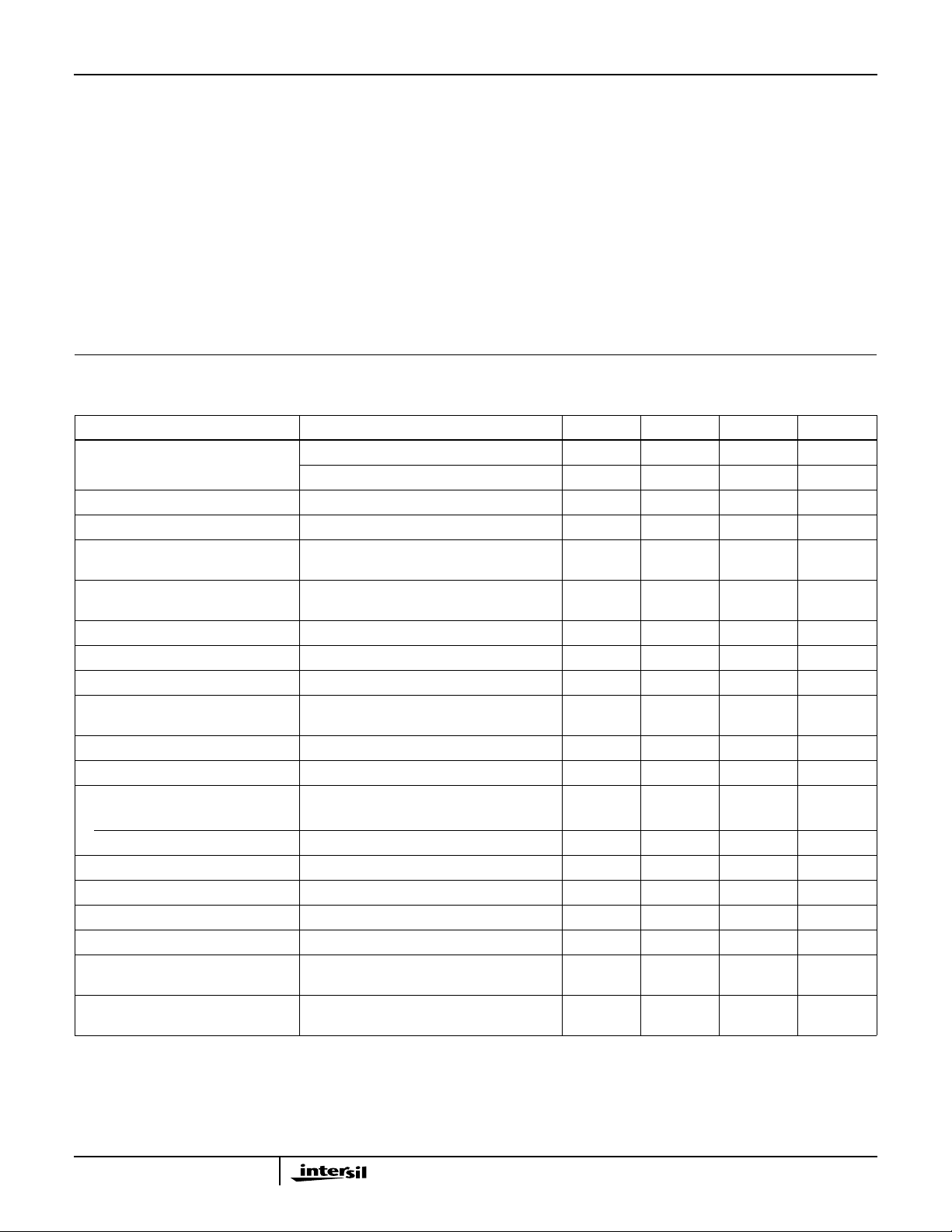
Electrical Specifications Test Conditions: V
= 2.40MHz, R
f
CLOCK
Compensated Mode, Unless Otherwise Specified
= +5V, VEE = -5V, D
CC
= 400kΩ, C
INT
= 0V, A
GND
= 0.01µF, TA = 25oC, V
INT
GND
= 0V, V
IN LO
= +1.00000V, V
REF HI
= A
GND
, C
= 1.0µF, 51/2 Digit
REF
REF LO
= AGND,
PARAMETER TEST CONDITIONS MIN TYP MAX UNITS
Integral Non-Linearity, INL 0V to +2V (Notes 2, 3, 4, 5) - ±0.0015 ±0.0035 % FS
-2V to 0V (Notes 2, 3, 4, 5) - ±0.0015 ±0.0035 % FS
Ratiometric Reading V
Zero Error, ZE V
Voltage Range of V
(Pin 13), V
IN LO
Voltage Range of V
(Pin 12), V
IN HI
IN LO
IN HI
Input
Input
Common Mode Rejection, CMR V
Input Leakage Current, I
Input Capacitance, C
IN
IN
Noise (Peak-to-Peak Value, Not
Exceeded 95% of Time), e
Zero Drift, T
C(ZE)
Full Scale Error Tempco, T
Supply Range, V
V
CC
V
EE
SUPPLY
VCC Supply Current, I
VEE Supply Current, I
Digital GND Current, I
Analog GND Current, I
N
C(FSE)
CC
EE
DGND
AGND
VCC, VEE Power Supply Rejection,
PSR
Guard Driver Pins 5, 8
Output Current, I
OGD
= V
IN HI
= 0.00000V - 0 ±1 Counts
IN HI
-2V ≤ V
IN HI
-2V ≤ V
IN HI
= V
IN HI
= 1.00000V 99996 100000 100003 Counts
REF HI
- V
- V
IN LO
≤ 2V -1 - 1 V
IN LO
≤ 2V V
IN LO
-2V - V
IN LO
+2V V
IN LO
= -3V to +3V - 3 - Counts
Pins 9, 10, 12, 13, VIN = +3V, -3V - - ±0.1 µA
Pins 9, 10, 12, 13 - 5 - pF
- ±1 - Counts
V
= 0.00000V - 0 - Counts/oC
IN HI
V
= ±2.00000V - ±0.1 - Counts/oC
IN HI
+4.75 +5.0 +5.5 V
-4.75 -5.0 -5.5 V
- - 10 mA
- - 4.5 mA
- - 5.5 mA
-+3-µA
V
IN HI
= V
= 1.00000V, VCC = +4.75V,
REF HI
- 3 - Counts
VEE= -4.75V to VCC= +5.50V, VEE = -5.50V
VIN (Pins 9, 10) = +3V, -3V ±10 - - µA
NOTES:
2. All typical values have been characterized but are not production tested.
3. Not production tested, guaranteed by design and characterization.
4. Reference adjusted for correct full-scale reading.
5. VIN = V
IN HI
- V
IN LO
.
2

HI-7159A
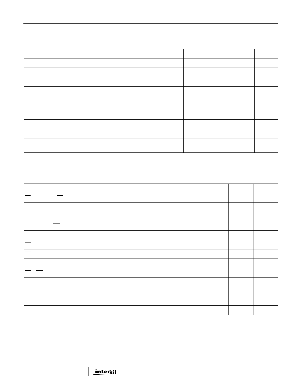
DC Electrical Specifications Test Conditions: V
f
= 2.40MHz, R
CLOCK
Compensated Mode, Unless Otherwise Specified
PARAMETER TEST CONDITIONS MIN TYP MAX UNITS
Input Low Voltage, V
Input High Voltage, V
Output Low Voltage, V
Output High Voltage, V
IL
IH
OL
OH
Three-State Leakage Current,
Pins 18-25, I
Leakage, Pins 15-17, 28, I
Input Capacitance, C
OL
IN
IN
Input Pullup Current (Pins 18-25), I
AC Electrical Specifications T
Pins 15-25, 28 - - 0.8 V
Pins 15-25, 28 2.0 - - V
Pins 16, 18-25, IOL = 1.6mA - - 0.4 V
Pins 16, 18-25, IOH = -400µA 2.4 - - V
All Digital Drivers In High Impedance State,
Parallel Mode. CS = VCC, VIN = 0V, V
VIN = 0V, V
CC
Pins 15, 17-25, 28 - 5 - pF
Pin 16 - 10 - pF
Pins 18-25 at D
PU
SEL = D
= 0oC to 75oC; Test Conditions: VCC = +4.75V, VEE = -5.00V (Note 8), D
A
V
IN LO=AGND
C
= 0.01µF, VIL=0V, VIH = 4V, VOL=VOH = 1.5V, tr = tf < 10ns, 51/2 Digit Compensated Mode,
INT
(Serial Modes)
GND
, V
Unless Otherwise Specified
= +5V,VEE= -5V,D
CC
= 400kΩ, C
INT
GND
= +1.00000V, V
REF HI
=0V,A
GND
= 0.01µF, TA = 25oC, V
INT
CC
REF LO
= A
GND
GND
=0V,V
IN LO
REF HI
= A
= +1.00000V,V
, C
GND
= 1.0µF, 51/2 Digit
REF
REF LO=AGND
--±10 µA
--±1 µA
--5-µA
, f
CLOCK
GND
= 2.40MHz, R
= 0V, A
= 400kΩ,
INT
GND
= 0V,
,
PARAMETER TEST CONDITIONS MIN TYP MAX UNITS
CS Setup/Hold of WR, t
WR Setup of Data In, t
WR Pulse Width, t
Data Hold After WR, t
CS Setup/Hold of RD, t
RD to Data Out, t
RD to Hi-Z State, t
WR to RD, WR to WR, t
RD to WR, t
B
RXD Setup of Data In, t
1
2
3
4
5
6
7
A
C
Data Hold After EXT CLK, t
EXT CLK to DATA OUT, t
CS Setup of TXD, t
f
(Note 7) 25 - - ns
CL = 50pF, VO = 1.5V - - 100 ns
(Note 7) 5/f
(Note 7) 200 - - ns
(Note 7) 60 - - ns
D
E
0--ns
50 - - ns
150 - - ns
20 - - ns
- - 70 ns
CLOCK
40 - - ns
- - 300 ns
100 - - ns
NOTES:
6. All typical values have been characterized but are not production tested.
7. Not production tested, guaranteed by design and characterization.
8. All AC characteristics are guaranteed for VCC = +5V 15%, VEE = -5V 15%, over TA = 0oC to 75oC.
--s
3

Timing Waveforms
CS
t
WR
P0 - P7
1
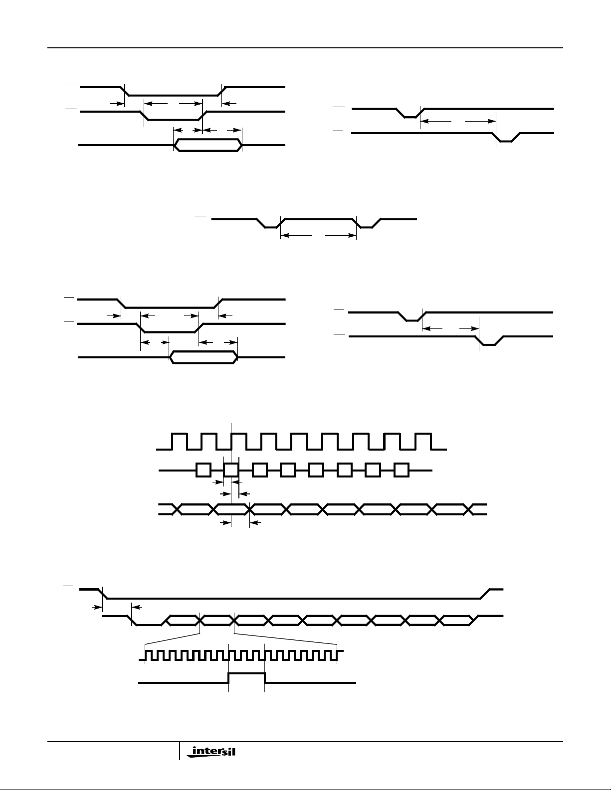
FIGURE 1A. WRITE FIGURE 1B. WRITE TO READ CYCLE
CS
t
RD
P0 - P7 DATA OUT
5
t
3
t
2
DATA IN
WR
t
t
6
HI-7159A
t
1
t
4
t
A
FIGURE 1C. WRITE TO WRITE CYCLE
5
t
7
WR
RD
RD
WR
t
A
t
B
CS
TXD OR RXD
DATA CLOCK
BIT DETECTOR
SAMPLE TIME
FIGURE 1D. READ FIGURE 1E. READ TO WRITE CYCLE
FIGURE 1. PARALLEL MODE TIMING
CLK
(PIN 15)
RXD/TXD
(PIN 16)
RXD/TXD
(PIN 16)
D0
D1 D2 D3 D4 D5
t
C
t
D
D0 D1 D2 D3 D4 D5 D6 D7
t
E
D6 D7
(HI-7159A RECEIVING)
(HI-7159A TRANSMITTING)
FIGURE 2A. SERIAL MODE 0 TIMING
t
f
START
0123
D0 D1 D2 D3 D4 D5 D6 D7
456789
10 11
12 13 14
15
PARITY STOP
(SERIAL MODE 1)
NOTE: All input timing shown is defined at 50% points.
4
FIGURE 2B. SERIAL MODE TIMING

HI-7159A
Pin Descriptions
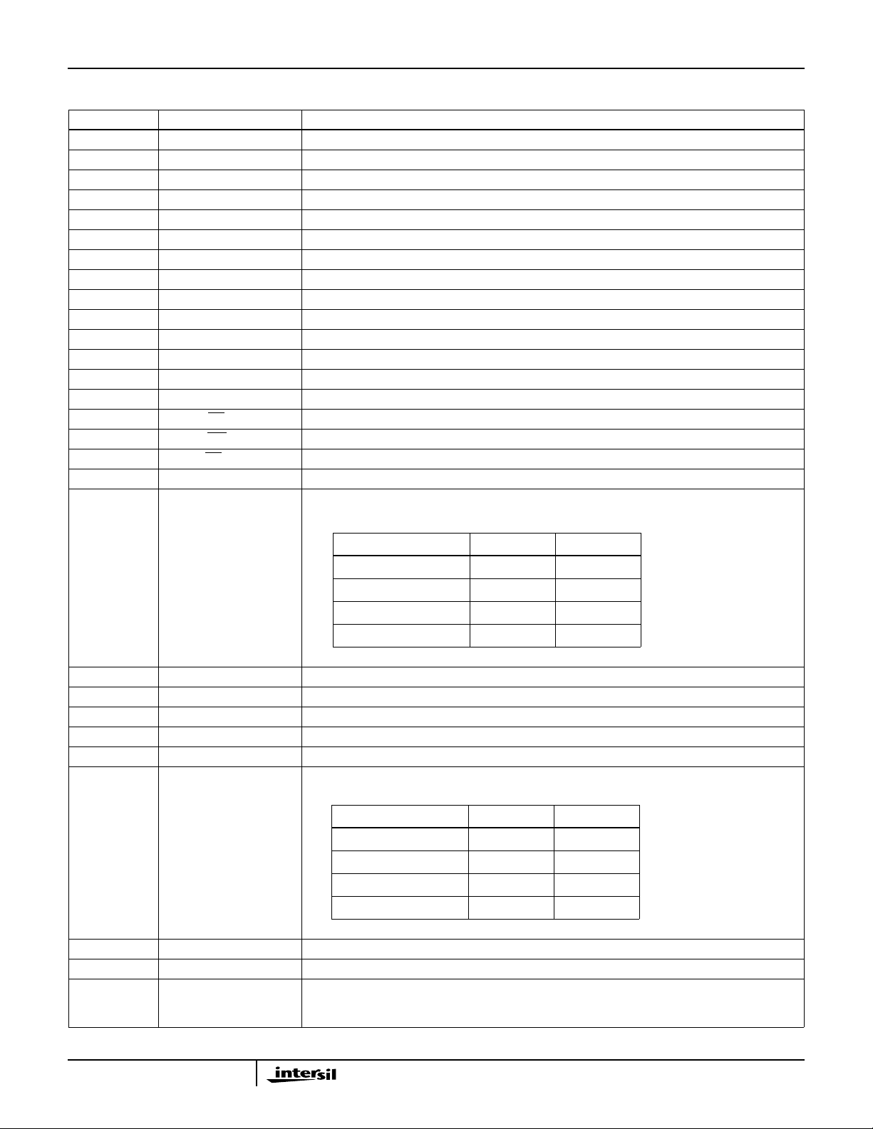
PIN SYMBOL DESCRIPTION
1VCCPositive 5V Power Supply for analog and digital sections.
2 INT OUT Integrator Output; external component terminal.
3 INT IN Integrator Input; external component terminal.
4 BUF OUT V
5C
6C
7C
8C
9V
10 V
11 A
12 V
13 V
14 V
- Guard Reference Capacitor guard ring terminal (negative).
REF
- Reference Capacitor negative terminal.
REF
+ Reference Capacitor positive terminal.
REF
+ Guard Reference Capacitor guard ring terminal (positive).
REF
REF HI
REF LO
GND
IN HI
IN LO
EE
15 RD/RXD Parallel Read; serial receive (modes 1 and 2), serial clock (mode 0).
16 WR/TXD Parallel Write; serial transmit (modes 1 and 2), serial receive/transmit (mode 0).
17 CS/SAD4 Chip Select (parallel and serial modes 0 and 1), serial address bit 4 (mode 2).
18 P0/SMS0 Parallel I/O Port (P0); serial mode select pin.
19 P1/SMS1 Parallel I/O Port (P1); serial mode select pin.
Voltage Buffer Output; external component terminal.
IN HI
Positive Reference Input terminal.
Negative Reference Input terminal.
Analog Ground (0V).
Positive Analog Input Voltage terminal.
Negative Analog Input Voltage terminal.
Negative 5V Power Supply for analog section.
MODE SMS0 SMS1
Serial Mode 0 0 0
Serial Mode 1 0 1
Serial Mode 2 1 0
Reserved 1 1
20 P2/SAD0 Parallel I/O Port (P2); serial address bit 0.
21 P3/SAD1 Parallel I/O Port (P3); serial address bit 1.
22 P4/SAD2 Parallel I/O Port (P4); serial address bit 2.
23 P5/SAD3 Parallel I/O Port (P5); serial address bit 3.
24 P6/BRS0 Parallel I/O Port (P6); serial baud rate select.
25 P7/BRS1 Parallel I/O Port (P7); serial baud rate select.
BAUD RATE BRS0 BRS1
300 0 0
1200 0 1
9600 1 0
19200 1 1
26 D
27 X
GND
TAL
Digital Ground (0V).
Oscillator Out; crystal connection pin (other crystal pin connected to VCC).
28 SEL Select pin for parallel or serial operation.
Parallel SEL = 1
Serial Modes SEL = 0
5
