

Intersil Corporation HI7133 Datasheet
August 1997
HI7131, HI7133
31/2 Digit, Low Power, High CMRR,
LCD/LED Display-Type A/D Converters
Features
• 120dB CMRR Equal to ±0.01 Count/V of Common
Mode Voltage Error
• Fast Recovery from Input Overrange Results “Correct
First-Reading” After Overload
• Guaranteed 0000 Reading for 0V Input
• True Polarity at Zero for Precise Null Detection
• 1pA Input Current (Typ)
• True Differential Input and Reference
• Single or Dual Supply Operation Capability
• Direct LCD Display Drive - HI7131
• Direct LED Display Drive - HI7133
• Low Noise, 15µV
Hangover
• Low Power Dissipation, Guaranteed Less Than 1mW,
Results 8000 Hours (Typ) 9V Battery Life
• No Additional Active Components Required
Without Hysteresis or Overrange
P-P
Applications
• Handheld Instruments
• Basic Measurements: Voltage, Current, Resistance
Pressure, Temperature, Fluid Flow and Level, pH,
Weight, Light Intensity
• DMMs and DPMs
Description
The Intersil HI7131 and HI7133 are 31/2 digit, A/D converters that have been optimized for superior DC Common
Mode Rejection (CMRR) when used with a split ±5V supply
or a single 9V battery. The HI7131 contains all the necessary active components on a single IC to directly interface an
LCD (Liquid Crystal Display). The supply current is under
100µA and is ideally suited for battery operation. The HI7133
contains all the necessary active components on a single IC
to directly interface an LED (Light Emitting Diode).
The HI7131 and HI7133 feature high accuracy performance
like, 120dB of CMRR, auto-zero to less than 10µV of offset,
fast recovery from over load, zero drift of less than 1µV/
input bias current of 10pA maximum, and rollover error of
less than one count. A true differential signal and reference
inputs are useful features in all systems, but gives the
designer an advantage when measuring load cells, strain
gauges and other bridge-type transducers.
The HI7131 and HI7133 are supplied in a 40 lead plastic DIP
and a 44 lead metric plastic quad flatpack package.
o
C,
Ordering Information
TEMP.
PART NO.
HI7131CPL 0 to 70 40 Ld PDIP E40.6
HI7131CM44 0 to 70 44 Ld MQFP Q44.10x10
HI7133CPL 0 to 70 40 Ld PDIP E40.6
HI7133CM44 0 to 70 44 Ld MQFP Q44.10x10
RANGE (oC) PACKAGE PKG. NO.
CAUTION: These devices are sensitive to electrostatic discharge; follow proper IC Handling Procedures.
http://www.intersil.com or 407-727-9207
| Copyright © Intersil Corporation 1999
3-1826
File Number 3373.2
Pinouts
HI7131, HI7133
V+
D1
C1
B1
(UNITS)
(TENS)
(100’S)
(1000) AB4
(MINUS) POL
A1
F1
G1
E1
D2
C2
B2
A2
F2
E2
D3
B3
F3
E3
HI7131CPL, HI7133CPL
(PDIP)
TOP VIEW
1
2
3
4
5
6
7
8
9
10
11
12
13
14
15
16
17
18
19
20
OSC 1
40
OSC 2
39
OSC 3
38
TEST
37
REF HI
36
REF LO
35
C
34
REF
C
33
REF
32
COMMON
31
IN HI
30
IN LO
29
A-Z
28
BUFF
27
INT
V-
26
25
G2 (TENS)
24
C3
23
A3
22
G3
21
BP/GND
+
-
(100’S)
NC
NC
TEST
OSC3
NC
OSC2
OSC1
V+
D1
C1
B1
HI7131CM44, HI7133CM44
(MQFP)
TOP VIEW
REF HI
REF LO
CREF+
CREF-
COMMON
44 43 42 41 40
1
2
3
4
5
6
7
8
9
10
11
12 13 14 15 16 17
F1
A1
G1
39 38 37 36 35 34
B1D2C2B2A2F2B2
IN HI
IN LO
A-Z
BUFF
INT
2221201918
V-
33
32
31
30
29
28
27
26
25
24
23
D3
NC
G2
C3
A3
G3
BPGND
POL
AB4
E3
F3
B3
3-1827
HI7131, HI7133
LCD/LED
DISPLAY
ANALOG
INPUT
EXTERNAL
CLOCK
EXTERNAL
REFERENCE
R
IN
EXTERNAL
INPUT
Critical Components General Specifications:
1. C
: Low dielectric absorption capacitor,
INT
polypropylene or similar
2. CAZ, C
, CIN: Low leakage capacitors
REF
A-Z
BUFF
INT
IN HI
IN LO
COMMON
V+
OSC1
OSC2
OSC3
C
REF
C
REF
REF HI
REF LO
+
-
V-
FIGURE 89. TYPICAL APPLICATION CIRCUIT
HI7131, HI7133
DUT
C
1M
VREF
C
C
R
C
IN
AZ
INT
INT
1µF
C
REF
0.01µF
0.1µF
0.47µF
180K
0.047µF
40
39
38
37
36
35
34
33
32
31
30
29
28
27
OSC 1
OSC 2
OSC 3
TEST
REF HI
REF LO
+
C
REF
C
-
REF
COMMON
IN HI
IN LO
A-Z
BUFF
INT
V+
D1
C1
B1
A1
F1
G1
E1
D2
C2
B2
A2
F2
E2
D3
B3
F3
E3
AB4
POL
BP/GND
G3
A3
C3
G2
V-
FIGURE 90. TEST CIRCUIT
9V
+5V
0.47µF
1
1
2
3
4
5
6
7
8
9
10
11
12
13
14
15
16
17
18
19
20
21
22
23
24
25
26
0.47µF
-5V
LCD/LED
DISPLA Y
AND
TEST
LOGIC
= 0.01µF
C
IN
C
REF
C
INT
= 0.1µF
= 0.047µF
C
C
AZ
VRH
R
R
= 0.47µF
= 1MΩ
IN
= 180kΩ
INT
=1µF
3-1828
HI7131, HI7133
Absolute Maximum Ratings Thermal Information
Supply Voltage, V+ to V-. . . . . . . . . . . . . . . . . . . . . . . . . . . . . . +15V
Signal Inputs, Pin# 30, 31 (Note 1). . . . . . . . . . . . . . . . . . . . V+ to V-
Reference Inputs, Pin# 35, 36 . . . . . . . . . . . . . . . . . . . . . . . V+ to V-
Clock Input, OSC1, Pin# 40 (Note 2) . . . . . . . . . . . . TEST pin to V+
All Other Analog Leads, Pin# 27-29, 32-34 . . . . . . . . . . . . . V+ to V-
All Other Digital Leads,
Pin# 2-25, 38, 39 (Note 2). . . . . . . . . . . . . . . . . . . TEST Pin to V
Thermal Resistance (Typical, Note 3) θJA (oC/W)
PDIP Package. . . . . . . . . . . . . . . . . . . . . . . . . . . . . 50
MQFP Package. . . . . . . . . . . . . . . . . . . . . . . . . . . . 80
Maximum Junction Temperature. . . . . . . . . . . . . . . . . . . . . . . 150oC
Maximum Storage Temperature Range . . . . . . . . . .-65oC to 150oC
Maximum Lead Temperature, PDIP Package (Soldering 10s) 300oC
+
(MQFP - Lead Tips Only)
Operating Conditions
Operating Temperature, TA. . . . . . . . . . . . . . . . . . . . . . .0oC to 70oC
CAUTION: Stresses above those listed in “Absolute Maximum Ratings” may cause permanent damage to the device. This is a stress only rating and operation
of the device at these or any other conditions above those indicated in the operational sections of this specification is not implied.
NOTES:
1. Input voltages may exceed the supply voltages provided the input current is limited to ±100µA.
2. TEST pin is connected to internally generated digital ground through a 500Ω resistor (see text for TEST pin description).
3. θJA is measured with the component mounted on an evaluation PC board in free air.
Electrical Specifications (Notes 5, 6, 7) T
Full Scale Range (FSR) = 200.0mV, Unless Otherwise Specified
PARAMETER TEST CONDITIONS MIN TYP MAX UNITS
ACCURACY
Zero Input Reading VIN = 0V -000 ±000 +000 Reading
Ratiometric Reading V
Rollover Error VIN = ±199mV - ±0.2 ±1 Count
IN HI
V
REF HI
= 25oC. Device is Tested in the Circuit Shown in Figure 2.
A
= V
REF HI
- V
, V
REF LO
= V
IN LO
= 100mV
REF LO
= V
COMMON
999 999/
1001 Reading
1000
Linearity Error FSR = 200mV or 2V (Notes 5, 8) - ±0.2 ±1 Count
Zero Input Reading Drift VIN = 0V
Over Full Temperature Range
- ±0.2 ±1
±0.01
µV/oC
Count/oC
(Notes 5, 8)
Scale Factor Temperature Coefficient VIN = 199mV, Over Full Temperature Range,
Reference Drift Not Included (Notes 5, 8)
Equivalent Input Noise (Peak-To-Peak
VIN = 0V (Notes 5, 8) - 15
Value Not Exceeded 95% of the Time)
- ±1 ±5
±0.01
0.15
ppm/oC
Count/oC
- µV
Count
INPUT
Common Mode Voltage Sensitivity VCM = ±1V, VIN = 0V (Notes 5, 6, 8, 9) - - 1
0.01
µV/V
Count/V
Input Leakage Current VIN = 0V (Notes 5, 8) - 1 10 pA
Overload Recovery Period VIN Changing from ±10V to 0V
(Notes 5, 8)
- - 1 Conversion
Cycle
COMMON PIN
COMMON Pin Voltage (With Respect
to V+, i.e., V+ - V
COMMON
)
COMMON Pin Voltage Temperature
V+ to V- = 10V 2.4 2.8 3.2 V
V+ to V- = 10V (Notes 5, 8) - 150 - ppm/oC
Coefficient
COMMON Pin Sink Current +0.1V Change on V
COMMON Pin Source Current -0.1V Change on V
COMMON
COMMON
(Note 5) - 3 - mA
(Note 5) - 1 - µA
3-1829
HI7131, HI7133
Electrical Specifications (Notes 5, 6, 7) T
Full Scale Range (FSR) = 200.0mV, Unless Otherwise Specified (Continued)
PARAMETER TEST CONDITIONS MIN TYP MAX UNITS
DISPLAY DRIVER (HI7131)
Peak-To-Peak Segment Drive Voltage V+ to V- = 10V 4 5 6 V
Peak-To-Peak Backplane Drive Volt-
age
POWER SUPPLY (Nominal Supply Voltage; V+ to V- = 10V)
Supply Current (Does Not Include
COMMON Pin Current)
Power Dissipation Capacitance VS Clock Frequency (Notes 5, 8) - 40 - pF
DISPLAY DRIVER (HI7133)
Segment Sink Current
(Except Pins 19 and 20)
Pin 19 Sink Current 10 16 - mA
Pin 20 Sink Current 47- mA
POWER SUPPLY Nominal Supply Voltage; V+ = +5V, V- = -5V, Both Respect to GND Pin
V+ Supply Current (Note 10) VIN = 0V
V- Supply Current (Notes 5, 10) - 40 - µA
VIN = 0V (Note 10)
Oscillator Frequency = 16kHz
V+ = +5.0V
Driver Pin Voltage = 3.0V
Oscillator Frequency = 16kHz
Does Not Include COMMON Pin and Display
Current
= 25oC. Device is Tested in the Circuit Shown in Figure 2.
A
456 V
- 70 100 µA
5 8.5 - mA
- 70 100 µA
Power Dissipation Capacitance Versus Clock Frequency (Notes 5, 8) - 40 - pF
NOTES:
4. Dissipation rating assumes device is mounted with all leads soldered to printed circuit board.
5. All typical values have been characterized but not tested.
6. See “Parameters Definition” section.
7. Count is equal to one number change in the least significant digit of the display.
8. Parameter not tested on a production basis, guaranteed by design and/or characterization.
9. See “Differential Input” section.
10. 48kHz oscillator increases current by 20µA (Typ).
3-1830
HI7131, HI7133
Design Information Summary Sheet
• OSCILLATOR FREQUENCY
≈ 0.45/RC
f
OSC
C
≥ 50pF
OSC
R
> 50kΩ
OSC
C
= 50pF, R
OSC
• CLOCK FREQUENCY
CLOCK
= f
f
• CLOCK PERIOD
CLOCK
= 1/f
t
• CONVERSION CYCLE
= 4000 x t
T
CYC
For f
OSC
• SIGNAL INTEGRATION PERIOD
= 1000 x t
T
INT
• 60/50Hz REJECTION CRITERIA
/ t
T
INT
60Hz
• OPTIMUM FULL SCALE ANALOG INPUT RANGE
= 200mV to 2V
V
INFS
• INPUTS VOLTAGE RANGE
(V- + 1V) < V
• MAXIMUM INTEGRATION CURRENT
I
INT(MAX)
Maximum integration current should be the maximum
buffer output current with no nonlinearity effect.
Maximum Buffer Output Current = 1µA
• INTEGRATOR MAXIMUM OUTPUT VOLTAGE SWING
V
INT(MAX)
(V- + 0.5) < V
(Typ) V
INT(MAX)
(OSC)
OSC
/4
OSC
CLOCK
CLOCK
= 40kHz; T
CLOCK
or T
INT
or V
IN LO
= V
= (T
/ R
INFS
) (I
INT
INT(MAX)
= 2V
= 180kΩ; f
= 16000 x t
= 400ms
CYC
/ t
= Integer
50Hz
< (V+ - 1V)
IN HI
INT
INT(MAX)
< (V+ - 0.5)
)/C
OSC
OSC
INT
(Typ) = 48kHz
• INTEGRATING RESISTOR
= V
R
INT
INFS
/ I
INT(MAX)
• INTEGRATING CAPACITOR
= (T
C
INT
INT
) (I
INT(MAX)
) / V
INT(MAX)
• AUTO-ZERO CAPACITOR VALUE
REFERENCE CAPACITOR VALUE
0.1µF < C
REF
< 1µF
• REFERENCE INPUTS VOLTAGE RANGE
V- < V
REFLO
or V
REFHI
< V+
• REFERENCE VOLTAGE
V
REF
= V
INFS
/2
• COMMON PIN VOLTAGE
V
COMMON
= V+ - 2.8, (Typ), V
COMMON
is regulated and
can be used as a reference. It is biased between V+ and
V- and regulation is lost at (V+ -V-) < 6.8V. V
COMMON
does not have sink capability and can be externally pulled
down to lower voltages.
• DISPLAY TYPE
LCD, Non-Multiplexed
• POWER SUPPLY, V+ TO V-
Single +9V or 5V Nominal, +5V to +12V Functional
• DISPLAY READING
/ V
Reading = 1000 x (V
IN
Maximum Reading = 1999, for V
REF
)
= 1.999 x V
IN
REF
pin
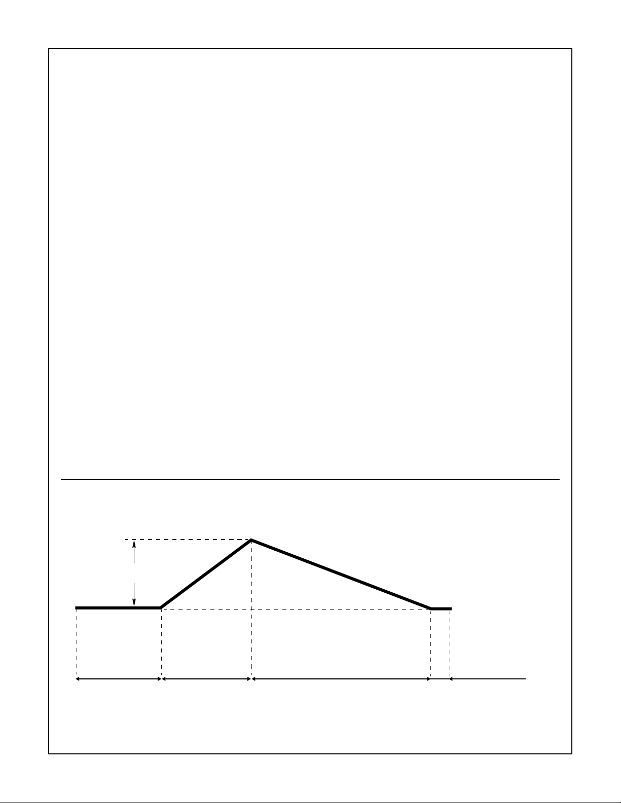
Typical Integrator Amplifier Output Waveform (INT Pin)
INTEGRATOR
VOLTAGE SWING
AUTO-ZERO PHASE
100 COUNTS OR
990 - 2990 COUNTS
NOTE: 1 Count = 1 Clock Cycle = 4 Oscillator Cycles.
SIGNAL INTEGRATE
PHASE FIXED
1000 COUNTS
4000 COUNTS: TOTAL OF EACH CONVERSION CYCLE
DEINTEGRATE PHASE
0 - 2000 COUNTS
3-1831
ZERO INTEGRATE PHASE
10 COUNTS OR
900 COUNTS

HI7131, HI7133
Pin Descriptions
PIN NUMBER
44 PIN
FLATPACK
1 8 V+ Supply Power Supply.
2 9 D1 Output Driver Pin for Segment “D” of the display units digit.
3 10 C1 Output Driver Pin for Segment “C” of the display units digit.
4 11 B1 Output Driver Pin for Segment “B” of the display units digit.
5 12 A1 Output Driver Pin for Segment “A” of the display units digit.
6 13 F1 Output Driver Pin for Segment “F” of the display units digit.
7 14 G1 Output Driver Pin for Segment “G” of the display units digit.
8 15 E1 Output Driver Pin for Segment “E” of the display units digit.
9 16 D2 Output Driver Pin for Segment “D” of the display tens digit.
10 17 C2 Output Driver Pin for Segment “C” of the display tens digit.
11 18 B2 Output Driver Pin for Segment “B” of the display tens digit.
12 19 A2 Output Driver Pin for Segment “A” of the display tens digit.
13 20 F2 Output Driver Pin for Segment “F” of the display tens digit.
14 21 E2 Output Driver Pin for Segment “E” of the display tens digit.
15 22 D3 Output Driver pin for segment “D” of the display hundreds digit.
16 23 B3 Output Driver pin for segment “B” of the display hundreds digit.
17 24 F3 Output Driver pin for segment “F” of the display hundreds digit.
18 25 E3 Output Driver pin for segment “E” of the display hundreds digit.
19 26 AB4 Output Driver pin for both “A” and “B” segments of the display thousands digit.
20 27 POL Output Driver pin for the negative sign of the display.
21 28 BP/GND Output Driver pin for the LCD backplane/Power Supply Ground.
22 29 G3 Output Driver pin for segment “G” of the display hundreds digit.
23 30 A3 Output Driver pin for segment “A” of the display hundreds digit.
24 31 C3 Output Driver pin for segment “C” of the display hundreds digit.
25 32 G2 Output Driver pin for segment “G” of the display tens digit.
26 34 V- Supply Negative power supply.
27 35 INT Output Integrator amplifier output. To be connected to integrating capacitor.
28 36 BUFF Output Input buffer amplifier output. To be connected to integrating resistor.
29 37 A-Z Input Integrator amplifier input. To be connected to auto-zero capacitor.
30
31
32 40 COMMON Supply/
33
34
35
36
37 3 TEST Input Display test. Turns on all segments when tied to V+.
38
39
40
38
39
41
42
43
44
4
6
7
NAME FUNCTION DESCRIPTION40 PIN DIP
IN LO
IN HI
C
REF
C
REF
REF LO
REF HI
OSC3
OSC2
OSC1
Input Differential inputs. To be connected to input voltage to be measured. LO and HI
designators are for reference and do not imply that LO should be connected to
lower potential, e.g., for negative inputs IN LO has a higher potential than IN HI.
Internal voltage reference output.
Output
-
+
Input Input pins for reference voltage to the device. REF HI should be positive
Output
Output
Input
Connection pins for reference capacitor.
reference to REF LO.
Device clock generator circuit connection pins.
3-1832
 Loading...