Intersil Corporation HI-774, HI-674A, HI-574A Datasheet
August 1997
HI-574A, HI-674A,
HI-774
Complete, 12-Bit A/D Converters
with Microprocessor Interface
Features
• Complete 12-Bit A/D Converter with Reference and Clock
• Full 8-Bit, 12-Bit or 16-Bit Microprocessor Bus Interface
• Bus Access Time. . . . . . . . . . . . . . . . . . . . . . . . . .150ns
• No Missing Codes Over Temperature
• Minimal Setup Time for Control Signals
• Fast Conversion Times
- HI-574A (Max) . . . . . . . . . . . . . . . . . . . . . . . . . . . . 25µs
- HI-674A (Max) . . . . . . . . . . . . . . . . . . . . . . . . . . . . 15µs
- HI-774 (Max) . . . . . . . . . . . . . . . . . . . . . . . . . . . . . . 9µs
• Digital Error Correction (HI-774)
• Low Noise, via Current-Mode Signal
Transmission Between Chips
• Byte Enable/Short Cycle (A
Input)
O
- Guaranteed Break-Before-Make Action, Eliminating
Bus Contention During Read Operation. Latched by
Start Convert Input (T o Set the Conversion Length)
• Supply Voltage. . . . . . . . . . . . . . . . . . . . . ±12V to ±15V
Applications
• Military and Industrial Data Acquisition Systems
• Electronic Test and Scientific Instrumentation
• Process Control Systems
Description
The HI-X74(A) is a complete 12-bit, Analog-to-Digital
Converter, including a +10V reference clock, three-state outputs and a digital interface for microprocessor control. Successive approximation conversion is performed by two monolithic
dice housed in a 28 lead package. The bipolar analog die features the Intersil Dielectric Isolation process, which provides
enhanced AC performance and freedom from latch-up.
Custom design of each IC (bipolar analog and CMOS digital)
has yielded improved performance over existing versions of
this converter. The voltage comparator features high PSRR
plus a high speed current-mode latch, and provides precise
decisions down to 0.1 LSB of input overdrive. More than 2X
reduction in noise has been achieved by using current
instead of voltage for transmission of all signals between the
analog and digital ICs. Also, the clock oscillator is current
controlled for excellent stability over temperature.
The HI-X74(A) offers standard unipolar and bipolar input
ranges, laser trimmed for specified linearity, gain and offset
accuracy. The low noise buried zener reference circuit is
trimmed for minimum temperature coefficient.
Power requirements are +5V and ±12V to ±15V, with typical
dissipation of 385mW (HI-574A/674A) and 390mW (HI-774) at
12V. All models are available in sidebrazed DIP, PDIP, and
CLCC. For additional HI-Rel screening including 160 hour b urnin, specify “-8” suffix. For MIL-STD-883 compliant parts, request
HI-574A/883, HI-674A/883, and HI-774/883 data sheets.
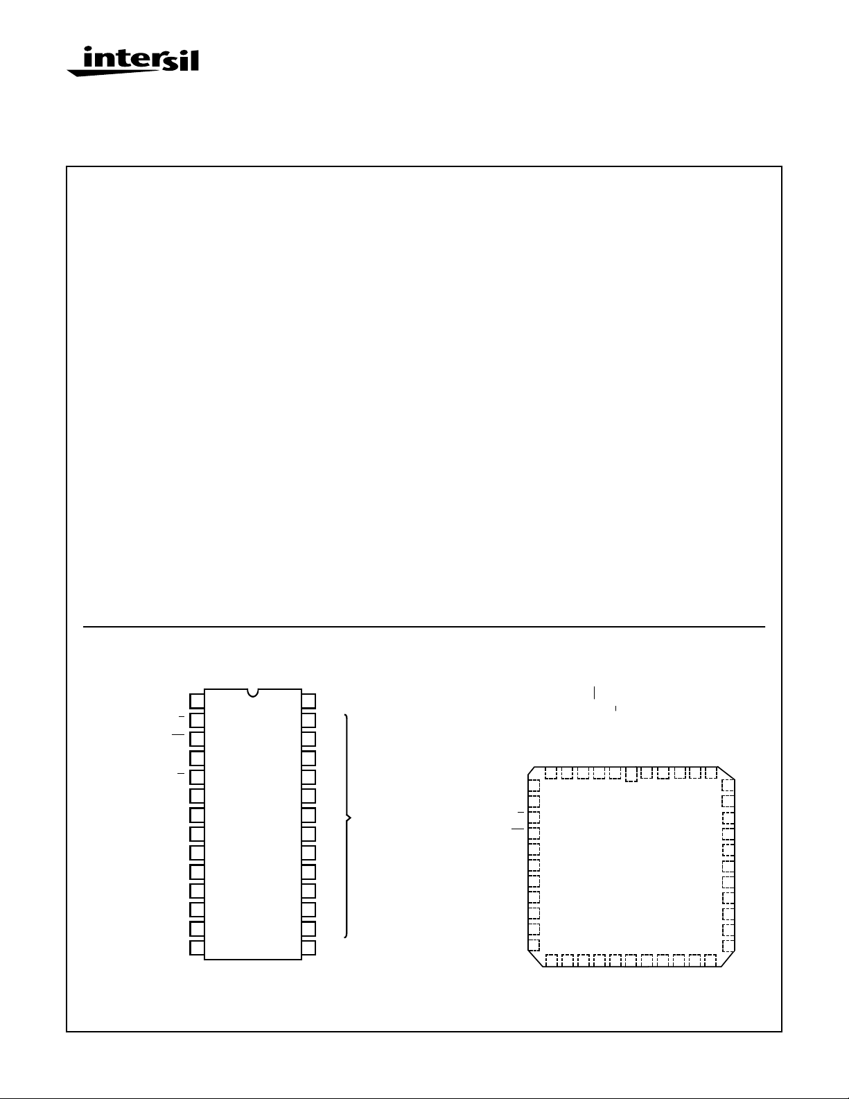
Pinouts
(PDIP, SBDIP)
TOP VIEW
+5V SUPPL Y, V
DATA MODE SEL, 12/
CHIP SEL, CS
BYTE ADDR/SHORT
CYCLE, A
READ/CONVERT , R/
CHIP ENABLE, CE
+12V/+15V SUPPL Y, V
+10V REF , REF OUT
ANALOG
COMMON, AC
REFERENCE INPUT
-12V/-15V SUPPLY , V
BIPOLAR OFFSET
BIP OFF
10V INPUT
20V INPUT
CAUTION: These devices are sensitive to electrostatic discharge; follow proper IC Handling Procedures.
1-888-INTERSIL or 321-724-7143 | Copyright © Intersil Corporation 1999
LOGIC
CC
EE
1
2
8
3
4
O
5
C
6
7
8
9
10
11
12
13
14
28
STATUS, STS
27
DB11
26
DB10
25
DB9
24
DB8
23
DB7
22
DB6
21
DB5
20
DB4
19
DB3
18
DB2
17
DB1
16
DB0
DIG COMMON,
15
DC
MSB
DIGITAL
DATA
OUTPUTS
LSB
READ CONVERT, R/C
CHIP ENABLE, CE
+15V SUPPLY, V
+10V REFERENCE,
ANALOG COMMON, AC
REFERENCE INPUT,
REF OUT
-15V SUPPLY, V
BIPOLAR OFFSET,
6-952
REF IN
BIP OFF
NC
NC
CC
EE
NC
6 3
7
8
9
10
11
12
13
14
15
16
17
(CLCC)
TOP VIEW
BYTE ADDRESS/
NC
NC
4
NCNCNC
10V
20V
O
CS
SHORT CYCLE, A
CHIP SELECT,
SELECT, 12/8
DATA MODE
25
LOGIC
+5V SUPPLY, V
STATUS, STS
DB11, MSB
DB10
NC
NC
(LSB) DB0
NC
40414243
39
38
37
36
35
34
33
32
31
30
29
2827262524232221201918
DB1
1
NC
44
DC
DIG
COMMON,
NC
File Number 3096.4
NC
NC
DB9
DB8
DB7
DB6
DB5
DB4
DB3
NC
DB2
HI-574A, HI-674A, HI-774
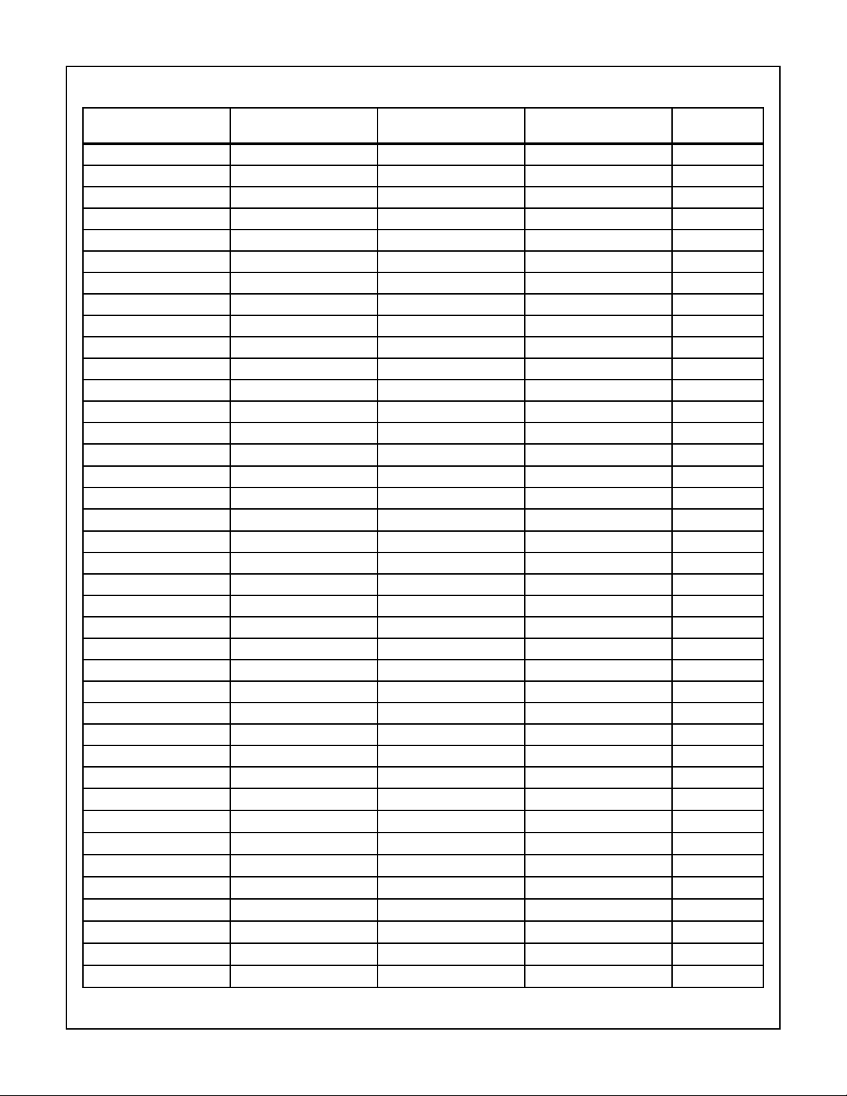
Ordering Information
TEMPERA TURE RANGE
PART NUMBER INL
HI3-574AJN-5 ±1.0 LSB 0 to 75 28 Ld PDIP E28.6
HI3-574AKN-5 ±0.5 LSB 0 to 75 28 Ld PDIP E28.6
HI3-574ALN-5 ±0.5 LSB 0 to 70 28 Ld PDIP E28.6
HI1-574AJD-5 ±1.0 LSB 0 to 75 28 Ld SBDIP D28.6
HI1-574AKD-5 ±0.5 LSB 0 to 75 28 Ld SBDIP D28.6
HI1-574ALD-5 ±0.5 LSB 0 to 75 28 Ld SBDIP D28.6
HI1-574ASD-2 ±1.0 LSB -55 to 125 28 Ld SBDIP D28.6
HI1-574ATD-2 ±0.5 LSB -55 to 125 28 Ld SBDIP D28.6
HI1-574AUD-2 ±0.5 LSB -55 to 125 28 Ld SBDIP D28.6
HI1-574ASD/883 ±1.0 LSB -55 to 125 28 Ld SBDIP D28.6
HI1-574ATD/883 ±0.5 LSB -55 to 125 28 Ld SBDIP D28.6
HI1-574AUD/883 ±0.5 LSB -55 to 125 28 Ld SBDIP D28.6
HI4-574ASE/883 ±1.0 LSB -55 to 125 44 Ld CLCC J44.A
HI4-574ATE/883 ±0.5 LSB -55 to 125 44 Ld CLCC J44.A
HI4-574AUE/883
HI3-674AJN-5 ±1.0 LSB 0 to 75 28 Ld PDIP E28.6
HI3-674AKN-5 ±0.5 LSB 0 to 75 28 Ld PDIP E28.6
HI3-674ALN-5
HI1-674AJD-5 ±1.0 LSB 0 to 75 28 Ld SBDIP D28.6
HI1-674AKD-5 ±0.5 LSB 0 to 75 28 Ld SBDIP D28.6
HI1-674ALD-5 ±0.5 LSB 0 to 75 28 Ld SBDIP D28.6
HI1-674ASD-2 ±1.0 LSB -55 to 125 28 Ld SBDIP D28.6
HI1-674ATD-2 ±0.5 LSB -55 to 125 28 Ld SBDIP D28.6
HI1-674AUD-2 ±0.5 LSB -55 to 125 28 Ld SBDIP D28.6
HI1-674ASD/883 ±1.0 LSB -55 to 125 28 Ld SBDIP D28.6
HI1-674ATD/883 ±0.5 LSB -55 to 125 28 Ld SBDIP D28.6
HI1-674AUD/883 ±0.5 LSB -55 to 125 28 Ld SBDIP D28.6
HI4-674ASE/883 ±1.0 LSB -55 to 125 44 Ld CLCC J44.A
HI4-674ATE/883 ±0.5 LSB -55 to 125 44 Ld CLCC J44.A
HI4-674AUE/883 ±0.5 LSB -55 to 125 44 Ld CLCC J44.A
HI3-774J-5
HI3-774K-5
HI1-774J-5
HI1-774K-5
HI1-774U-2
HI1-774T/883
HI4-774S/883
HI4-774T/883
HI4-774U/883
±0.5 LSB
±0.5 LSB
±1.0 LSB 0 to 75 28 Ld PDIP E28.6
±0.5 LSB 0 to 75 28 Ld PDIP E28.6
±1.0 LSB 0 to 75 28 LdSBDIP
±0.5 LSB 0 to 75 28 LdSBDIP
±0.5 LSB -55 to 125 28 Ld SBDIP
±0.5 LSB -55 to 125 28 Ld SBDIP
±1.0 LSB -55 to 125 44 Ld CLCC
±0.5 LSB -55 to 125 44 Ld CLCC
±0.5 LSB -55 to 125 44 Ld CLCC
(oC) PACKA GE PKG. NO.
-55 to 125 44 Ld CLCC J44.A
0 to 75 28 Ld PDIP E28.6
D28.6
D28.6
D28.6
D28.6
J44.A
J44.A
J44.A
6-953
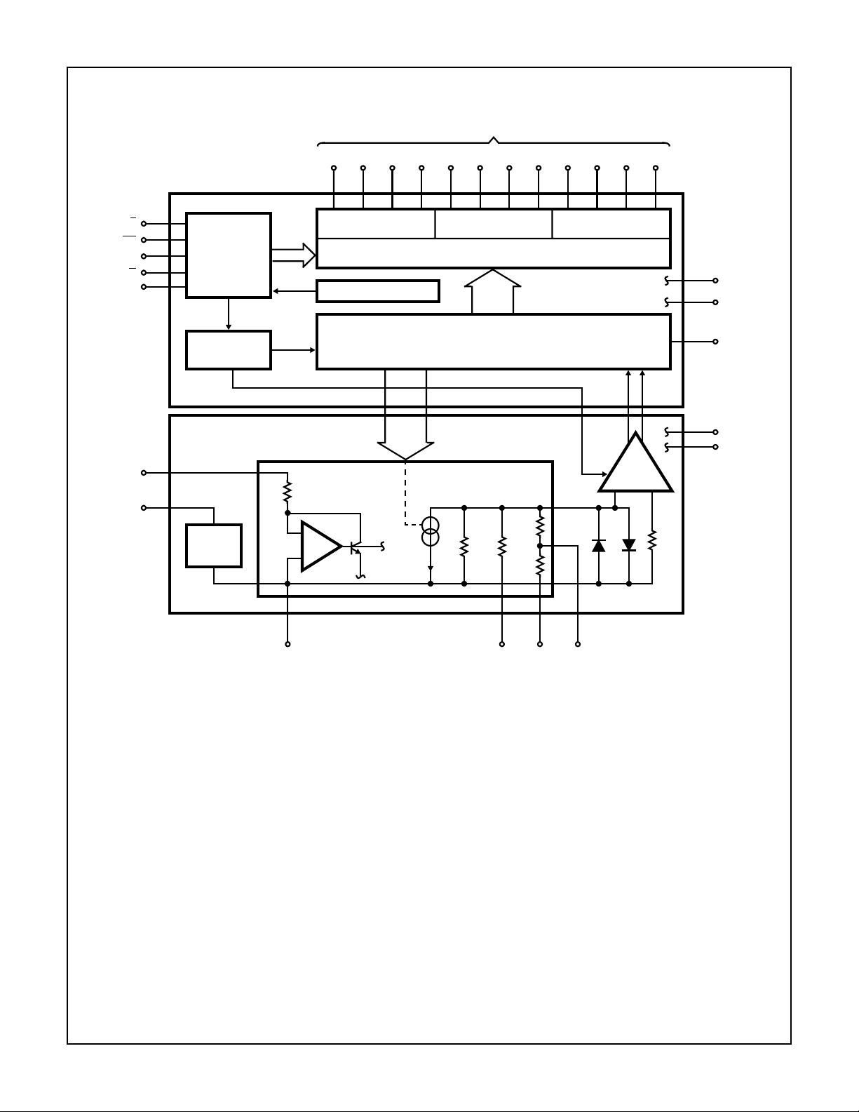
Functional Block Diagram
HI-574A, HI-674A, HI-774
BIT OUTPUTS
MSB LSB
12/8
CS
A
O
R/C
CE
IN
V
REF
V
OUT
REF
CONTROL
LOGIC
OSCILLATOR
DIGITAL CHIP
ANALOG CHIP
+10V
REF
THREE-STATE BUFFERS AND CONTROL
POWER-UP RESET
CLK
12 BITS
10K
+
-
5K
NIBBLE B (NOTE) NIBBLE C (NOTE)NIBBLE A (NOTE)
12 BITS
SAR
DAC
10K
STROBE
5K
5K
-
COMP
+
2.5K
V
LOGIC
DIGITAL
COMMON
STS
V
CC
V
EE
ANALOG
COMMON
NOTE: “Nibble” is a 4-bit digital word.
BIP
OFF
20V
INPUT
10V
INPUT
6-954
HI-574A, HI-674A, HI-774
Absolute Maximum Ratings Thermal Information
Supply Voltage
VCC to Digital Common . . . . . . . . . . . . . . . . . . . . . . 0V to +16.5V
VEE to Digital Common. . . . . . . . . . . . . . . . . . . . . . . 0V to -16.5V
V
to Digital Common. . . . . . . . . . . . . . . . . . . . . . 0V to +7V
LOGIC
Analog Common to Digital Common±1V
Control Inputs
(CE, CS, AO, 12/8, R/C) to Digital Common . . -0.5V to V
Analog Inputs
(REFIN, BIPOFF, 10VIN) to Analog Common. . . . . . . . . . ±16.5V
20VIN to Analog Common . . . . . . . . . . . . . . . . . . . . . . . . . . ±24V
REFOUT . . . . Indefinite Short To Common, Momentary Short To V
LOGIC
+0.5V
Operating Conditions
Temperature Range
HI3-574AxN-5, HI1-574AxD-5 . . . . . . . . . . . . . . . . . .0oC to 75oC
HI3-674AxN-5, HI1-674AxD-5 . . . . . . . . . . . . . . . . . .0oC to 75oC
HI3-774xN-5, HI1-774xD-5. . . . . . . . . . . . . . . . . . . . .0oC to 75oC
HI1-574AxD-2, HI1-674AxD-2, HI1-774xD-2 . . . . -55oC to 125oC
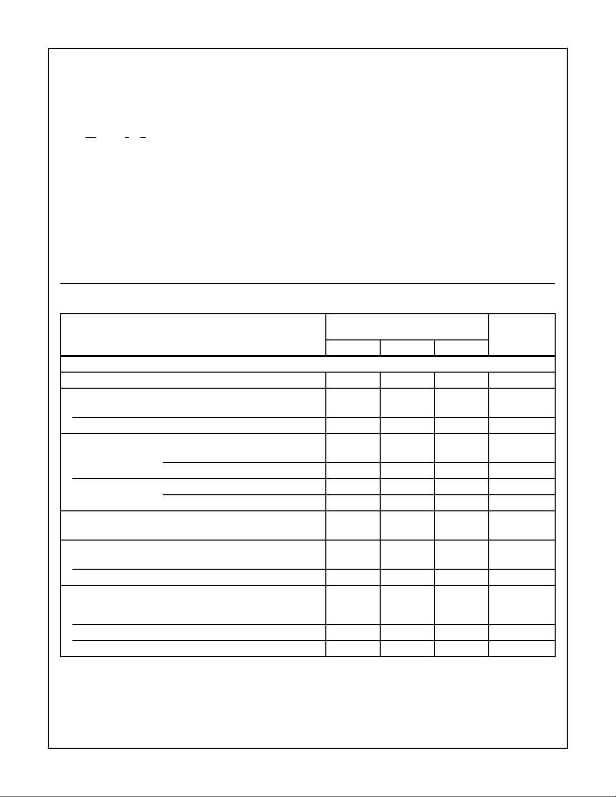
DC and Transfer Accuracy Specifications Typical at 25
Unless Otherwise Specified
PARAMETER
DYNAMIC CHARACTERISTICS
Resolution (Max) 12 12 12 Bits
Linearity Error
25oC (Max) ±1 ±1/
0oC to 75oC (Max) ±1 ±1/
Max Resolution For Which No Missing Codes Is Guaranteed
25oC HI-574A, HI-674A 12 12 12 Bits
HI-774 11 12 12 Bits
T
to T
MIN
MAX
Unipolar Offset (Max)
Adjustable to Zero ±2 ±1.5 ±1 LSB
Bipolar Offset (Max)
VIN = 0V (Adjustable to Zero) ±4 ±4 ±3 LSB
VIN = -10V ±0.15 ±0.1 ±0.1 % of FS
Full Scale Calibration Error
25oC (Max), With Fixed 50Ω Resistor From REF OUT To REF IN
(Adjustable to Zero)
T
T
MIN
MIN
to T
to T
(No Adjustment At 25oC) ±0.475 ±0.375 ±0.20 % of FS
MAX
(With Adjustment To Zero 25oC) ±0.22 ±0.12 ±0.05 % of FS
MAX
HI-574A, HI-674A 11 12 12 Bits
HI-774 11 12 12 Bits
Thermal Resistance (Typical, Note 1) θJA (oC/W) θJC (oC/W)
CLCC Package . . . . . . . . . . . . . . . . . . 65 14
SBDIP Package. . . . . . . . . . . . . . . . . . 60 18
HI3-574AxN-5, HI3-674AxN-5, HI3-774xN-5 65 N/A
Maximum Junction Temperature
HI3-574AxN-5, HI3-674AxN-5, HI3-774xN-5. . . . . . . . . . . . 150oC
HI1-574AxD-2, HI1-574AxD-5. . . . . . . . . . . . . . . . . . . . . . .175oC
HI1-674AxD-2, HI1-674AxD-5. . . . . . . . . . . . . . . . . . . . . . .175oC
HI1-774xD-2, HI1-774xD-5 . . . . . . . . . . . . . . . . . . . . . . . . .175oC
Maximum Storage Temperature Range
CC
HI3-574AxN-5, HI3-674AxN-5, HI3-774xN-5. . . . . .-40oC to 85oC
HI1-574AxD-2, HI1-574AxD-5. . . . . . . . . . . . . . . .-65oC to 150oC
HI1-674AxD-2, HI1-674AxD-5. . . . . . . . . . . . . . . .-65oC to 150oC
HI1-774xD-2, HI1-774xD-5 . . . . . . . . . . . . . . . . . .-65oC to 150oC
Maximum Lead Temperature (Soldering, 10s) . . . . . . . . . . . . 300oC
Die Characteristics
Transistor Count
HI-574A, HI-674A . . . . . . . . . . . . . . . . . . . . . . . . . . . . . . . . . 1117
HI-774 . . . . . . . . . . . . . . . . . . . . . . . . . . . . . . . . . . . . . . . . . . 2117
o
C with VCC = +15V or +12V, V
TEMPERATURE RANGE
-5 (0oC to 75oC)
2
2
±0.25 ±0.25 ±0.15 % of FS
= +5V, VEE = -15V or -12V,
LOGIC
±1/
2
±1/
2
UNITSJ SUFFIX K SUFFIX L SUFFIX
LSB
LSB
6-955
HI-574A, HI-674A, HI-774
DC and Transfer Accuracy Specifications Typical at 25
o
C with VCC = +15V or +12V, V
= +5V, VEE = -15V or -12V,
LOGIC
Unless Otherwise Specified (Continued)
TEMPERATURE RANGE
-5 (0oC to 75oC)
PARAMETER
Temperature Coefficients
Guaranteed Max Change, T
MIN
to T
(Using Internal Reference)
MAX
Unipolar Offset HI-574A, HI-674A ±2 ±1 ±1 LSB
HI-774 ±2 ±1 ±1 LSB
Bipolar Offset HI-574A, HI-674A ±2 ±1 ±1 LSB
HI-774 ±2 ±2 ±1 LSB
Full Scale Calibration HI-574A, HI-674A ±9 ±2 ±2 LSB
HI-774 ±9 ±5 ±2 LSB
Power Supply Rejection
Max Change In Full Scale Calibration
+13.5V < VCC < +16.5V or +11.4V < VCC < +12.6V ±2 ±1 ±1 LSB
+4.5V < V
< +5.5V ±1/
LOGIC
2
±1/
2
±1/
2
-16.5V < VEE < -13.5V or -12.6V < VEE < -11.4V ±2 ±1 ±1 LSB
ANALOG INPUTS
Input Ranges
Bipolar -5 to +5 V
-10 to +10 V
Unipolar 0 to +10 V
0 to +20 V
Input Impedance
10V Span 5K, ±25% Ω
20V Span 10K, ±25% Ω
POWER SUPPLIES
Operating Voltage Range
V
LOGIC
V
CC
V
EE
+4.5 to +5.5 V
+11.4 to +16.5 V
-11.4 to -16.5 V
Operating Current
I
LOGIC
7 Typ, 15 Max mA
ICC +15V Supply 11 Typ, 15 Max mA
IEE -15V Supply 21 Typ, 28 Max mA
Power Dissipation
±15V, +15V 515 Typ, 720 Max mW
±12V, +5V 385 Typ mW
Internal Reference Voltage
T
to T
MIN
MAX
Output Current, Available For External Loads (External Load Should
+10.00 ±0.05 Max V
2.0 Max mA
Not Change During Conversion).
UNITSJ SUFFIX K SUFFIX L SUFFIX
LSB
6-956
HI-574A, HI-674A, HI-774
DC and Transfer Accuracy Specifications Typical at 25
o
C with VCC = +15V or +12V, V
= +5V, VEE = -15V or -12V,
LOGIC
Unless Otherwise Specified
TEMPERATURE RANGE
-2 (-55oC to 125oC)
PARAMETER
UNITSS SUFFIX T SUFFIX U SUFFIX
DYNAMIC CHARACTERISTICS
Resolution (Max) 12 12 12 Bits
Linearity Error
25oC ±1 ±1/
2
±1/
2
-55oC to 125oC (Max) ±1 ±1 ±1 LSB
Max Resolution For Which No Missing Codes Is Guaranteed
25oC HI-574A, HI-674A 12 12 12 Bits
HI-774 11 12 12 Bits
T
MIN
to T
MAX
HI-574A, HI-674A 11 12 12 Bits
HI-774 11 12 12 Bits
Unipolar Offset (Max)
Adjustable to Zero HI-574A, HI-674A ±2 ±1.5 ±1 LSB
HI-774 ±2 ±2 ±1 LSB
Bipolar Offset (Max)
VIN = 0V (Adjustable to Zero) ±4 ±4 ±3 LSB
VIN = -10V ±0.15 ±0.1 ±0.1 % of FS
Full Scale Calibration Error
25oC (Max), With Fixed 50Ω Resistor From REF OUT To REF IN
±0.25 ±0.25 ±0.15 % of FS
(Adjustable To Zero)
T
T
MIN
MIN
to T
to T
(No Adjustment At 25oC) ±0.75 ±0.50 ±0.275 % of FS
MAX
(With Adjustment To Zero At 25oC) ±0.50 ±0.25 ±0.125 % of FS
MAX
Temperature Coefficients
Guaranteed Max Change, T
MIN
to T
(Using Internal Reference)
MAX
Unipolar Offset ±2 ±1 ±1 LSB
Bipolar Offset ±2 ±2 ±1 LSB
Full Scale Calibration ±20 ±10 ±5 LSB
Power Supply Rejection
Max Change In Full Scale Calibration
+13.5V < VCC < +16.5V or +11.4V < VCC < +12.6V ±2 ±1 ±1 LSB
+4.5V < V
< +5.5V ±1/
LOGIC
2
±1/
2
±1/
2
-16.5V < VEE < -13.5V or -12.6V < VEE < -11.4V ±2 ±1 ±1 LSB
ANALOG INPUTS
Input Ranges
Bipolar -5 to +5 V
-10 to +10 V
Unipolar 0 to +10 V
0 to +20 V
LSB
LSB
6-957
 Loading...