

Page 1
查询5962-9859101NXB供应商
TM
HI5905N/QML
Data Sheet July 1999
14-Bit, 5 MSPS, Military A/D Converter
The HI5905N/QML is a monolithic, 14-bit, 5MSPS Analogto-Digital Converter fabricated in an advanced BiCMOS
process. It is designed for high speed, high resolution
applications where wide bandwidth, low power consumption
and excellent SINAD performance are essential. With a
100MHz full power input bandwidth and high frequency
accuracy, the converter is ideal for many Military types of
communication systems employing digital IF architectures.
The HI5905N/QMLis designed in a fully differential pipelined
architecture with a front end differential-in-differential-out
sample-and-hold amplifier (S/H). Consuming 350mW (typ)
power at 5MSPS, the HI5905N/QML has excellent dynamic
performance over the full Military temperature range.
Data output latches are provided which present valid data to
the output bus with a data latency of only 4 clock cycles.
Specifications for QML devices are controlled by the
Defense Supply Center in Columbus (DSCC). The SMD
numbers listed below must be used when ordering.
Detailed Electrical Specifications for the HI5905N/QML
are contained in SMD 5962-98591. That document may
be easily downloaded from our website.
http://www.Intersil.com/data/sm/index.htm
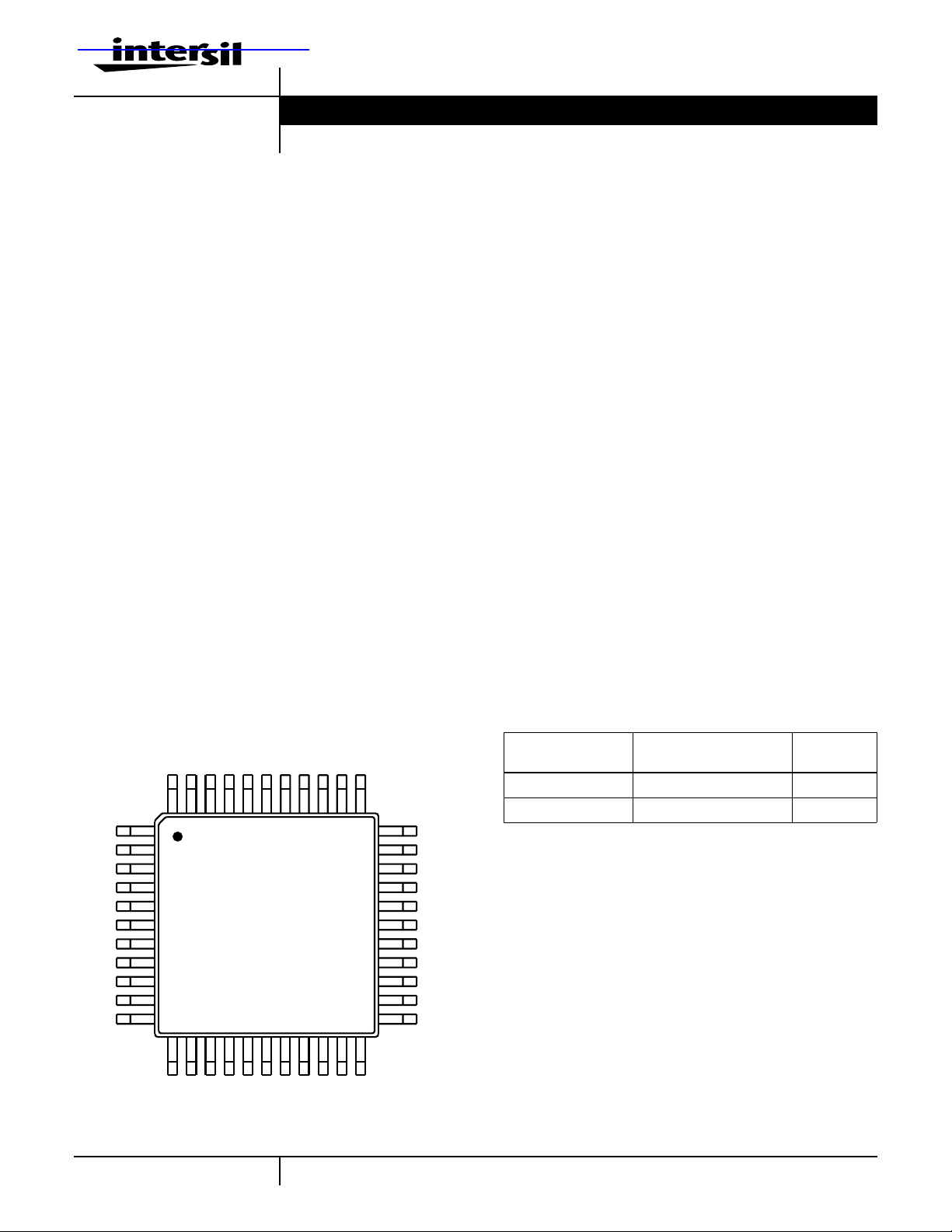
Pinout
HI5905 (MQFP) (MO-108AA-2 ISSUE A)
TOP VIEW
File Number 4718.1
Features
• QML Compliant per SMD 5962-9859101NXB
• Sampling Rate . . . . . . . . . . . . . . . . . . . . . . . . . . . .5MSPS
• Low Power at 5MSPS. . . . . . . . . . . . . . . . . 400mW (Max)
• Internal Sample and Hold
• Fully Differential Architecture
• Full Power Input Bandwidth . . . . . . . . . . . . . . . . . 100MHz
• SINAD at 1MHz . . . . . . . . . . . . . . . . . . . . . . >69dB (Min)
• Internal Voltage Reference
• TTL Compatible Clock Input
• CMOS Compatible Digital Data Outputs
Applications
• Digital Communication Systems
• Undersampling Digital IF
• Asymmetric Digital Subscriber Line (ADSL)
• Document Scanners
• Reference Literature
- AN9214, Using Intersil High Speed A/D Converters
- AN9785, Using the Intersil HI5905 EVAL2 Evaluation
Board
Ordering Information
D
NC
NC
GND1
NC
AV
A
GND
NC
NC
V
IN+
V
V
CC
IN-
DC
CC1
CC1
GND1
NC
DV
DV
D
44 43 42 41 40
1
2
3
4
5
6
7
8
9
10
11
12 13 14 15 16 17
NC
RIN
GND
V
ROUT
A
V
4-1
CLKNCD0D1D2NCNC
39 38 37 36 35 34
CC
NC
D13
AV
D12
D11
2221201918
D10
33
32
31
30
29
28
27
26
25
24
23
NC
ORDERING
NUMBER
INTERNAL INTERSIL
MKT. NUMBER
TEMP.
RANGE(oC)
5962-9859101NXB HI5905N/QML -55 to 125
HI5905EVAL2 Low Frequency Platform 25
D3
D4
D5
D6
D7
NC
DV
CC2
D
GND2
D8
D9
NC
CAUTION: These devices are sensitive to electrostatic discharge; follow proper IC Handling Procedures.
1-888-724-7143
| Copyright © Intersil Corporation 1999
Page 2
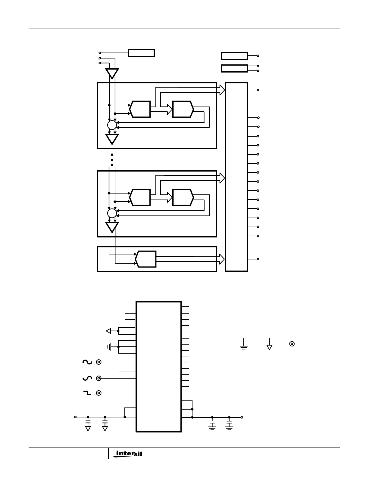
Functional Block Diagram
V
DC
V
IN
VIN+
-
BIAS
S/H
CLOCK
REF
CLK
V
ROUT
V
RIN
STAGE 1
DV
CC2
X8
4-BIT
FLASH
+
-
∑
4-BIT
DAC
D13 (MSB)
D12
D11
D10
D9
STAGE 4
D8
D7
X8
AND
4-BIT
FLASH
4-BIT
DAC
+
-
∑
DIGITAL DELAY
DIGITAL ERROR CORRECTION
D6
D5
D4
D3
D2
D1
D0 (LSB)
STAGE 5
AV
CCAGNDDVCC1DGND1
Typical Application Schematic
+
V
IN
VIN-
CLOCK
+5V
10µF
+
0.1µF
4-BIT
FLASH
V
ROUT
V
(14)
RIN
A
(6)
GND
A
(15)
GND
D
GND1
D
GND1
D
GND2
VIN+ (9)
VDC (11)
V
- (10)
IN
(MSB) D13 (18)
CLK (40)
AVCC (5)
AV
(16)
CC
(LSB) D0 (38)
D1 (37)
(13)
D2 (36)
D3 (33)
D4 (32)
D5 (31)
(3)
D6 (30)
(42)
D7 (29)
(26)
D8 (25)
D9 (24)
D10 (21)
D11 (20)
D12 (19)
DV
CC1
DV
(43)
CC1
(27)
DV
CC2
(41)
D0
D1
D2
D3
D4
D5
D6
D7
D8
D9
D10
D11
D12
D13
0.1µF
D
GND2
D
GND
A
GND
BNC
10µF AND 0.1µF CAPS ARE PLACED
AS CLOSE TO PART AS POSSIBLE
+5V
+
10µF
4-2
HI5905
Page 3
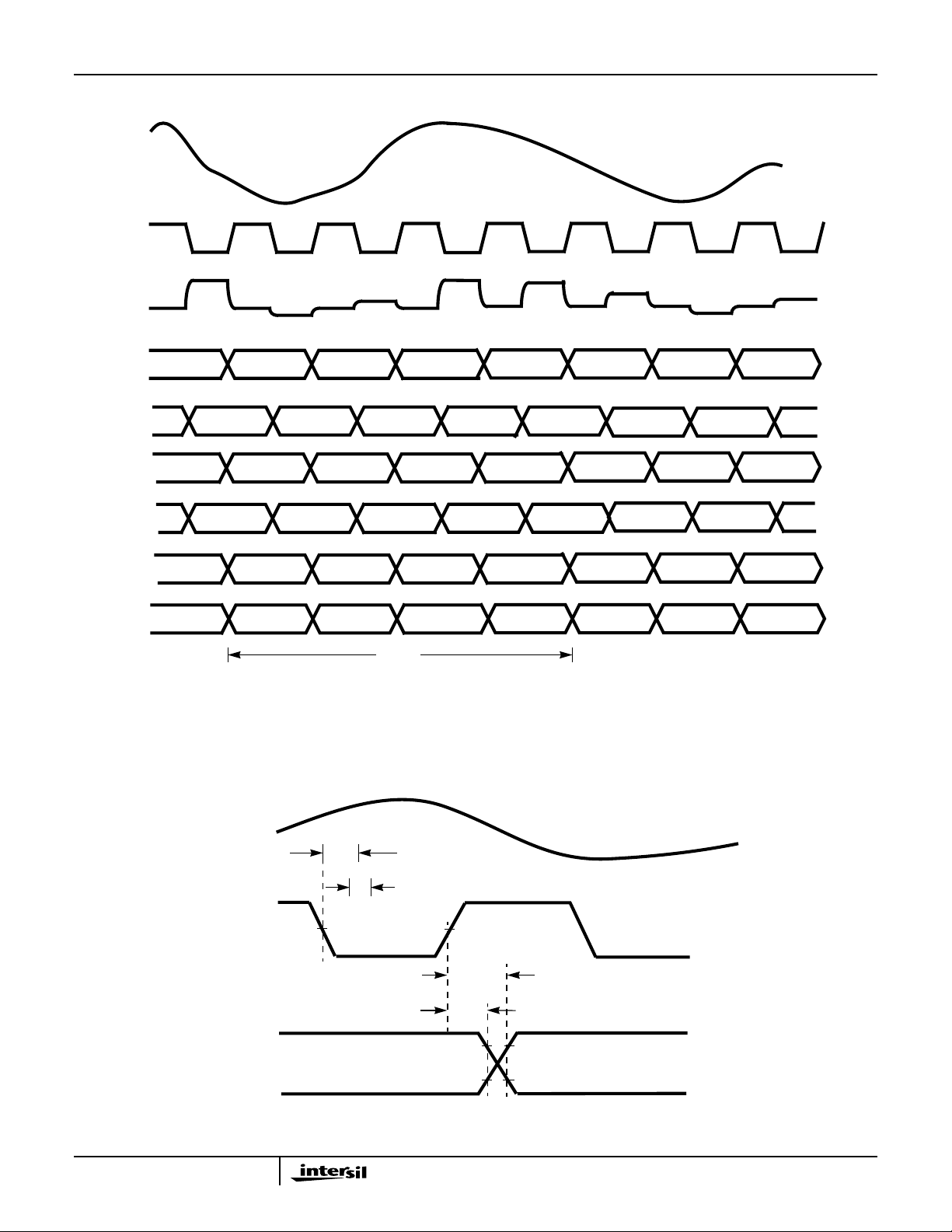
Timing Waveforms
ANALOG
INPUT
CLOCK
INPUT
S
N - 1HN - 1SN
INPUT
S/H
1ST
STAGE
2ND
STAGE
B2,
3RD
STAGE
4TH
STAGE
B4,
5TH
STAGE
DAT A
OUTPUT
NOTES:
1. SN: N-th sampling period.
2. HN: N-th holding period.
N - 2
N - 3
B1,
B3,
B
5, N - 3
D
N - 1
N - 2
N - 4
HNS
N + 1HN + 1SN + 2HN + 2SN + 3HN + 3SN + 4HN + 4SN + 5HN + 5SN + 6HN + 6
B2,
B4,
N - 1
N - 2
B
B3,
B5,
D
1, N
N - 1
N - 2
N - 3
B2,
B4,
t
LAT
N
N - 1
B
1, N + 1
B3,
B5,
D
N
N - 1
N - 2
B2,
B4,
N + 1
N
B
B3,
B5,
3. B
B
N + 2
N + 1
1, N + 3
B3,
B5,
D
N + 2
N + 1
N
1, N + 2
B2,
N + 1
B4,
N
D
N - 1
:M-thstage digital output corresponding to N-th sampledinput.
M, N
B2,
B4,
N + 3
N + 2
B
1, N + 4
B3,
B5,
D
B2,
N + 3
B4,
N + 2
N + 1
4. DN: Final data output corresponding to N-th sampled input.
FIGURE 1. INTERNAL CIRCUIT TIMING
N + 4
N + 3
B
1, N + 5
B3,
B5,
D
N + 4
N + 3
N + 2
ANALOG
INPUT
CLOCK
INPUT
DAT A
OUTPUT
4-3
1.5V
t
AP
t
AJ
1.5V
t
OD
t
H
3.5V
DATA N-1 DATA N
1.5V
FIGURE 2. INPUT-TO-OUTPUT TIMING
Page 4

Pin Descriptions
PIN # NAME DESCRIPTION
1 NC No Connection
2 NC No Connection
3D
4 NC No Connection
5AVCCAnalog Supply (5.0V)
6A
7 NC No Connection
8 NC No Connection
9V
10 VIN- Negative Analog Input
11 V
12 NC No Connection
13 V
14 V
15 A
16 AV
17 NC No Connection
18 D13 Data Bit 11 Output (MSB)
19 D12 Data Bit 11 Output
20 D11 Data Bit 11 Output
21 D10 Data Bit 10 Output
22 NC No Connection
23 NC No Connection
24 D9 Data Bit 9 Output
25 D8 Data Bit 8 Output
26 D
27 DV
28 NC No Connection
29 D7 Data Bit 7 Output
30 D6 Data Bit 6 Output
31 D5 Data Bit 5 Output
32 D4 Data Bit 4 Output
33 D3 Data Bit 3 Output
34 NC No Connection
35 NC No Connection
36 D2 Data Bit 2 Output
37 D1 Data Bit 1 Output
38 D0 Data Bit 0 Output (LSB)
39 NC No Connection
40 CLK Input Clock
41 DV
42 D
43 DV
44 NC No Connection
GND1
GND
IN
DC
ROUT
RIN
GND
GND2
GND1
Digital Ground
Analog Ground
+ Positive Analog Input
DC Bias Voltage Output
Reference Voltage Output
Reference Voltage Input
Analog Ground
Analog Supply (5.0V)
CC
Digital Ground
Digital Supply (5.0V)
CC2
Digital Supply (5.0V)
CC1
Digital Ground
Digital Supply (5.0V)
CC1
Detailed Description
Theory of Operation
The HI5905 is a 14-bit fully differential sampling pipeline A/D
converter with digital error correction. Figure 3 depicts the
circuit for the front end differential-in-differential-out sampleand-hold (S/H). The switches are controlled by an internal
clock which is a non-overlapping two phase signal, φ
φ
, derived from the master clock. During the sampling
2
phase, φ
capacitors, C
, the input signal is applied to the sampling
1
. At the same time the holding capacitors, CH,
S
are discharged to analog ground. At the falling edge of φ
the input signal is sampled on the bottom plates of the
sampling capacitors. In the next clock phase, φ
bottom plates of the sampling capacitors are connected
together and the holding capacitors are switched to the op
amp output nodes. The charge then redistributes between
C
and CH completing one sample-and-hold cycle. The
S
output is a fully-differential, sampled-data representation of
the analog input. The circuit not only performs the sampleand-hold function but will also convert a single-ended input
to a fully-differential output for the converter core. During the
sampling phase, the V
switch and C
. The relatively small values of these
S
pins see only the on-resistance of a
IN
components result in a typical full power input bandwidth of
100MHz for the converter.
φ
1
φ
1
C
VIN+
V
-
IN
FIGURE 3. ANALOG INPUT SAMPLE-AND-HOLD
S
φ
2
C
S
φ
1
φ
1
-
+ -
+
φ
C
C
1
H
H
φ
1
As illustrated in the functional block diagram and the timing
diagram in Figure 1, four identical pipeline subconverter
stages, each containing a four-bit flash converter, a four-bit
digital-to-analog converter and an amplifier with a voltage
gain of 8, follow the S/H circuit with the fifth stage being only
a 4-bit flash converter. Each converter stage in the pipeline
will be sampling in one phase and amplifying in the other
clock phase. Each individual sub-converter clock signal is
offset by 180 degrees from the previous stage clock signal,
with the result that alternate stages in the pipeline will
perform the same operation.
The output of each of the four-bit subconverter stages is a
four-bit digital word containing a supplementary bit to be
used by the digital error correction logic. The output of each
subconverter stage is input to a digital delay line which is
controlled by the internal sampling clock. The function of the
digital delay line is to time align the digital outputs of the four
, the two
2
V
OUT
V
OUT
and
1
+
-
1
4-4
Page 5

identical four-bit subconverter stages with the corresponding
output of the fifth stage flash converter before applying the
twenty bit result to the digital error correction logic. The
digital error correction logic uses the supplementary bits to
correct any error that may exist before generating the final
fourteen bit digital data output of the converter.
Because of the pipeline nature of this converter, the digital
data representing an analog input sample is output to the
digital data bus on the 4th cycle of the clock after the analog
sample is taken. This time delay is specified as the data
latency. After the data latency time, the digital data
representing each succeeding analog sample is output
during the following clock cycle. The digital output data is
synchronized to the external sampling clock with a latch. The
digital output data is available in two’s complement binary
format (see Table 1, A/D Code Table).
Internal Reference Generator, V
ROUT
and V
RIN
The HI5905 has an internal reference generator, therefore, no
external reference voltage is required. V
connected to V
when using the internal reference voltage.
RIN
ROUT
must be
The HI5905 can be used with an external reference. The
converter requires only one external reference voltage
connected to the V
The HI5905 is tested with V
to V
. Internal to the converter, two reference voltages of
RIN
pin with V
RIN
left open.
ROUT
, equal to 4.0V, connected
ROUT
1.3V and 3.3V are generated for a fully differential input
signal range of ±2V.
In order to minimize overall converter noise, it is
recommended that adequate high frequency decoupling be
provided at the reference voltage input pin, V
RIN
.
Analog Input, Differential Connection
The analog input to the HI5905 can be configured in various
ways depending on the signal source and the required level
of performance. A fully differential connection (Figure 4) will
give the best performance for the converter.
Since the HI5905 is powered off a single +5V supply, the
analog input must be biased so it lies within the analog input
common mode voltage range of 1.0V to 4.0V. The
performance of the ADC does not change significantly with
the value of the analog input common mode voltage.
V
IN
-V
IN
FIGURE 4. AC COUPLED DIFFERENTIAL INPUT
A 2.3V DC bias voltage source, V
DC
VIN+
HI5905
V
DC
VIN-
, half way between the
top and bottom internal reference voltages, is made
available to the user to help simplify circuit design when
using a differential input. This low output impedance voltage
source is not designed to be a reference but makes an
excellent bias source and stays within the analog input
common mode voltage range over temperature.
The difference between the con v erter’s tw o internal voltage
references is 2V. For the A C coupled diff erential input,(Figure
4), if V
phase with V
bias voltage equal to V
on a DC bias voltage equal to V
IN
is a 2V
P-P
, then VIN+ is a 2V
IN
sinewav ewith -VINbeing180 degrees out of
sinewav e riding on a DC
P-P
and VIN- is a 2V
DC
. Consequently ,theconverter
DC
sinewav e riding
P-P
will be at positive full scale,resulting in a digital data output code
with D13 (MSB) equal to a logic “0” and D0-D12 equal to logic
“1” (see Table 1, A/D Code Table), when the V
V
+1V and the VIN- input is at VDC-1V (VIN+- VIN- = 2V).
DC
+ input is at
IN
Conversely, the ADC will be at negative full scale, resulting in a
digital data output code with D13 (MSB) equal to a logic “1” and
D0-D12 equal to logic “0” (see Table 1, A/D Code Table), when
the V
+ input is equal to VDC-1V and VIN- is at VDC+1V
IN
(V
+-VIN- = -2V). From this, the con v erter is seen to hav e a
IN
peak-to-peak differential analog input v oltage range of 2V.
The analog input can be DC coupled (Figure 5) as long as
the inputs are within the analog input common mode voltage
range (1.0V ≤ VDC ≤ 4.0V).
TABLE 1. A/D CODE TABLE
DIFFERENTIAL
CODE
CENTER
DESCRIPTION
+Full Scale
(+FS) - 1/4 LSB
+FS - 1 1/4 LSB 1.99969V 0 1 1 1 1 1 1 1 1 1 1 1 1 0
+ 3/4 LSB 183.105µV 00000000000000
- 1/4 LSB -61.035µV 11111111111111
-FS + 1 3/4 LSB -1.99957V 1 0 0 0 0 0 0 0 0 0 0 0 0 1
-Full Scale
(-FS) + 3/4 LSB
INPUTVOLTAGE
(USING INTERNAL
REFERENCE)
+1.99994V 0 1 1 1 1 1 1 1 1 1 1 1 1 1
-1.99982V 1 0 0 0 0 0 0 0 0 0 0 0 0 0
†
MSB LSB
D13 D12 D11 D10 D9 D8 D7 D6 D5 D4 D3 D2 D1 D0
TWO’S COMPLEMENT BINARY OUTPUT CODE
† The voltages listed above represent the ideal center of each two’s complement binary output code shown.
4-5
Page 6

V
IN
VDC
R
-V
IN
VDC
FIGURE 5. DC COUPLED DIFFERENTIAL INPUT
R
VIN+
V
DC
VIN-
HI5905
C
The resistors, R, in Figure 5 are not absolutely necessary
but may be used as load setting resistors. A capacitor, C,
connected from V
+ to VIN- will help filter any high
IN
frequency noise on the inputs, also improving performance.
Values around 20pF are sufficient and can be used on AC
coupled inputs as well. Note, however, that the value of
capacitor C chosen must take into account the highest
frequency component of the analog input signal.
Analog Input, Single-Ended Connection
The configuration shown in Figure 6 may be used with a
single ended AC coupled input. Sufficient headroom must
be provided such that the input voltage never goes above
+5V or below A
GND
.
The resistor, R, in Figure 7 is not absolutely necessary but
may be used as a load setting resistor . A capacitor, C,
connected from V
+toVIN- will help filter any high frequency
IN
noise on the inputs, also improving performance. Values
around 20pF are sufficient and can be used on AC coupled
inputs as well. Note, howe ver, that the value of capacitor C
chosen must take into account the highest frequency
component of the analog input signal.
A single ended source will give better overall system
performance if it is first converted to differential before
driving the HI5905.
Digital I/O and Clock Requirements
The HI5905 provides a standard high-speed interface to
external TTL/CMOS logic families. The digital CMOS clock
input has TTL level thresholds. The low input bias current
allows the HI5905 to be driven by CMOS logic. The digital
CMOS outputs have a separate +5.0V digital supply input pin.
In order to ensure rated performance of the HI5905, the duty
cycle of the clock should be held at 50% ±5%. It must also
have low jitter and operate at standard TTL levels.
Performance of the HI5905 will only be guaranteed at
conversion rates above 0.5MSPS. This ensures proper
performance of the internal dynamic circuits.
V
IN
VDC
FIGURE 6. AC COUPLED SINGLE ENDED INPUT
VIN+
HI5905
VIN-
Again, the difference between the two internal voltage
references is 2V. If V
4V
sinewav eriding on a positive voltage equal to VDC. The
P-P
converter will be at positivefull scale when V
(V
+ - VIN- = 2V) and will be at negative full scale when VIN+
IN
is equal to VDC - 2V (V
is a 4V
IN
+ - VIN- = -2V). In this case, VDC
IN
sinewav e , then VIN+ is a
P-P
+isatVDC+2V
IN
could range between 2V and 3V without a significant change in
ADC performance. The simplest way to produce VDC is to use
the V
bias voltage output of the HI5905.
DC
The single ended analog input can be DC coupled (Figure 7)
as long as the input is within the analog input common mode
voltage range.
V
IN
VDC
R
VDC
FIGURE 7. DC COUPLED SINGLE ENDED INPUT
VIN+
C
HI5905
VIN-
Supply and Ground Considerations
The HI5905 has separate analog and digital supply and ground
pins to keepdigital noise out of the analog signal path. The part
should be mounted on a board that provides separate low
impedance connections for the analog and digital supplies and
grounds. For best perf ormance, the supplies to the HI5905
should be driven by clean, linear regulated supplies. The board
should also have good high frequency decoupling capacitors
mounted as close as possible to the converter . If the part is
powered off a single supply then the analog supply and ground
pins should be isolated by ferrite beads from the digital supply
and ground pins.
Refer to the Application Note AN9214, “Using Intersil High
Speed A/D Converters” for additional considerations when
using high speed converters.
Static Performance Definitions
Offset Error (VOS)
The midscale code transition should occur at a level 1/4 LSB
above half-scale. Offset is defined as the deviation of the
actual code transition from this point.
Full-Scale Error (FSE)
The last code transition should occur foran analog input that
is 3/4 LSB below positive full-scale with the offset error
removed. Full-scale error is defined as the deviation of the
actual code transition from this point.
Differential Linearity Error (DNL)
DNL is the worst case deviation of a code width from the
ideal value of 1 LSB.
4-6
Page 7

Integral Linearity Error (INL)
INL is the worst case deviation of a code center from a best
fit straight line calculated from the measured data.
Power Supply Rejection Ratio (PSRR)
Each of the power supplies are moved plus and minus 5%
and the shift in the offset and gain error (in LSBs) is noted.
Dynamic Performance Definitions
Fast F ourier Transform (FFT) techniques are used to ev aluate
the dynamic performance of the HI5905. A low distortion sine
wave is applied to the input, it is coherently sampled, and the
output is stored in RAM. The data is then transformed into the
frequency domain with an FFT and analyzed to evaluate the
dynamic performance of the A/D . The sine wa ve input to the
part is -0.5dB down from full-scale for all these tests. SNR and
SINAD are quoted in dB. The distortion numbers are quoted in
dBc (decibels with respect to carrier) and DO NOT include any
correction factors for normalizing to full scale.
Signal-to-Noise Ratio (SNR)
SNR is the measured RMS signal to RMS noise at a
specified input and sampling frequency. The noise is the
RMS sum of all of the spectral components except the
fundamental and the first five harmonics.
Signal-to-Noise + Distortion Ratio (SINAD)
SINAD is the measured RMS signal to RMS sum of all
other spectral components below the Nyquist frequency,
f
/2, excluding DC.
S
Effective Number Of Bits (ENOB)
The effective number of bits (ENOB) is calculated from the
SINAD data by:
ENOB = SINAD + V
where: V
V
CORR
fullscale.
= 0.5dB (Typical)
CORR
adjusts the ENOB for the amount the input is below
Total Harmonic Distortion (THD)
THD is the ratio of the RMS sum of the first 5 harmonic
components to the RMS value of the fundamental input signal.
2nd and 3rd Harmonic Distortion
This is the ratio of the RMS value of the applicable harmonic
component to the RMS value of the fundamental input signal.
Spurious Free Dynamic Range (SFDR)
SFDR is the ratio of the fundamental RMS amplitude to the
RMS amplitude of the next largest spur or spectral
component (excluding the first 5 harmonic components) in
the spectrum below f
Intermodulation Distortion (IMD)
Nonlinearities in the signal path will tend to generate
intermodulation products when two tones, f
CORR
/2.
S
-1.76()/6.02
and f2, are
1
present at the inputs. The ratio of the measured signal to the
distortion terms is calculated. The terms included in the
calculation are (f
(f
+ 2f2), (f1- 2f2). The ADC is tested with each tone 6dB
1
below full scale.
), (f1-f2), (2f1), (2f2), (2f1+f2), (2f1-f2),
1+f2
Transient Response
Transient response is measured by providing a fullscale
transition to the analog input of the ADC and measuring the
number of cycles it takes for the output code to settle within
14-bit accuracy.
Over-Voltage Recovery
Over-voltage Recovery is measured by providing a fullscale
transition to the analog input of the ADC which overdrives
the input by 200mV, and measuring the number of cycles it
takes for the output code to settle within 14-bit accuracy.
Full Power Input Bandwidth (FPBW)
Full power input bandwidth is the analog input frequency at
which the amplitude of the digitally reconstructed output has
decreased 3dB below the amplitude of the input sinewave.
The input sinewave has an amplitude which swings from -f
to +fS. The bandwidth given is measured at the specified
sampling frequency.
Timing Definitions
Refer to Figure 1, Internal Circuit Timing, and Figure 2,
Input-To-Output Timing, for these definitions.
Aperture Delay (tAP)
Aperture delay is the time delay between the external
sample command (the falling edge of the clock) and the time
at which the signal is actually sampled. This delay is due to
internal clock path propagation delays.
Aperture Jitter (tAJ)
Aperture Jitter is the RMS variation in the aperture delay due
to variation of internal clock path delays.
Data Hold Time (tH)
Data hold time is the time to where the previous data (N - 1)
is still valid.
Data Output Delay Time (tOD)
Data output delay time is the time to where the new data (N)
is valid.
Data Latency (t
After the analog sample is taken, the digital data is output on
the bus at the third cycle of the clock. This is due to the
pipeline nature of the converter where the data has to ripple
through the stages. This delay is specified as the data
latency. After the data latency time, the data representing
each succeeding sample is output at the following clock
pulse. The digital data lags the analog input sample by 4
clock cycles.
LAT
)
S
4-7
Page 8

HI5905N/QML
Metric Plastic Quad Flatpack Packages (MQFP/PQFP)
E
E1
0.40
0.016
0o MIN
0o-7
-H-
-A-
o
MIN
D
D1
-D-
Q44.10x10 (JEDEC MO-108AA-2 ISSUE A)
44 LEAD METRIC PLASTIC QUAD FLATPACK PACKAGE
SYM-
BOL
INCHES MILLIMETERS
NOTESMIN MAX MIN MAX
A - 0.093 - 2.35 -
A1 0.004 0.010 0.10 0.25 -
-B-
A2 0.077 0.083 1.95 2.10 -
B 0.012 0.018 0.30 0.45 6
B1 0.012 0.016 0.30 0.40 -
D 0.510 0.530 12.95 13.45 3
D1 0.390 0.398 9.90 10.10 4, 5
E 0.510 0.530 12.95 13.45 3
e
PIN 1
E1 0.390 0.398 9.90 10.10 4, 5
L 0.026 0.037 0.65 0.95 N44 447
e 0.032 BSC 0.80 BSC -
5o-16
A2
SEATING
PLANE
A
0.10
o
A1
0.20
0.008
A-B SD SCM
0.004
-C-
B
B1
NOTES:
1. Controlling dimension: MILLIMETER. Converted inch
dimensions are not necessarily exact.
2. All dimensions and tolerances per ANSI Y14.5M-1982.
3. Dimensions D andE to be determined at seating plane .
4. Dimensions D1 and E1 to be determined at datum plane
.
-H-
5. Dimensions D1 and E1 do not include mold protrusion.
Rev. 1 1/94
-C-
Allowable protrusion is 0.25mm (0.010 inch) per side.
0.13/0.17
o
L
5o-16
0.005/0.007
BASE METAL
WITH PLATING
0.13/0.23
0.005/0.009
6. Dimension B does not include dambar protrusion. Allowable
dambar protrusion shall be 0.08mm (0.003 inch) total.
7. “N” is the number of terminal positions.
All Intersil semiconductor products are manufactured, assembled and tested under ISO9000 quality systems certification.
Intersil semiconductor products are sold by description only. Intersil Corporation reserves the right to make changes in circuit design and/or specifications at any time without notice. Accordingly ,the reader is cautioned to verify that data sheets are current before placing orders. Information furnished by Intersil is believed to be accurate and
reliable. However, no responsibility is assumed by Intersil or its subsidiaries for its use; nor for any infringements of patents or other rights of third parties which may result
from its use. No license is granted by implication or otherwise under any patent or patent rights of Intersil or its subsidiaries.
For information regarding Intersil Corporation and its products, see web site www.intersil.com
Sales Office Headquarters
NORTH AMERICA
Intersil Corporation
P. O. Box 883, Mail Stop 53-204
Melbourne, FL 32902
TEL: (321) 724-7000
FAX: (321) 724-7240
4-8
EUROPE
Intersil SA
Mercure Center
100, Rue de la Fusee
1130 Brussels, Belgium
TEL: (32) 2.724.2111
FAX: (32) 2.724.22.05
ASIA
Intersil Ltd.
8F-2, 96, Sec. 1, Chien-kuo North,
Taipei, Taiwan 104
Republic of China
TEL: 886-2-2515-8508
FAX: 886-2-2515-8369
 Loading...