

Page 1
TM
HI5905EVAL2 Evaluation Board User’s Manual
Application Note January 1999
Description
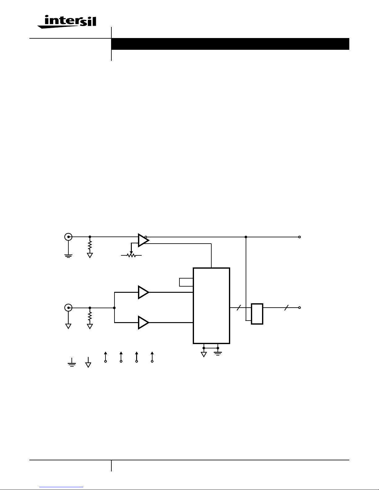
The HI5905EV AL2 evaluation board allows the circuit
designer to evaluate the performance of the Intersil HI5905
monolithic 14-bit, 5MSPS analog-to-digital converter (ADC).
As shown in the Evaluation Board Functional Block Diagr am,
the evaluation board includes sample cloc k gener ation
circuitry, a single-ended to differential analog input amplifier
configuration and digital data output latches/buffers . The
buffered digital data outputs are conveniently provided for
easy interfacing to a ribbon connector or logic probes. In
addition, the evaluationboardincludessomeprototypingarea
for the addition of user designed custom interfaces or circuits .
The sample clock generator circuit accepts the external
sampling signal through anSMAtypeRFconnector, J2. This
input is AC-coupled and terminated in 50Ω allowing for
connection to most laboratory signal generators. In addition,
the duty cycle of the clock driving the A/D converter is
Evaluation Board Functional Block Diagram
AN9785
adjustable by way of a potentiometer. This allows the effects
of sample clock duty cycle on the HI5905 to be observed.
The analog input signal is also connected through an SMA
type RF connector, J1, and applied to a single-ended to
differential analog input amplifier. This input is AC-coupled
and terminated in 50Ω allowing for connection to most
laboratory signal generators. Also, provisions for a
differential RC lowpass filter is incorporated on the output of
the differential amplifier to limit the broadband noise going
into the HI5905 converter.
The digital data output latches/buffers consist of a pair of
74ALS574A D-type flip-flops. With this digital output
configuration the digital output data transitions seen at the
I/O connector are essentially time aligned with the rising
edge of the sampling clock.
CLK IN
J2
ANALOG
J1
DGND
TTL COMPARATOR
CLOCK
50Ω
-5V
D
IN
50Ω
AGND
+5V
-5V
D
D
+5V
G = +1
G = -1
+5VA-5V
D
CLK
V
REFOUT
V
REFIN
V
IN+
0-D13
14
D>Q
D
V
IN-
HI5905
A
14
OUT
(CLK)
DIGITAL
DAT A
OUT
(D0 - D13)
1-888-INTERSIL or 321-724-7143 | Intersil and Design is a trademark of Intersil Corporation. | Copyright © Intersil Corporation 2000
3-1
Page 2
Application Note 9785
Reference Generator, V
ROUT
and V
RIN
The HI5905 has an internal reference voltage generator,
therefore no external reference voltage is required. The eval
board, however, offers the ability to use the internal or an
external reference.V
must be connected to V
ROUT
RIN
when
using the internal reference. Internal to the converter, two
reference voltages of 1.3V and 3.3V are generated making
for a fully differential analog input signal range of
±2V.
The HI5905 can be used with an external reference. The
converter requires only one external reference voltage
connected to the V
evaluation board is configured with V
pin with V
RIN
left open. The
ROUT
ROUT
connected to V
RIN
through a 0Ωresistor , R4. If it is desired to e v aluate the
performance of the converter utilizing an externally provided
reference voltage, R4 can be remo v ed and the alternate
referencevoltagecanbebrought in through twisted pair wire or
coaxial cable. The latter would be the recommended method
since it would provide the greatest immunity to e xternally
coupled noise voltages. In order to minimize overall converter
noise it is recommended that adequate high frequency
decoupling be provided at the reference input pin, V
RIN
.
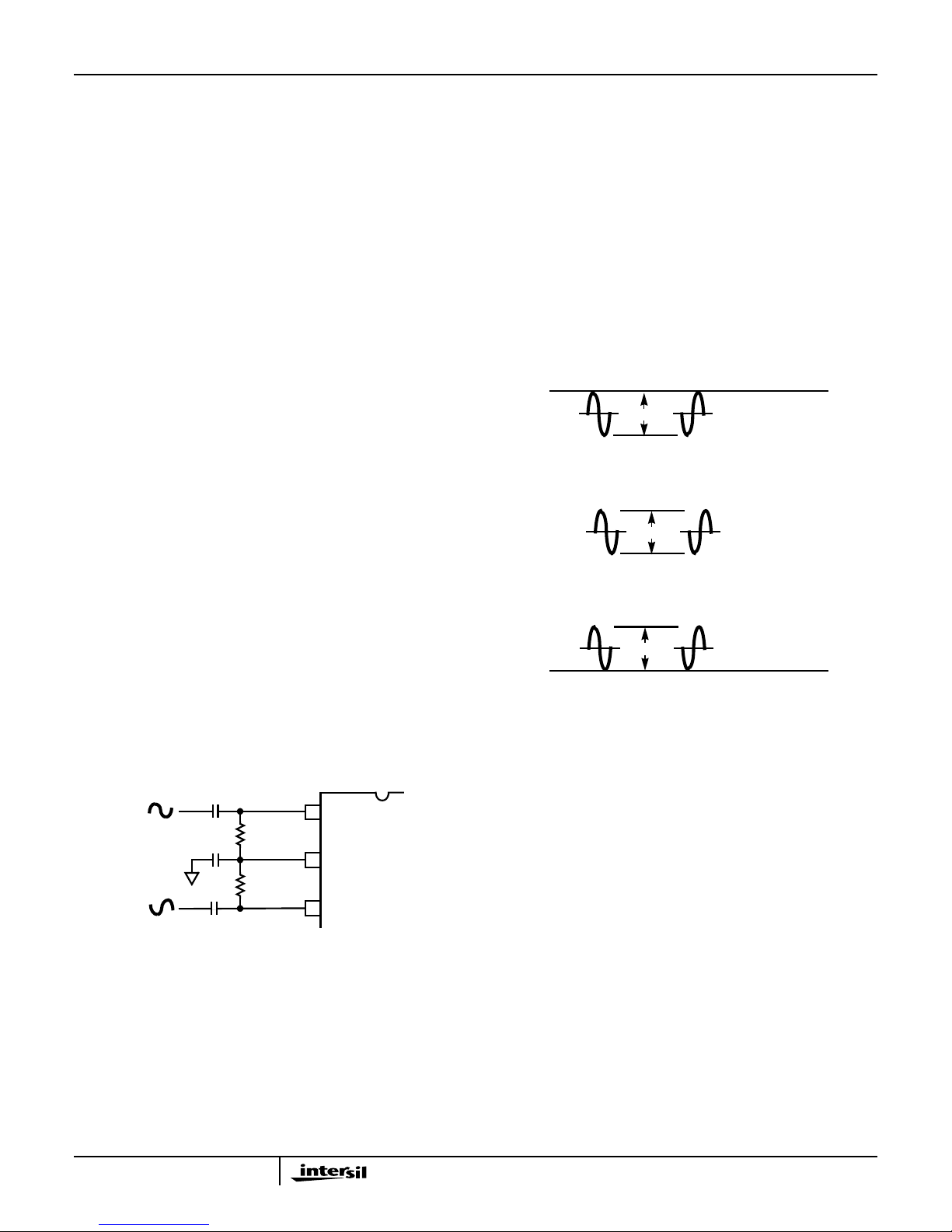
Analog Input
The fully differential analog input of the HI5905 A/D can be
configured in various ways depending on the signal source
and the required level of performance.
The difference between the conv erter's two internally
generated voltage references is 2V. For the AC coupled
differentialinput(Figure1),ifV
IN
is a 2V
sinewav ewith-V
P-P
being 180 degrees out of phase with VIN, the converter will be
at positivefullscalewhen the V
V
- input is at VDC - 1V (VIN+ - VIN- = +2V). Conversely, the
IN
ADC will be at negative full scale when the V
to V
- 1V and VIN- is at VDC + 1V (VIN+ - VIN- = -2V).
DC
+ input isatVDC+ 1Vandthe
IN
+ input is equal
IN
It should be noted that overdriving the analog input beyond
the ±2.0V fullscale input voltage range will not damage the
converter as long as the overdrive voltage stays within the
converters analog supply voltages. In the event of an
overdrive condition the converter will recover within one
sample clock cycle.
+5V
VIN+V
VIN+
2.0V
2.0V
P-P
FIGURE 2A.
P-P
FIGURE 2B.
-
IN
VDC = 4.0V
V
-
IN
1.0V < VDC < 4.0V
+5V
IN
Differential Analog Input Configuration
A fully differential connection (Figure 1) will yield the best
performance from the HI5905 A/D converter. Since the HI5905
is powered off a single +5V supply, the analog input must be
biased so it lies within the analog input common mode voltage
range of 1.0V to 4.0V .Figure2illustratesthedifferentialanalog
input common mode voltage range that the conv erter will
accommodate. The performance of the ADC does not change
significantly with the value of the common mode voltage.
V
IN
-V
IN
FIGURE 1. AC COUPLED DIFFERENTIAL INPUT
A 2.3V DC bias voltage source, V
DC
and bottom internally generated reference voltages, is made
availableto the user to help simplify circuit design when using a
differential input. This low output impedance voltage source is
not designed to be a reference but makes an excellent bias
source and stays within the analog input common mode
voltage range ov er temperature . The DC v oltage source has a
temperature coefficient of about +200ppm/
VIN+
HI5905
V
DC
VIN-
, half way between the top
o
C.
+
V
IN
2.0V
P-P
0V
FIGURE 2C.
FIGURE 2. DIFFERENTIAL ANALOG INPUT COMMON MODE
VOLTAGE RANGE
V
-
IN
VDC = 1.0V
0V
Evaluation Board Layout and
Power Supplies
The HI5905 evaluation board is a four layer board with a
layout optimized for the best performance of the ADC. This
application note includes an electrical schematic of the
evaluation board, a component parts list, a component
placement layout drawing and reproductions of the various
board layers used in the board stack-up. The user should
feel free to copy the layout in their application. Refer to the
component layout and the evaluation board electrical
schematic for the following discussions.
The HI5905 monolithic A/D converter has been designed
with separate analog and digital supply and ground pins to
keep digital noise out of the analog signal path. The
evaluation board provides separate low impedance analog
and digital ground planes on layer 2. Since the analog and
digital ground planes are connected together at a single
point where the power supplies enter the board, DO NOT tie
them together back at the power supplies.
3-2
Page 3
Application Note 9785
The analog and digital supplies are also kept separate on
the evaluation board and should be driven by clean linear
regulated supplies. The external power supplies are hooked
up with the twisted pair wires soldered to the plated through
holes marked +5VAIN, +5VAIN1, -5VAIN, +5VDIN,
+5VD1IN, +5VD2IN, -5VDIN, AGND and DGND near the
analog prototyping area. +5VDIN, +5VD1IN, +5VD2IN
and -5VDIN are digital supplies and are returned to DGND.
+5VAIN, +5VAIN1 and -5VAIN are the analog supplies and
are returned to AGND. Table 1 lists the operational supply
voltages, typical current consumption and the evaluation
board circuit function being powered. Single supply
operation of the converter is possible but the overall
performance of the converter may degrade.
TABLE 1. HI5905EVAL2EVALUATION BOARDPOWER
SUPPLIES
POWER
SUPPLY
+5VAIN 5.0V ±5% 80mA Op Amps, A/D AV
-5VAIN -5.0V ±5% 30mA Op Amps
+5VDIN 5.0V ±5%3 60mA CLK Comparator,
+5VD1IN 5.0V ±5% 14mA A/D DV
+5VD2IN 5.0V ±5% 6mA A/D DV
-5VDIN -5.0V ±5% 3mA CLK
NOMINAL
VALUE
CURRENT
(TYP)
FUNCTION(S)
SUPPLIED
CC
Inverter
D0-D13 D-FF’s
CC1
CC2
Comparator
Sample Clock Driver, Timing and I/O
In order to ensure rated performance of the HI5905, the duty
cycle of the sample clock should be held at 50% ±5%. It
must also have low phase noise and operate at standard
TTL levels.
A voltage comparator (U3) with TTL output levelsisprovided
on the evaluation board to generate the sampling clock for
the HI5905 when a sinewave (< ±3V) or squarewave clock is
applied to the CLK input (J2) of the evaluation board. A
potentiometer (VR1) is provided to allow the user to adjust
the duty cycle of the sampling clock to obtain the best
performance from the ADC and to allow the user to
investigate the effects of expected duty cycle variations on
the performance of the converter. The HI5905 clock input
trigger level is approximately 1.5V. Therefore, the duty cycle
of the sampling clock should be measured at this 1.5V
trigger level. Test point TP2 provides a convenient point to
monitor the sample clock duty cycle and make any required
adjustments.
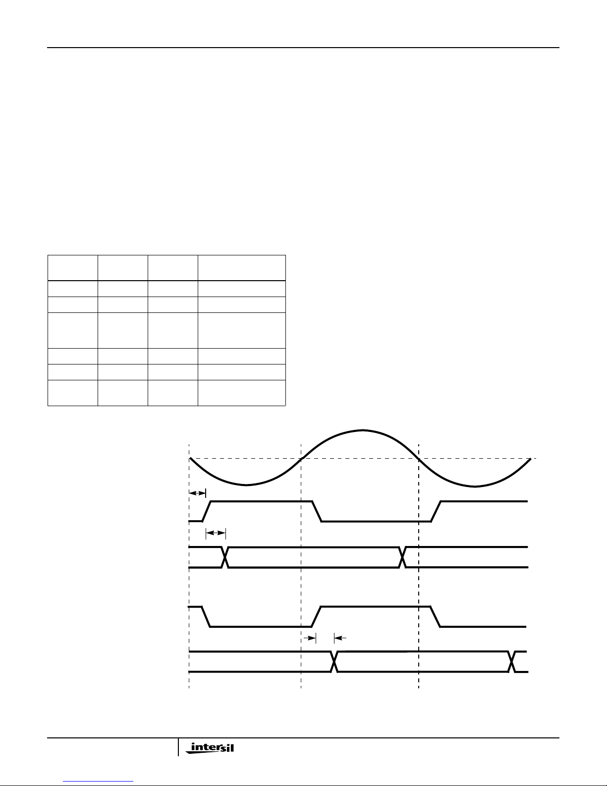
Figure 3 shows the sample clock and digital data timing
relationship for the evaluation board. The data
corresponding to a particular sample will be available at the
digital data outputs of the HI5905 after the data latency time,
t
, of 4 sample clock cycles plus the HI5905 digital data
LAT
output delay, t
expected fortheindicatedtiming delays.Refer to the HI5905
data sheet for additional timing information.
. Table 2 lists the values that can be
OD
SINEWAVE CLK IN
HI5905 SAMPLE
CLOCK INPUT
(CLK AT TP2)
HI5905 DIGITAL
DATA OUTPUT
(CLK AT TP1, P2-C20 OR P2-31)
DIGITAL DATA OUTPUTS
(J2)
(D0 - D13)
CLOCK OUT
(74ALS574)
FIGURE 3. EVALUATION BOARD CLOCK AND DATA TIMING RELATIONSHIPS
t
PD1
t
OD
DATA N-1
DATA N
t
PD2
DATA NDATA N-1
3-3
Page 4
Application Note 9785
TABLE 2. TIMING SPECIFICATIONS
PARAMETER DESCRIPTION TYP
t
t
PD1
t
PD2
OD
HI5905 Digital Output Data Delay 50ns
U4 Prop Delay 4.5ns
U2/3 Prop Delay 9ns
The sample clock and digital output data signals are made
available through two connectors contained on the
evaluation board. The line buffering provided by the data
output latches allows for driving long leads or analyzer
inputs. These data latches are not necessary for the digital
output data if the load presented to the converter does not
exceedthedatasheetloadlimits of 100µA and 15pF. TheP2
I/O connector allows the evaluation board to be interfaced to
the DSP evaluation boards available from Intersil.
Alternatively, the digital output data and sample clock can
also be accessed by clipping the test leads of a logic
analyzer or data acquisition system onto the I/O pins of
connector header P1.
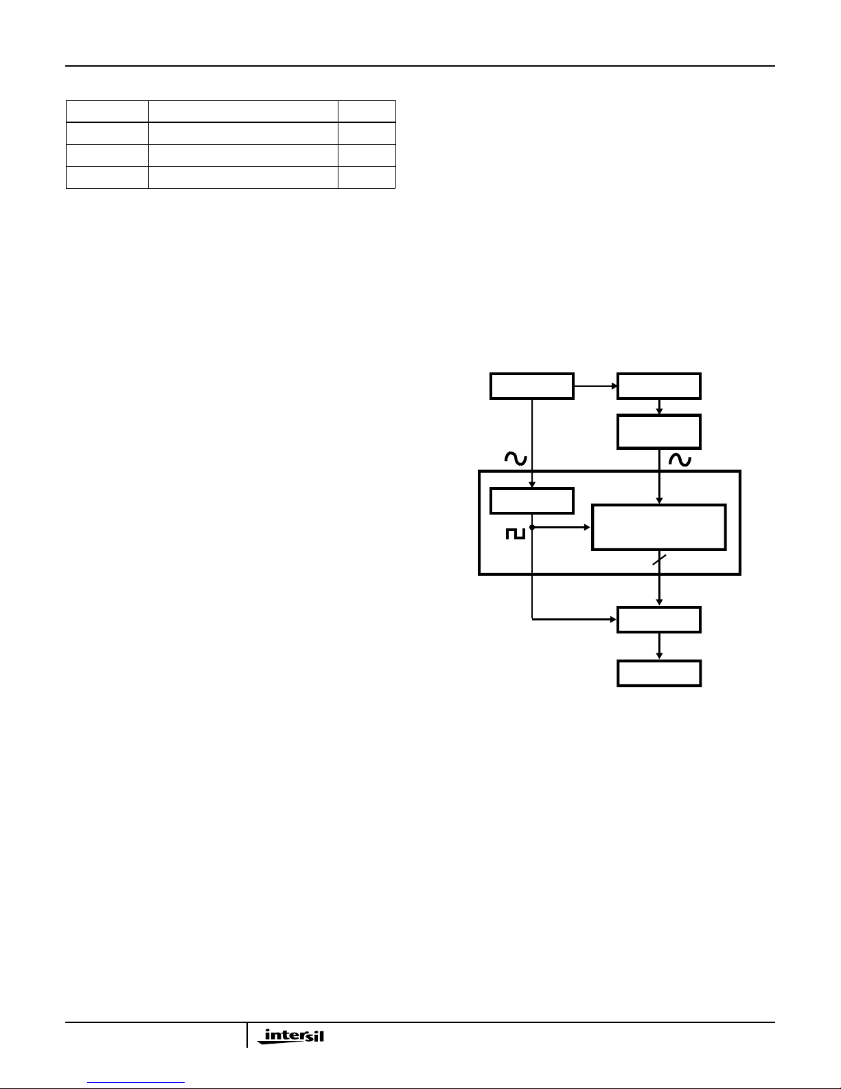
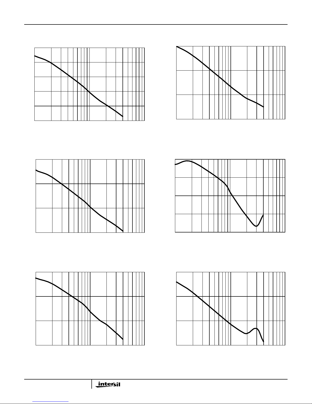
HI5905 Performance Characterization
Dynamic testing is used to evaluate the performance of the
HI5905 A/D converter. Among the tests performed are
Signal-to-Noise and Distortion Ratio (SINAD), Signal-toNoise Ratio (SNR), Total Harmonic Distortion (THD),
Spurious Free Dynamic Range (SFDR) and InterModulation
Distortion (IMD).
Figure 4 shows the test system used to perform dynamic
testing on high-speed ADCs at Intersil. The clock (CLK) and
analog input (V
HP8662A synthesized signal generators that are phase locked
to each other to ensure coherence. The output of the signal
generator driving the ADC analog input is bandpass filtered to
improve the harmonic distortion of the analog input signal. The
comparator on the evaluation board will con v ert the sine wav e
CLK input signal to a square wave at TTL logic le vels to drive
the sample clock input of the HI5905. The ADC data is
captured bya logic analyzer andthentransferred overtheGPIB
) signals are sourced from low phase noise
IN
bustothePC.The PC has the required software to perform the
Fast F ourier Transform (FFT) and do the data analysis.
Coherent testing is recommended in order to avoid the
inaccuracies of windowing. The sampling frequency and
analog input frequency have the following relationship: F
I/FS
= M/N, where FI is the frequency of the input analog
sinusoid, F
is the sampling frequency, N is the number of
S
samples, and M is the number of cycles over which the
samples are taken. By making M an integer and odd number
(1, 3, 5, ...) the samples are assured of being nonrepetitive.
Refer to the HI5905 data sheet for a complete list of test
definitions and the results that can be expected using the
evaluation board with the test setup shown. Evaluating the
part with a reconstruction DAC is only suggested when
doing bandwidth or video testing.
HP8662A
CLK
COMPARATOR
EVALUATION BOARD
FIGURE 4. HIGH-SPEED A/D PERFORMANCE TEST SYSTEM
REF
HI5905EVAL2
HP8662A
BANDPASS
FILTER
V
IN
V
IN
CLK
HI5905
DIGITAL DATA OUTPUT
14
DAS9200
GPIB
PC
3-4
Page 5
Application Note 9785
HI5905EVAL2 Typical Performance (Input Amplitude at -0.5dBFS)
12
11
10
9
ENOB (BITS)
8
7
1
INPUT FREQUENCY (MHz)
10
FIGURE 5. EFFECTIVE NUMBER OF BITS(ENOB) vs INPUT
FREQUENCY
75
65
100
75
65
-THD (dB)
55
45
1
INPUT FREQUENCY (MHz)
10
FIGURE 6. TOTAL HARMONIC DISTORTION(THD) vs INPUT
FREQUENCY
90
80
100
SINAD (dB)
55
45
1
75
65
SNR (dB)
55
70
-2HD (dB)
60
INPUT FREQUENCY (MHz)
10
100
50
1
INPUT FREQUENCY (MHz)
10
FIGURE 7. SINAD vs INPUT FREQUENCY FIGURE 8. SECOND HARMONIC DISTORTION (2HD)vs
INPUT FREQUENCY
80
70
-3HD (BITS)
60
100
45
1
INPUT FREQUENCY (MHz)
10
FIGURE 9. SNR vs INPUT FREQUENCY FIGURE10. THIRD HARMONIC DISTORTION (3HD) vsINPUT
3-5
100
50
1
INPUT FREQUENCY (MHz)
10
100
FREQUENCY
Page 6

Appendix A Board Layout
Application Note 9785
FIGURE 11. HI5905EVAL2 EVALUATION BOARD PARTS LAYOUT (NEAR SIDE)
FIGURE 12. HI5905EVAL2 EVALUATION BOARD COMPONENT NEAR SIDE (LAYER 1)
3-6
Page 7

Appendix A Board Layout (Continued)
Application Note 9785
FIGURE 13. HI5905EVAL2 EVALUATION BOARD GROUND PLANE LAYER (LAYER 2)
FIGURE 14. HI5905EVAL2 EVALUATION BOARD POWER PLANE LAYER (LAYER 3)
3-7
Page 8

Appendix A Board Layout (Continued)
Application Note 9785
FIGURE 15. HI5905EVAL2 EVALUATION BOARD COMPONENT FAR SIDE (LAYER 4)
FIGURE 16. HI5905EVAL2 EVALUATION BOARD PARTS LAYOUT (FAR SIDE)
3-8
Page 9

3-9
Appendix B Schematic Diagrams
V
CC
+
CLK
V
IN+
V
DC
V
IN-
+5V
A
+5V
D1
R4
C10
C9
C7
C6
V
CC
OE
D7
D6
D5
D4
D3
D2
D1
D0
GND
CP
Q7
Q6
Q5
Q4
Q3
Q2
Q1
Q0
‘ALS574
1
2
3
4
5
6
7
8
9
10 11
12
13
14
17
18
19
20
15
16
V
CC
OE
D7
D6
D5
D4
D3
D2
D1
D0
GND
CP
Q7
Q6
Q5
Q4
Q3
Q2
Q1
Q0
‘ALS574
1
2
3
4
5
6
7
8
9
10 11
12
13
14
17
18
19
20
15
16
JP1
U2
U3
R6
R5
D10
D9
D8
D7
D5
D4
D3
D2
D1
D0
D11
D12
D0 - D13,
CLK
+5V
D
+5V
D2
4.7µF
0.1µF
0.1µF
0.1µF
0
+
4.7µF
C18
C17 C14
0.1µF 0.1µF
P1
FB6
4.99K
4.99K
+
4.7µF
C16
C15
0.1µF
+
4.7µF
C12 C11
0.1µF
V
IN-
V
DC
V
IN+
171819
20
24
25
26
HI5905
NC
NC
NC
D6
DV
CC2
D
GND2
D8
D9
NC
D
GND1
U1
2
3
4
5
6
7
8
9
10
11
12
13
14
15
16
21
22
23
27
28
29
30
31
32
331
AV
CC
A
GND
NC
NC
NC
D7
D5
D4
D3
NC
34
35
36
37
38
39
40
41
42
43
44
D2
NC
DV
CC1
D
GND1
DV
CC1
CLK
NC
D0
NC
D1
NC
V
ROUT
D10
D11
D12
D13
A
GND
V
RIN
AV
CC
NC
NC
C13
0.1µF
ALS04
U7
1
2
D6
D13
ALS04
U7
3
4
D13
CLK
CLK
CLK
Application Note 9785
Page 10

Application Note 9785
Appendix B Schematic Diagrams (Continued)
1
7
NC
3
+
-
2
0.1µF
1
NC
2
-
+
3
8
V+
V+
V-
V-
5
4
R15
22.1
R17
499
7
8
V+
V+
V-
V-
5
4
ANALOG
IN
J1
C37
0.1µF
R13
56.2
R18
499
R14
A/R
R20
249
C38
0.1µF
6
U5
OPA628AU
-5V
A
C41C40
4.7µF
+
C43
0.1µF
6
U6
OPA628U
-5V
A
+5V
+
C39
4.7µF
+5V
+
C42
4.7µF
A
C1
0.1µF
VIN+
R16
10
R2
100
R12
0
V
DC
C3
A/R
A
R19
10
C2
0.1µF
R3
100
C5
4.7µF
+
C4
0.1µF
VIN-
+5V
CLK IN
D
J2
R9
249
R8
249
C20
0.1µF
0.1µF
R7
49.9
C25
0.1µF
3(CW)
2
VR1
5K
C44C45
4.7µF
+
+5V
-5V
D
C22
4.7µF
1 (CCW)
C26
0.1µF
D
+
7
8
U4
C24
4.7µF
-5V
TP2
CLK
CLK
TP1
D
C23
0.1µF
1
V+
2
+
-
3
V-
4
+
GND
6
C21
0.1µF
Q
Q
LE
5
MAX9686BCSA
R11
249
R10
249
3-10
Page 11

Application Note 9785
Appendix B Schematic Diagrams (Continued)
P2C
C1
C2
D1 D0
C3
D3
C4
D5
C5
D6
C6
D8
C7
D10
C8
D12
C9
C10
C11
C12
C13
C14
C15
C16
C17
C18
C19
CLK
C20
C21
C22
C23
C24
C25
C26
C27
C28
C29
C30
C31
C32
D2
D4
D7
D9
D11
D13
P2A
A1
A2
A3
A4
A5
A6
A7
A8
A9
A10
A11
A12
A13
A14
A15
A16
A17
A18
A19
A20
A21
A22
A23
A24
A25
A26
A27
A28
A29
A30
A31
A32
D0 - D13,
V
CC
CLK
C8
0.1µF
U7
14
56
7
ALS04
U7
11
ALS04
10
U7
9
ALS04
U7
13
ALS04
8
12
3-11
Page 12

3-12
Appendix B Schematic Diagrams (Continued)
FB1
+
C27
C29
+5VDIN
-5VAIN
+5V
D
-5V
A
FB2
+
C30
C28
+5V
D1
+
+
+
+
+5V
D2
-5V
D
+5VD1IN
+5VD2IN
-5VDIN
+5V
A
+5VAIN
C46
C47
C31 C32
C33 C34
C35
C36
FB3
FB7
FB4
FB5
AGND
DGND
DGND
DGND
DGND
AGND AND DGND TIE TOGETHER
AT A SINGLE POINT WHERE
ENTER THE PWB
THE POWER SUPPLIES
4.7µF
0.1µF
4.7µF
4.7µF
4.7µF
4.7µF
4.7µF
0.1µF
0.1µF
0.1µF
0.1µF
0.1µF
E1 E2
E11 E12
E9 E10
E7 E8
E5 E6
E3 E4
(A/D AV
CC
, OP-AMPS)
(COMPARATOR, D-FF AND INVERTERVIA LPF)
(A/D DV
CC1
)
(A/D DV
CC2
)
(COMPARATOR)
(OP-AMPS)
TP4TP3
+
AGND
Application Note 9785
Page 13

Appendix C Parts List
Application Note 9785
REFERENCE
DESIGNATOR QTY DESCRIPTION
-1Printed Wiring Board
R16, R19 2 10Ω, 1/10W
805 Chip, 1%
R17, R18 2 499Ω, 1/10W
805 Chip, 1%
R13 1 56.2Ω, 1/10W
805 Chip, 1%
R14 1 A/RΩ, 1/10W
805 Chip, 1%
R15 1 22.1Ω, 1/10W
805 Chip, 1%
R2, R3 2 100Ω, 1/10W
805 Chip, 1%
R4, R12 2 0.0Ω, 1/4W
805 Chip, 5%
R5, R6 2 4.99kΩ, 1/10W
805 Chip, 1%
R7 1 49.9Ω, 1/10W
805 Chip, 1%
R8, R9, R10, R11, R20 5 249Ω, 1/10W
805 Chip, 1%
VR1 1 5kΩ Trim Pot
C5, C10, C12, C16, C18,
C22, C24, C27, C29, C31,
C33, C35, C39, C41, C42,
C44, C46
C1, C2, C4, C6, C7, C8,
C9, C11, C13, C14, C15,
C17, C20, C21, C23, C25,
C26, C28, C30, C32, C34,
C36, C37, C38, C40, C43,
C45, C47
C3 1 A/R pF Cer Cap, 50WVDC,
FB1-7 7 10µH Ferrite Bead
J1, J2 2 SMA Straight Jack PCB
- 5 Protective Bumper
JP1 1 1x2 Header
JPH1 1 1x2 Header Jumper
P1 1 2x17 Header
TP1, 2, 3, 4 4 Test Point
U1 1 Intersil HI5905IN, 14-Bit 5
U4 1 Ultrafast Voltage
U2, U3 2 Octal D-type Flip-flop
17 4.7µF Chip Tant Cap,
10WVDC, 20%, EIA Case A
28 0.1µF Cer Cap, 50WVDC,
10%, 805 Case, Y5V
Dielectric
10%, 805 Case
Mount
MSPS A/D Converter
Comparator
REFERENCE
DESIGNATOR QTY DESCRIPTION
U5, U6 2 Op-amp
U7 1 Hex Inverter
P2 64-Pin Eurocard RT Angle
Receptacle
Appendix D HI5905 Theory of Operation
The HI5905 is a 14-bit fully differential sampling pipelined A/D
converter with digital error correction. Figure 17 depicts the
internal circuit for the converters front-end differential-indifferential-outsample-and-hold(S/H).The sampling switches
are controlled byinternalsamplingclocksignals which consist
of two phase non-overlapping clock signals,φ1 and φ2,
derived from the master clock (CLK) driving the converter.
During the sampling phase, φ1, the input signal is applied to
the sampling capacitors, C
capacitors,C
, are dischargedtoanalogground.At the falling
H
edge of φ1 the input analog signal is sampled on the bottom
plates of the sampling capacitors. In the next clock phase, φ2,
the two bottom plates of the sampling capacitors are
connected togetherandtheholding capacitors are switchedto
the op amp output nodes. The charge then redistributes
between C
and CH, completing one sample-and-hold cycle.
S
The output of the sample-and-hold is a fully-differential,
sampled-data representation of the analog input. The circuit
not only performs the sample-and-hold function, but can also
convert a single-ended input to a fully-differential output for
the converter core. During the sampling phase, the V
see only the on-resistance of the switches and C
relatively small values of these components result in a typical
full power input bandwidth of 100MHz for the con verter.
As illustrated in the HI5905 Functional Block Diagram and
the timing diagram contained in Figure 18, three identical
pipeline subconverter stages, each containing a four-bit
flash converter,afour-bit digital-to-analog converter and an
amplifier with a voltage gain of 8, follow the S/H circuit with
the fourth stage being only a 4-bit flash converter. Each
converter stage in the pipeline will be sampling in one
phase and amplifying in the other clock phase. Each
individual sub-converter clock signal is offset by 180
degrees from the previous stage clock signal, with the
result that alternate stages in the pipeline will perform the
same operation. The output of each of the three identical
four-bit subconverter stages is a four-bit digital word
containing a supplementary bit to be used by the digital
error correction logic. The output of each subconverter
stage is input to a digital delay line which is controlled by
the internal clock. The function of the digital delay line is to
time align the digital outputs of the three identical four-bit
subconverter stages with the corresponding output of the
fourth stage flash converter before inputting the sixteen bit
result into the digital error correction logic. The digital error
. At the same time the holding
S
IN
. The
S
pins
3-13
Page 14

Application Note 9785
correction logic uses the supplementary bits to correct any
error that may exist before generating the final fourteen-bit
digital data output (D0-D14) of the converter.
Because of the pipeline nature of this converter, the digital
data representing an analog input sample is presented on
the digital data output bus on the 4th cycle of the clock after
the analog sample is taken. This delay is specified as the
data latency. After the data latency time, the data
representing each succeeding analog sample is output on
the following clock pulse. The output data is synchronized to
the external sampling clock with a data latch and is
presented in offset binary format.
ANALOG
INPUT
VIN+
V
IN
φ
1
φ
1
C
S
φ
2
C
S
φ
1
φ
1
-
+
φ
C
C
1
H
V
OUT
V
OUT
H
φ
1
FIGURE 17. ANALOG INPUT SAMPLE-AND-HOLD
+
-
CLOCK
INPUT
INPUT
S/H
1ST
STAGE
2ND
STAGE
3RD
STAGE
4TH
STAGE
5TH
STAGE
DAT A
OUTPUT
H
N-1
N-1
B
B
2, N-2
4, N-3
S
H
N
B
B
B
1, N-1
3, N-2
5, N-3
D
N-4
N
B
B
2, N-1
4, N-2
S
H
N+1
B
B
B
D
1, N
3, N-1
5, N-2
N-3
N+1
B
B
2, N
4, N-1
t
LAT
S
H
S
N+2
B
1, N+1
B
3, N
B
5, N-1
D
N-2
NOTES:
1. SN: N-th sampling period.
2. HN: N-th holding period.
3. BM,N: M-th stage digital output corresponding to N-th sampled input.
4. DN: Final data output corresponding to N-th sampled input.
FIGURE 18. HI5905 INTERNAL CIRCUIT TIMING
N+2
B
2, N+1
B
4, N
H
N+3
B
1, N+2
B
3, N+1
B
5, N
D
N-1
N+3
B
2, N+2
B
4, N+1
S
H
N+4
B
B
B
D
1, N+3
3, N+2
5, N+1
N
N+4
B
2, N+3
B
4, N+2
S
H
N+5
B
B
B
1, N+4
3, N+3
5, N+2
D
N+1
N+5
B
B
2, N+4
4, N+3
S
H
N+6
B
1, N+5
B
B
D
N+6
3, N+4
5, N+3
N+2
S
3-14
Page 15

HI5905 Functional Block Diagram
Application Note 9785
V
DC
V
IN-
V
IN+
S/H
+
-
∑
X8
+
-
∑
BIAS
4-BIT
FLASH
4-BIT
FLASH
STAGE 1
STAGE 4
4-BIT
DAC
4-BIT
DAC
CLOCK
REF
DIGITAL DELAY
AND
DIGITAL ERROR CORRECTION
CLK
V
ROUT
V
RIN
DV
CC2
D13 (MSB)
D12
D11
D10
D9
D8
D7
D6
D5
D4
D3
D2
X8
FLASH
AV
CCAGNDDVCC1DGND1
3-15
4-BIT
STAGE 5
D1
D0 (LSB)
D
GND2
Page 16

Appendix E Pin Descriptions
Application Note 9785
PIN # NAME DESCRIPTION
1 NC No Connection
2 NC No Connection
3D
GND1
Digital Ground
4 NC No Connection
5AVCCAnalog Supply (5.0V)
6A
GND
Analog Ground
7 NC No Connection
8 NC No Connection
9V
+ Positive Analog Input
IN
10 VIN- Negative Analog Input
11 V
DC
DC Bias Voltage Output
12 NC No Connection
13 V
14 V
15 A
16 AV
ROUT
RIN
GND
CC
Reference Voltage Output
Reference Voltage Input
Analog Ground
Analog Supply (5.0V)
17 NC No Connection
18 D13 Data Bit 13 Output (MSB)
19 D12 Data Bit 12 Output
20 D11 Data Bit 11 Output
21 D10 Data Bit 10 Output
22 NC No Connection
PIN # NAME DESCRIPTION
23 NC No Connection
24 D9 Data Bit 9 Output
25 D8 Data Bit 8 Output
26 D
27 DV
GND2
CC2
Digital Ground
Digital Supply (5.0V)
28 NC No Connection
29 D7 Data Bit 7 Output
30 D6 Data Bit 6 Output
31 D5 Data Bit 5 Output
32 D4 Data Bit 4 Output
33 D3 Data Bit 3 Output
34 NC No Connection
35 NC No Connection
36 D2 Data Bit 2 Output
37 D1 Data Bit 1 Output
38 D0 Data Bit 0 Output (LSB)
39 NC No Connection
40 CLK Input Clock
41 DV
42 D
43 DV
CC1
GND1
CC1
Digital Supply (5.0V)
Digital Ground
Digital Supply (5.0V)
44 NC No Connection
All Intersil semiconductor products are manufactured, assembled and tested under ISO9000 quality systems certification.
Intersil semiconductor products aresold by description only .Intersil Corporation reserves the right to make changesin circuit design and/or specifications at an ytime without notice. Accordingly, the reader is cautioned to verify that data sheets are current bef ore placingorders. Information furnished by Intersil is believed to be accurate and
reliable. Howe ver, no responsibility isassumed by Intersil or its subsidiaries for its use; norfor any infringements of patents or other rights of third parties which mayresult
from its use. No license is granted by implication or otherwise under any patent or patent rights of Intersil or its subsidiaries.
For inf ormationregarding Intersil Corporation and itsproducts, see website www.intersil.com
3-16
 Loading...