Intersil Corporation HI5905 Datasheet

HI5905
Data Sheet January 1999 File Number 4259.3
14-Bit, 5 MSPS A/D Converter
The HI5905 is a monolithic, 14-bit, 5 MSPS Analog-toDigital Converter fabricated in an advanced BiCMOS
process. It is designed for high speed, high resolution
applications where wide bandwidth, low power
consumption and excellent SINAD performance are
essential. With a 100MHz full power input bandwidth and
high frequency accuracy, the converter is ideal for many
types of communication systems employing digital IF
architectures.
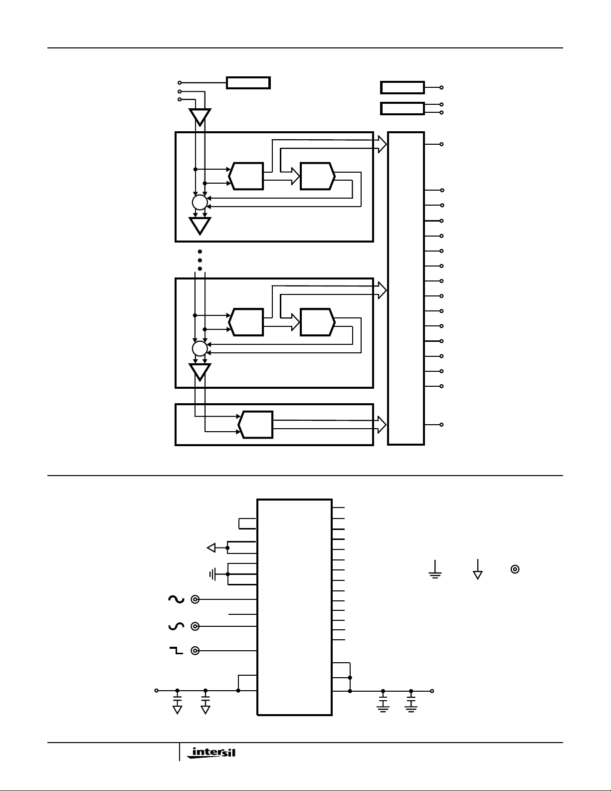
The HI5905 is designed in a fully differential pipelined
architecture with a front end differential-in-differential-out
sample-and-hold amplifier (S/H). The HI5905 has excellent
dynamic performance while consuming 350mW power at 5
MSPS.
Data output latches areprovided which present valid data to
the output bus with a low data latency of 4 clock cycles.
Ordering Information
PART
NUMBER
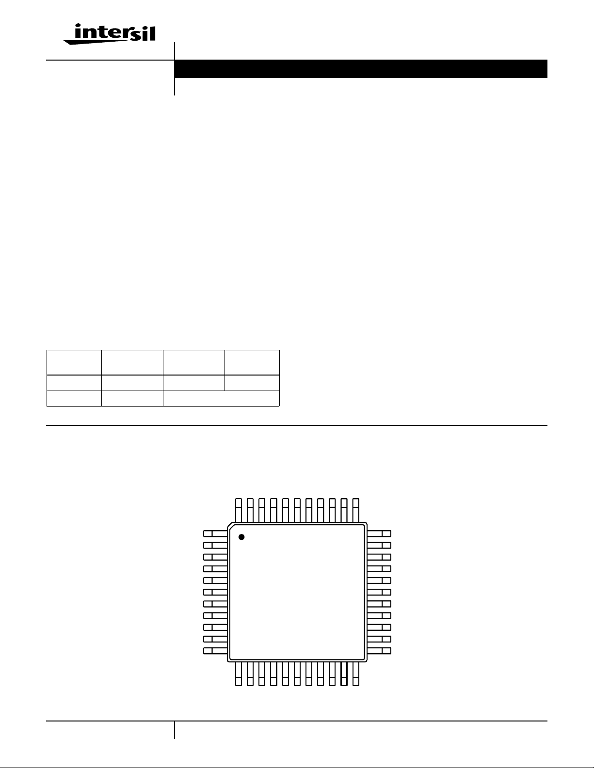
HI5905IN -40 to 85 44 Ld MQFP Q44.10x10
HI5905EVAL2 25 Low Frequency Eval Platform
TEMP. RANGE
(oC) PACKAGE
PKG.
NO.
Features
• Sampling Rate . . . . . . . . . . . . . . . . . . . . . . . . . . . 5 MSPS
• Low Power at 5 MSPS . . . . . . . . . . . . . . . . . . . . . .350mW
• Internal Sample and Hold
• Fully Differential Architecture
• Full Power Input Bandwidth . . . . . . . . . . . . . . . . . 100MHz
• SINAD at 1MHz . . . . . . . . . . . . . . . . . . . . . . . . . . . >70dB
• Low Data Latency
• Internal Voltage Reference
• TTL Compatible Clock Input
• CMOS Compatible Digital Data Outputs
Applications
• Digital Communication Systems
• Undersampling Digital IF
• Asymmetric Digital Subscriber Line (ADSL)
• Document Scanners
• Reference Literature
- AN9214, Using Intersil High Speed A/D Converters
- AN9785, Using the Intersil HI5905 EVAL2 Evaluation
Board
Pinout
D
AV
A
NC
NC
GND1
NC
CC
GND
NC
NC
V
IN+
V
IN-
V
DC
HI5905 (MQFP)
TOP VIEW
CC1
CC1
GND1
D
DV
ROUT
V
V
RIN
DV
GND
A
NC
44 43 42 41 40
1
2
3
4
5
6
7
8
9
10
11
12 13 14 15 16 17
NC
CLKNCD0D1D2NCNC
39 38 37 36 35 34
CC
NC
D13
AV
D12
D11
2221201918
D10
33
32
31
30
29
28
27
26
25
24
23
NC
D3
D4
D5
D6
D7
NC
DV
D
D8
D9
NC
CC2
GND2
13
CAUTION: These devices are sensitive to electrostatic discharge; follow proper IC Handling Procedures.
1-888-INTERSIL or 321-724-7143
| Copyright © Intersil Corporation 1999

Functional Block Diagram
HI5905
V
DC
V
IN
VIN+
-
S/H
+
∑
X8
+
∑
X8
BIAS
STAGE 1
4-BIT
FLASH
4-BIT
DAC
-
STAGE 4
4-BIT
FLASH
4-BIT
DAC
-
STAGE 5
CLOCK
REF
AND
DIGITAL DELAY
DIGITAL ERROR CORRECTION
CLK
V
ROUT
V
RIN
DV
CC2
D13 (MSB)
D12
D11
D10
D9
D8
D7
D6
D5
D4
D3
D2
D1
D0 (LSB)
Typical Application Schematic
+
V
IN
VIN-
CLOCK
+5V
+
10µF
4-BIT
FLASH
AV
CCAGNDDVCC1DGND1
(LSB) D0 (38)
(13)
V
ROUT
V
(14)
RIN
A
(6)
GND
A
(15)
GND
D
(3)
GND1
(42)
D
GND1
D
(26)
GND2
VIN+ (9)
VDC (11)
V
- (10)
IN
(MSB) D13 (18)
CLK (40)
DV
AVCC (5)
AV
0.1µF
CC
(16)
DV
DV
D1 (37)
D2 (36)
D3 (33)
D4 (32)
D5 (31)
D6 (30)
D7 (29)
D8 (25)
D9 (24)
D10 (21)
D11 (20)
D12 (19)
(41)
CC1
(43)
CC1
(27)
CC2
D0
D1
D2
D3
D4
D5
D6
D7
D8
D9
D10
D11
D12
D13
0.1µF
D
GND2
D
GND
10µF AND 0.1µF CAPS ARE PLACED
AS CLOSE TO PART AS POSSIBLE
+5V
+
10µF
A
GND
BNC
14
HI5905

HI5905
Absolute Maximum Ratings Thermal Information
Supply Voltage, AVCC or DVCC to A
D
GND
to A
. . . . . . . . . . . . . . . . . . . . . . . . . . . . . . . . . . . . . .0.3V
GND
Digital I/O Pins . . . . . . . . . . . . . . . . . . . . . . . . . . . . . D
Analog I/O Pins. . . . . . . . . . . . . . . . . . . . . . . . . . . . . .A
Operating Conditions
Temperature Range (HI5905IN) . . . . . . . . . . . . . . . . . -40oC to 85oC
CAUTION: Stresses above those listed in “Absolute Maximum Ratings” may cause permanent damage to the device. This is a stress only rating and operation
of the device at these or any other conditions above those indicated in the operational sections of this specification is not implied.
NOTE:
1. θJA is measured with the component mounted on an evaluation PC board in free air.
GND
or D
. . . . . . . . .+6.0V
GND
GND
GND
to DV
to AV
Thermal Resistance (Typical, Note 1) θJA (oC/W)
MQFP Package. . . . . . . . . . . . . . . . . . . . . . . . . . . . 65
CC
Maximum Junction Temperature (Plastic Package) . . . . . . . .150oC
CC
Maximum Storage Temperature Range . . . . . . . . . .-65oC to 150oC
Maximum Lead Temperature (Soldering 10s) . . . . . . . . . . . . . 300oC
(MQFP - Lead Tips Only)
Electrical Specifications AV
CC
=DV
CC1
=DV
= +5.0V, fS= 5 MSPS at 50% Duty Cycle, V
CC2
RIN=VROUT,CL
= 15pF,
TA = 25oC, Differential Analog Input, Unless Otherwise Specified
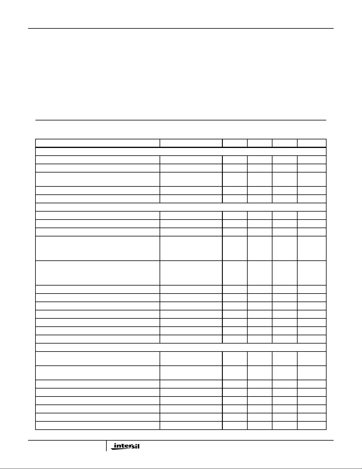
PARAMETER TEST CONDITIONS MIN TYP MAX UNITS
ACCURACY
Resolution 14 - - Bits
Integral Linearity Error, INL Sinewave Histogram - ±2.5 - LSB
Differential Linearity Error, DNL
Sinewave Histogram -1 ±0.5 +1.5 LSB
(Guaranteed No Missing Codes)
Offset Error, V
OS
fIN = DC - - 120 LSB
Full Scale Error, FSE fIN = DC - - 164 LSB
DYNAMIC CHARACTERISTICS
Minimum Conversion Rate No Missing Codes (Note 2) - - 0.5 MSPS
Maximum Conversion Rate No Missing Codes 5 - - MSPS
Effective Number of Bits, ENOB fIN = 1MHz 11.2 11.7 - Bits
Signal to Noise and Distortion Ratio, SINAD fIN = 1MHz 69 72.2 - dB
RMS Signal
--------------------------------------------------------------
=
RMS Noise + Distortion
Signal to Noise Ratio, SNR fIN = 1MHz 71 74.6 - dB
RMS Signal
-------------------------------
=
RMS Noise
Total Harmonic Distortion, THD fIN = 1MHz -73 75.7 - dBc
2nd Harmonic Distortion fIN = 1MHz - -95 dBc
3rd Harmonic Distortion fIN = 1MHz - -77 - dBc
Spurious Free Dynamic Range, SFDR fIN = 1MHz 80 - - dBc
Intermodulation Distortion, IMD f1 = 1MHz, f2 = 1.02MHz - 74 - dBc
Transient Response - 1 - Cycle
Over-Voltage Recovery 0.2V Overdrive - 2 - Cycle
ANALOG INPUT
Maximum Peak-to-P eak Diff erential Analog Input Range
- ±2.0 - V
(VIN+ - VIN-)
Maximum Peak-to-Peak Single-Ended Analog Input
- 4.0 - V
Range
Analog Input Resistance, R
Analog Input Capacitance, C
IN
IN
(Notes 1, 2) 1 - - MΩ
(Note 2) - 10 16 pF
Analog Input Bias Current, IB+ or IB- (Note 3) -50 - +50 µA
Differential Analog Input Bias Current I
= (IB+ - IB-) - ±0.5 - µA
B DIFF
Full Power Input Bandwidth (FPBW) - 100 - MHz
Analog Input Common Mode Voltage Range (VIN+ + VIN-)/2 Differential Mode (Note 2) 1 2.3 4 V
15

HI5905
Electrical Specifications AV
CC
=DV
CC1
=DV
= +5.0V, fS= 5 MSPS at 50% Duty Cycle, V
CC2
RIN=VROUT,CL
= 15pF,
TA = 25oC, Differential Analog Input, Unless Otherwise Specified (Continued)
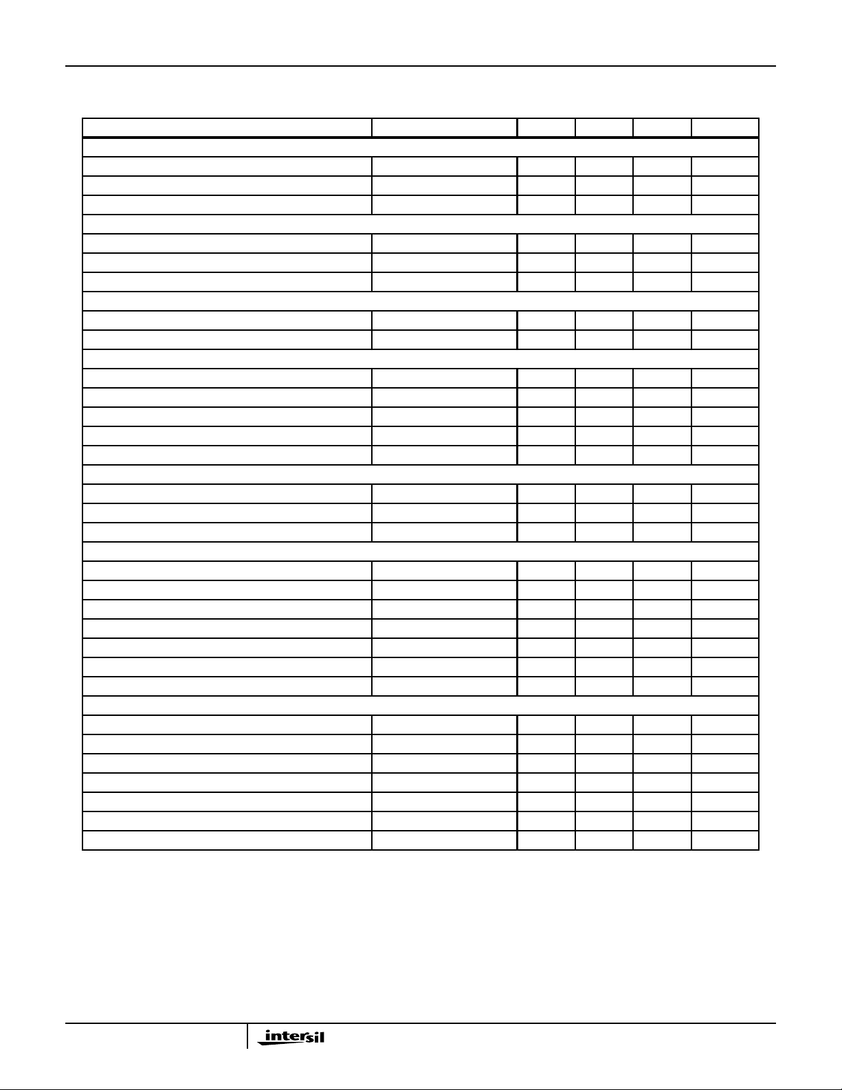
PARAMETER TEST CONDITIONS MIN TYP MAX UNITS
INTERNAL VOLTAGE REFERENCE
Reference Output Voltage, V
ROUT
3.95 4.0 4.05 V
Reference Output Current - - 0.75 mA
Reference Temperature Coefficient - 125 - ppm/oC
REFERENCE VOLTAGE INPUT
Reference Voltage Input, V
RIN
Total Reference Resistance, R
L
- 4.0 - V
- 5.6 - kΩ
Reference Current - 715 - µA
DC BIAS VOLTAGE
DC Bias Voltage Output, V
DC
- 2.3 - V
Max Output Current (Not To Exceed) - - 1 mA
DIGITAL INPUTS (CLK)
Input Logic High Voltage, V
Input Logic Low Voltage, V
Input Logic High Current, I
Input Logic Low Current, I
Input Capacitance, C
IN
IH
IL
V
IH
IL
= 5V -10.0 - +10.0 µA
CLK
V
= 0V -10.0 - +10.0 µA
CLK
2.0 - - V
- - 0.8 V
-10- pF
DIGITAL OUTPUTS (D0-D13)
Output Logic High Voltage, V
Output Logic Low Voltage, V
Output Capacitance, C
OUT
OH
OL
IOH = 100µA 3.5 - - V
IOL = 100µA - - 1.5 V
-5-pF
TIMING CHARACTERISTICS
Aperture Delay, t
Aperture Jitter, t
AP
AJ
Data Output Delay, t
Data Output Hold, t
Data Latency, t
LAT
OD
H
(Note 2) 5 8 - ns
ForaValidSample(Note 2) - - 4 Cycles
-7-ns
- 1 - ps (RMS)
-5060ns
Clock Pulse Width (Low) 5MSPS Clock (Note 2) 95 100 105 ns
Clock Pulse Width (High) 5MSPS Clock (Note 2) 95 100 105 ns
POWER SUPPLY CHARACTERISTICS
Total Supply Current, I
Analog Supply Current, AI
Digital Supply Current, DI
Output Supply Current, DI
CC
CC
CC1
CC2
Power Dissipation VIN+ = VIN- = V
Offset Error PSRR, ∆V
OS
VIN+ = VIN- = V
VIN+ = VIN- = V
VIN+ = VIN- = V
VIN+ = VIN- = V
DC
DC
DC
DC
DC
-7080mA
-50- mA
-14- mA
-6-mA
- 350 400 mW
AVCCor DVCC = 5V ± 5% - 2 - LSB
Gain Error PSRR, ∆FSE AVCC or DVCC = 5V ± 5% - 45 - LSB
NOTES:
2. Parameter guaranteed by design or characterization and not production tested.
3. With the clock off (clock low, hold mode).
16
 Loading...