Intersil Corporation HI5804 Datasheet

Semiconductor
HI5804
See HI5805
NOT RECOMMENDED FOR NEW DESIGNS
October 1998
Features
• Sampling Rate . . . . . . . . . . . . . . . . . . . . . . . . . . 5 MSPS
• Low Power
• Internal Sample and Hold
• Fully Differential Architecture
• Full Power Input Bandwidth . . . . . . . . . . . . . . . 100MHz
[ /Title (HI5804)
• Low Distortion
/Subject (12-Bit, 5 MSPS A/D Converter)
• Internal Reference
/Author ()
• TTL/CMOS Compatible Digital I/O
/Keywords (Harris Semiconductor, A/D, Analog to Digital Converter, Narrow Band, Communications, High
• Digital Outputs. . . . . . . . . . . . . . . . . . . . . . . . . . 3V to 5V
Speed Converters, High Resolution Converters, Basesta-
Applications
tion, Cellular)
/Creator ()
• High Speed Data Acquisition Systems
/DOCINFO pdfmark
• Digital IF Communication Systems
• Document and Film Scanners
[ /PageMode /UseOutlines
• Medical Imaging
/DOCVIEW pdfmark
• Radar Signal Analysis
• Vibration/Waveform Spectrum Analysis
12-Bit, 5 MSPS A/D Converter
Description
The HI5804 is a monolithic, 12-bit, Analog-to-Digital
Converter fabricated in Harris’ HBC10 BiCMOS process. It is
designed for high speed, high resolution applications where
wide bandwidth and low power consumption are essential.
The HI5804 is designed in a fully differential pipelined
architecture with a front end differential-in-differential-out
sample-and-hold (S/H). The HI5804 has excellent dynamic
performance while consuming 300mW power at 5 MSPS.
The 100MHz full power input bandwidth is ideal for
communication systems and document scanner
applications. Data output latches are provided which present
valid data to the output bus with a latency of 3 clock cycles.
The digital outputs have a separate supply pin which can be
powered from a 3.0V to 5.0V supply.
Ordering Information
PART
NUMBER
HI5804KCB 5 MSPS 0 to 70 28 Ld SOIC M28.3
HI5804EVAL 25 Evaluation Board
SAMPLE
RATE
TEMP.
RANGE (oC) PACKAGE
PKG.
NO.
• Digital Servo Loop Control
• Reference Literature
- AN9214 Using Harris High Speed Converters
- AN9647 Using the HI5804 Evaluation Board
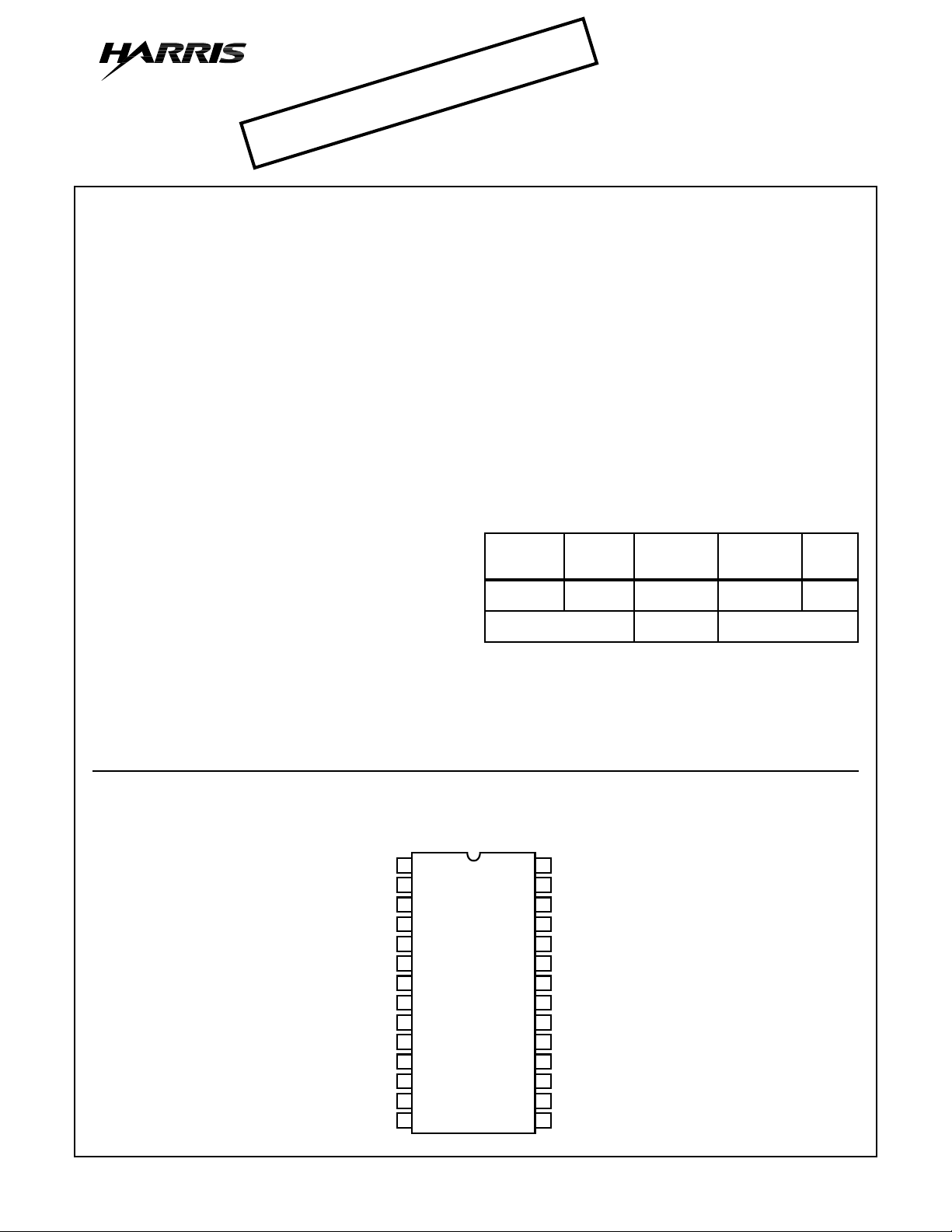
Pinout
CLK
DV
CC1
DGND1
DV
CC1
DGND1
AV
CC
AGND
VIN+
V
V
V
ROUT
V
RIN
AGND
AV
IN
DC
CC
HI5804
(SOIC)
TOP VIEW
1
2
3
4
5
6
7
8
9
10
11
12
13
14
28
27
26
25
24
23
22
21
20
19
18
17
16
15
D0
D1
D2
D3
D4
D5
DV
CC2
DGND2
D6
D7
D8
D9
D10
D11
CAUTION: These devices are sensitive to electrostatic discharge. Users should follow proper IC Handling Procedures.
Copyright
© Harris Corporation 1998
1
File Number 4026.5

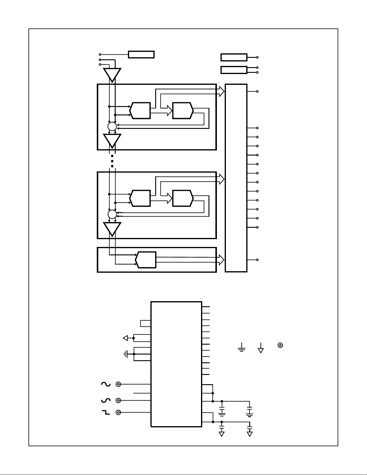
Functional Block Diagram
HI5804
V
DC
V
IN
VIN+
-
BIAS
S/H
STAGE 1
4-BIT
DAC
4-BIT
DAC
X8
X8
4-BIT
FLASH
+
-
∑
STAGE 3
4-BIT
FLASH
+
-
∑
CLOCK
REF
AND
DIGITAL DELAY
DIGITAL ERROR CORRECTION
CLK
V
ROUT
V
RIN
DV
CC2
D11 (MSB)
D10
D9
D8
D7
D6
D5
D4
D3
D2
D1
D0 (LSB)
AV
CC
Typical Application Schematic
+
V
IN
VIN-
CLOCK
STAGE 4
4-BIT
FLASH
AGND DV
V
ROUT
V
RIN
AGND (7)
AGND (13)
DGND1 (3)
DGND1 (5)
DGND2 (21)
VIN+ (8)
VDC(10)
VIN- (9)
CLK (1)
CC1
(LSB) (28) D0
(11)
(12)
(MSB) (15) D11
(22) DV
HI5804
DGND1
(27) D1
(26) D2
(25) D3
(24) D4
(23) D5
(20) D6
(19) D7
(18) D8
(17) D9
(16) D10
(4) DV
(2) DV
(6) AV
(14) AV
CC1
CC1
CC2
CC
CC
D0
D1
D2
D3
D4
D5
D6
D7
D8
D9
D10
D11
0.1µF
0.1µF 10µF
DGND2
DGND AGND
+
10µF
+
BNC
2

HI5804
Absolute Maximum Ratings Thermal Information
Supply Voltage, AVCC or DVCC to A
D
GND
to A
. . . . . . . . . . . . . . . . . . . . . . . . . . . . . . . . . . . . . . .0.3V
GND
Digital I/O Pins . . . . . . . . . . . . . . . . . . . . . . . . . . . . . . D
Analog I/O Pins. . . . . . . . . . . . . . . . . . . . . . . . . . . . . . A
Operating Conditions
Temperature Range, HI5804KCB. . . . . . . . . . . . . . . . . .0oC to 70oC
CAUTION: Stresses above those listed in “Absolute Maxim um Ratings” ma y cause permanent damage to the device . This is a stress only rating and oper ation of
the device at these or any other conditions above those indicated in the operational sections of this specification is not implied.
NOTE:
1. θJA is measured with the component mounted on an evaluation PC board in free air.
GND
or D
. . . . . . . . . . .+6.0V
GND
GND
GND
to DV
to AV
Thermal Resistance (Typical, Note 1) θJA(oC/W)
HI5804KCB . . . . . . . . . . . . . . . . . . . . . . . . . . . . . . . 70
CC
Maximum Junction Temperature. . . . . . . . . . . . . . . . . . . . . . . 150oC
CC
Maximum Storage Temperature Range . . . . . . . . . . -65oC to 150oC
Maximum Lead Temperature (Soldering, 10s) . . . . . . . . . . . . 300oC
(SOIC - Lead Tips Only)
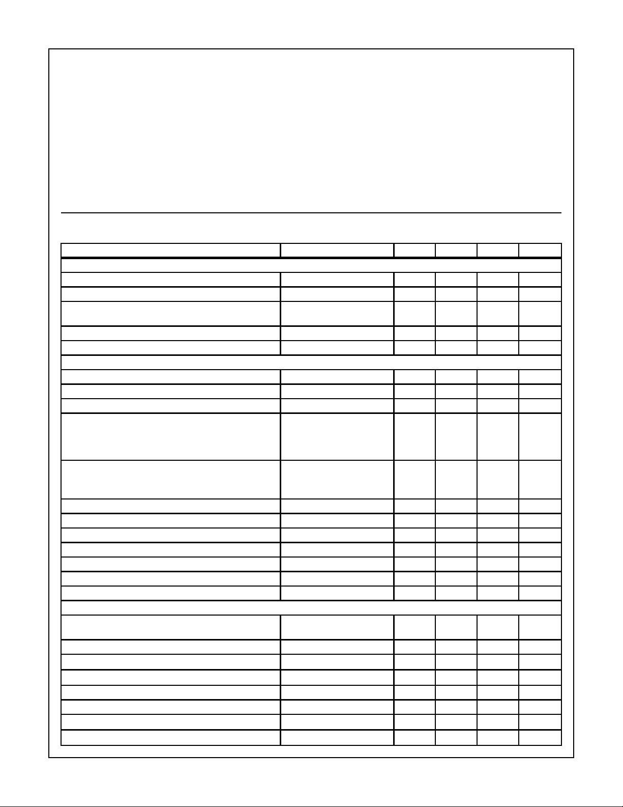
Electrical Specifications AV
CC
= DV
CC1
= DV
= +5.0V, fS = 5 MSPS at 50% Duty Cycle, V
CC2
= 3.5V, CL = 10pF,
RIN
TA = 25oC, Unless Otherwise Specified
PARAMETER TEST CONDITIONS MIN TYP MAX UNITS
ACCURACY
Resolution 12 - - Bits
Integral Linearity Error, INL f
Differential Linearity Error, DNL
= DC - ±2 - LSB
IN
= DC - ±0.5 ±1 LSB
f
IN
(Guaranteed No Missing Codes)
Offset Error, V
OS
Full Scale Error, FSE f
fIN = DC - 12 - LSB
= DC - 24 - LSB
IN
DYNAMIC CHARACTERISTICS
Minimum Conversion Rate No Missing Codes - 0.5 - MSPS
Maximum Conversion Rate No Missing Codes - 5 - MSPS
Effective Number of Bits, ENOB f
Signal to Noise and Distortion Ratio, SINAD f
RMS Signal
--------------------------------------------------------------
=
RMS Noise + Distortion
Signal to Noise Ratio, SNR f
RMS Signal
-------------------------------
=
RMS Noise
= 1MHz - 10.3 - Bits
IN
= 1MHz - 64 - dB
IN
= 1MHz - 65 - dB
IN
Total Harmonic Distortion, THD fIN = 1MHz - -70 - dBc
2nd Harmonic Distortion f
3rd Harmonic Distortion f
Spurious Free Dynamic Range, SFDR f
Intermodulation Distortion, IMD f
= 1MHz - -73 dBc
IN
= 1MHz - -73 - dBc
IN
= 1MHz - 73 - dBc
IN
= 1MHz, f2 = 1.02MHz - -66 - dBc
1
Transient Response - 1 - Cycle
Over-Voltage Recovery 0.2V Overdrive - 2 - Cycle
ANALOG INPUT
Maximum Peak-to-P eak Diff erential Analog Input Range
+ - VIN-)
(V
IN
- ±2.0 - V
Maximum Peak-to-Peak Single-Ended Analog Input Range - 4.0 - V
Analog Input Resistance, R
Analog Input Capacitance, C
Analog Input Bias Current, I
IN
IN
+ or IB- -10 - +10 µA
B
Differential Analog Input Bias Current I
= (IB+ - IB-) - ±0.5 - µA
B DIFF
(Notes 2, 3) 1 -
-10
Full Power Input Bandwidth, FPBW - 100
Analog Input Common Mode Voltage (V
+ + VIN-)/2 Differential Mode (Note 2) 1 2.3
IN
-
-
-
4
MΩ
pF
MHz
V
3

HI5804
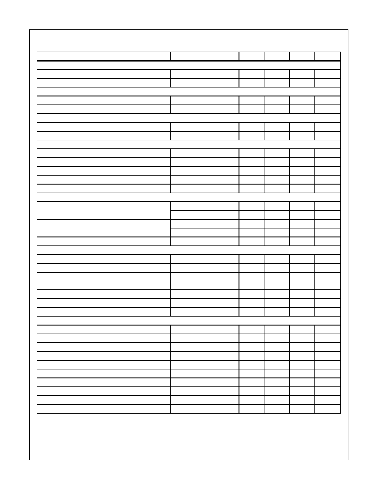
Electrical Specifications AV
CC
= DV
CC1
= DV
= +5.0V, fS = 5 MSPS at 50% Duty Cycle, V
CC2
= 3.5V, CL = 10pF,
RIN
TA = 25oC, Unless Otherwise Specified (Continued)
PARAMETER TEST CONDITIONS MIN TYP MAX UNITS
INTERNAL VOLTAGE REFERENCE
Reference Output Voltage, V
ROUT
- 3.5 - V
Reference Output Current - - 1 mA
REFERENCE INPUT
Total Reference Resistance, R
L
- 7.8 - kΩ
Reference Current - 450 - µA
DC BIAS VOLTAGE
DC Bias Voltage Output, V
DC
- 2.3 - V
Max Output Current (Not to Exceed) - - 1 mA
DIGITAL INPUT, CLK
Input Logic High Voltage, V
Input Logic Low Voltage, V
Input Logic High Current, I
Input Logic Low Current, I
Input Capacitance, C
IN
IH
IL
V
IH
IL
= 5V - - 10.0 µA
CLK
V
= 0V - - 10.0 µA
CLK
2.0 - - V
- - 0.8 V
-7-pF
DIGITAL OUTPUTS, D0-D11
Output Logic Sink Current, I
OL
Output Logic Source Current, I
Output Capacitance, C
OUT
OH
VO = 0.4V (Note 2) 1.6 - - mA
= 3.0V, VO= 0.4V - 1.6 - mA
DV
CC2
VO = 2.4V (Note 2) -0.2 - - mA
= 3.0V, VO = 2.4V - -0.2 - mA
DV
CC2
-5-pF
TIMING CHARACTERISTICS
Aperture Delay, t
Aperture Jitter, t
AP
AJ
Data Output Delay, t
Data Output Hold, t
Data Latency, t
LAT
OD
H
For a Valid Sample (Note 2) - - 3 Cycle
-5-ns
-5-ps
-8-ns
-8-ns
Clock Pulse Width (Low) 5MHz Clock 90 100 110 ns
Clock Pulse width (High) 5MHz Clock 90 100 110 ns
POWER SUPPLY CHARACTERISTICS
Analog Supply Voltage, AV
Digital Supply Voltage, DV
Digital Output Supply Voltage, DV
Total Supply Current, I
Analog Supply Current, AI
Digital Supply Current, DI
Digital Output Supply Current, DI
CC
CC1
CC
CC1
CC
CC2
CC2
VIN+ - VIN- = 2V - 60 - mA
VIN+ - VIN- = 2V - 46 - mA
VIN+ - VIN- = 2V - 13 - mA
VIN+ - VIN- = 2V - 1 - mA
Power Dissipation V
Offset Error Sensitivity, ∆V
OS
AVCCor DVCC = 5V ±5% - ±16 - LSB
Gain Error Sensitivity, ∆FSE AV
+ - VIN- = 2V - 300 - mW
IN
or DVCC = 5V ±5% - ±16 - LSB
CC
4.75 5.0 5.25 V
4.75 5.0 5.25 V
2.85 - 5.25 V
NOTES:
2. Parameter guaranteed by design or characterization and not production tested.
3. With the clock off (clock low, hold mode).
RMS
4
 Loading...