

Intersil Corporation HI5780 Datasheet
August 1997
/
j
/
/
HI5780
10-Bit, 80 MSPS, High Speed,
Low Power D/A Converter
[ /Title
(HI578
0)
Subect
(10Bit, 80
MSPS,
High
Speed,
Low
Power
D/A
Converter)
Autho
r ()
Key-
words
(Intersil
Corporation,
Semiconductor
Communications
Division,
Intersil
Semiconductor,
CommLink,
Features
• Throughput Rate . . . . . . . . . . . . . . . . . . . . . . . 80 MSPS
• Low Power . . . . . . . . . . . . . . . . . . . . . . . . . . . . . .150mW
• Differential Linearity Error . . . . . . . . . . . . . . . ±0.5 LSB
• TTL/CMOS Compatible Inputs
• Built in Bandgap Voltage Reference
• Power Down and Blanking Control Pins
• Direct Replacement for Sony CXD2306
Applications
• Wireless Communications
• Direct Digital Frequency Synthesis
• Signal Reconstruction
• Test Equipment
• High Resolution Imaging and Graphics Systems
• Arbitrary Waveform Generators
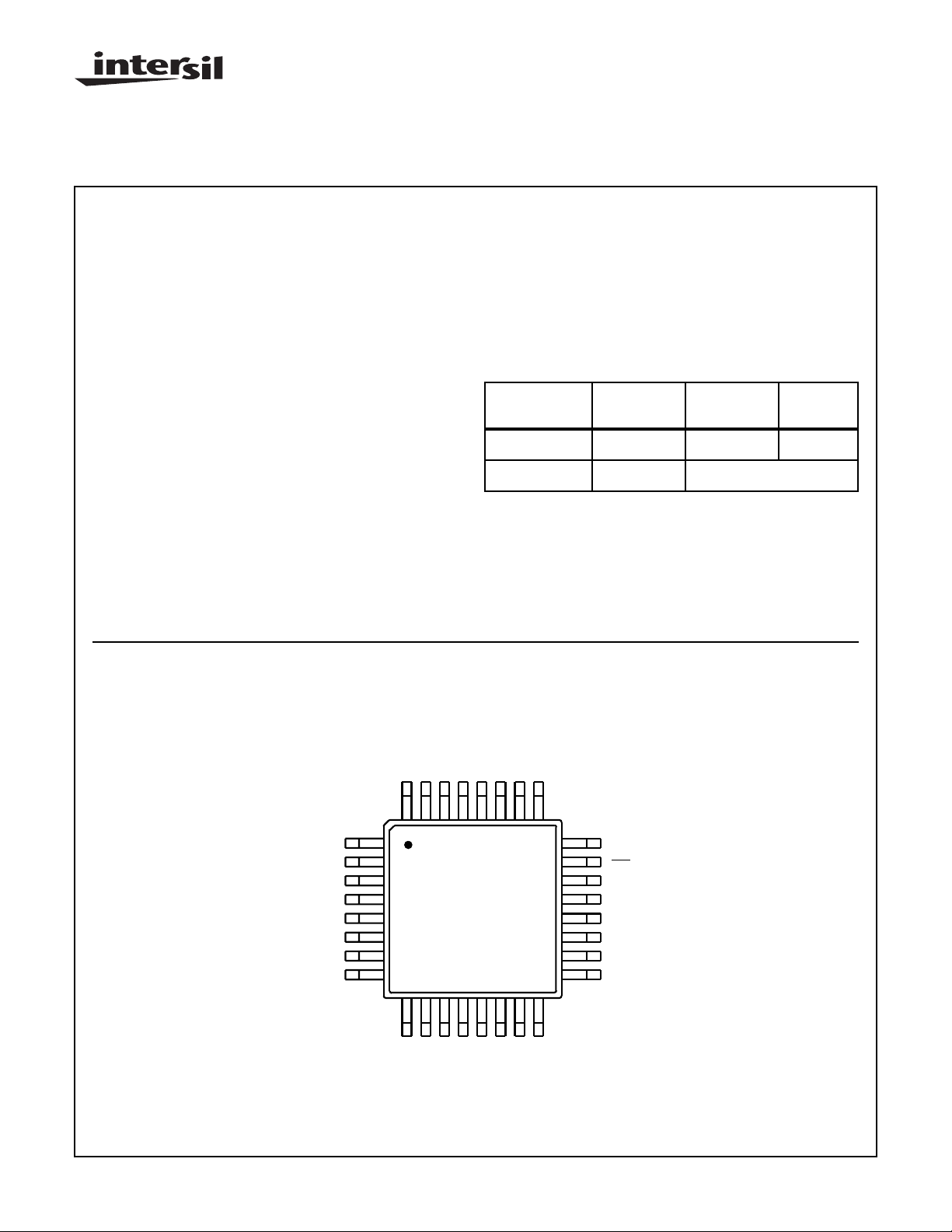
Pinout
(MQFP)
D2D1D0 (LSB)NCDVDDDGNDNCAGND
D3
D4
D5
D6
D7
D8
D9 (MSB)
NC
32 31 30 29 28 27 26 25
1
2
3
4
5
6
7
8
9 10111213141516
PD
CLK
BLK
Description
The HI5780 is a 10-bit, 80 MSPS, high speed, low power
CMOS D/A converter. The converter incorporates a 10-bit input
data register with current outputs. The HI5780 includes a power
down feature that reduces power consumption and a blanking
control. The on-chip bandgap reference can be used to set the
output current range of the D/A.
Ordering Information
PART
NUMBER
HI5780JCQ -20 to 75 32 Ld MQFP Q32.7x7-S
HI5780-EV 25 Evaluation Kit
HI5780
24
23
22
21
20
19
18
17
DD
VB
NC
DV
NC
DGND
TEMP.
RANGE (oC) PACKAGE PKG. NO.
I
OUT
I
OUT
VG
AV
DD
AV
DD
V
REF
REF
OUT
I
REF
CAUTION: These devices are sensitive to electrostatic discharge; follow proper IC Handling Procedures.
http://www.intersil.com or 407-727-9207
| Copyright © Intersil Corporation 1999
10-1716
File Number
4024.4
Typical Application Circuit
HI5780
POWER DOWN CONTROL
50Ω
0.01µF
D9
D8
D7
D6
D5
D4
D3
D2
D1
D0
+5V
HI5780
DV
(13, 28)
DD
D9 (MSB) (7)
D8 (6)
D7 (5)
D6 (4)
D5 (3)
D4 (2)
D3 (1)
D2 (32)
D1 (31)
D0 (30)
CLK (9)
BLK (10)
DGND (8, 12,15, 16,
PD (11)
(20, 21) AV
(18) REF
26, 27, 29)
(22) VG
OUT
(19) V
REF
(14) VB
(24) I
OUT
(23) I
OUT
(17) I
REF
(25) AGND
+5V
0.01µF
DD
0.1µF
0.1µF
D/A OUT
200Ω
2.0kΩ
Functional Block Diagram
(LSB) D0
D1
D2
D3
D4
D5
D6
D7
D8
(MSB) D9
BLK
CLK
VB
PD
DECODER
DECODER
CLOCK
GENERATOR
DAT A
REGISTER
4 LSB
CURRENT
CELLS
6 MSB
CURRENT
CELLS
CURRENT CELLS
(FOR FULL SCALE)
BIAS VOLTAGE
GENERATOR
-
+
BANDGAP
VOLTAGE
REFERENCE
I
OUT
I
OUT
VG
V
REF
I
REF
REF
OUT
10-1717

HI5780
Absolute Maximum Ratings Thermal Information
Supply Voltage VDD to DGND . . . . . . . . . . . . . . . . . . . . . . . . .+7.0V
Digital Input Voltages (D9-D0, CLK, BLANK, PD) . . . . VDD to -0.5V
Internal Reference Output Current. . . . . . . . . . . . . . . . . . . . ±2.5mA
Reference Input Voltage Range (V
Analog Output Current (I
). . . . . . . . . . . . . . . . . . . . . . . . . .15mA
OUT
) . . . . . . . . . . . .VDD to -0.5 V
REF
Operating Conditions
Temperature Range, HI5780BIx. . . . . . . . . . . . . . . . . -20oC to 75oC
CAUTION: Stresses above those listed in “Absolute Maximum Ratings” may cause permanent damage to the device. This is a stress only rating and operation
of the device at these or any other conditions above those indicated in the operational sections of this specification is not implied.
NOTE:
1. θJA is measured with the component mounted on an evaluation PC board in free air.
Thermal Resistance (Typical, Note 1) θJA (oC/W)
MQFP Package. . . . . . . . . . . . . . . . . . . . . . . . . . . . 122
Maximum Junction Temperature (Plastic Package)
Maximum Storage Temperature Range . . . . . . . . . . -65oC to 150oC
Maximum Lead Temperature (Soldering 10s). . . . . . . . . . . . . 300oC
(MQFP - Lead Tips Only)
Electrical Specifications AV
, DVDD = 5.00V, V
DD
REF
= 2.0V, f
= 80 MSPS, R
CLK
LOAD
= 200Ω, R
REF
= 3.3kΩ,
TA = 25oC
HI5780JCQ
PARAMETER TEST CONDITIONS
UNITSMIN TYP MAX
SYSTEM PERFORMANCE
Resolution 10 - - Bits
Integral Linearity Error, INL (Notes 4, 5) (“Best Fit” Straight Line) -2.0 1.25 2.0 LSB
Differential Linearity Error, DNL (Notes 4, 5) -0.5 0.25 0.5 LSB
Offset Error, I
OS
Full Scale Output Current, I
Full Scale Drift Coefficient, I
FS
DRIFT
(Notes 4, 5) - - 5 µA
(Note 4) 9.0 9.6 10 mA
(Note 2) - 0.26 - mV/oC
Output Voltage Compliance Range (Note 3), 10-Bit Accuracy 1.8 1.92 2.0 V
DYNAMIC CHARACTERISTICS
Throughput Rate (Note 3) 80.0 - - MSPS
Output Voltage Full Scale Step
Settling Time, t
SETT FS
Singlet Glitch Area, GE (Peak) R
To ±0.5 LSB Error Band RL = 75Ω, 10-Bit Accuracy
(Note 3)
LOAD
= 75Ω,V
OUT
= 1.0V
(Note 3) - 40 - pV-s
P-P
- 6.0 - ns
Differential Gain, DG (Note 4) - 2.5 - %
Differential Phase, DP (Note 4) - 1.3 - Degrees
Spurious Free Dynamic Range,
SFDR to Nyquist
f
= 40 MSPS, f
CLK
(Note 3)
f
= 80 MSPS, f
CLK
= 2.02MHz, 20MHz Span
OUT
= 2.02MHz, 40MHz Span
OUT
- 48.5 - dBc
- 47.5 - dBc
(Note 3)
f
Spurious Free Dynamic Range, SFDR Within
a Window
= 40 MSPS, f
CLK
f
= 80 MSPS, f
CLK
f
= 40 MSPS, f
CLK
f
= 80 MSPS, f
CLK
f
= 40 MSPS, f
CLK
f
= 80 MSPS, f
CLK
= 10MHz, 20MHz Span (Note 3) - 40.75 - dBc
OUT
= 20MHz, 40MHz Span (Note 3) - 38.5 - dBc
OUT
= 2.02MHz, 2MHz Span (Note 3) - 75.0 - dBc
OUT
= 2.02MHz, 2MHz Span (Note 3) - 73.5 - dBc
OUT
= 10MHz, 2MHz Span (Note 3) - 56.5 - dBc
OUT
= 20MHz, 2MHz Span (Note 3) - 49.0 - dBc
OUT
REFERENCE
Internal Reference Voltage, REF
OUT
(Notes 4, 5) 1.0 1.25 1.3 V
Internal Reference Voltage Drift (Note 3) - 0.34 - mV/oC
Reference Input Voltage Range, V
REF
(Note 3) 0.5 - 2.0 V
10-1718
 Loading...