

Intersil Corporation HI5728 Datasheet
HI5728
Data Sheet July 1999
10-Bit, 125/60MSPS, Dual High Speed
CMOS D/A Converter
The HI5728 is a 10-bit, dual 125MSPS D/A converter which
is implemented in an advanced CMOS process. It is
designed for high speed applications where integration,
bandwidth and accuracy are essential. Operating from a
single +5V or +3V supply, the converter provides20.48mAof
full scale output current and includes an input data register.
Low glitch energy and excellent frequency domain
performance are achieved using a segmented architecture.
A 60MSPS version and an 8-bit (HI5628) version are also
available. Comparable single DAC solutions are the HI5760
(10-bit) and the HI5660 (8-bit). This DACis a member of the
CommLink™ family of communication devices.
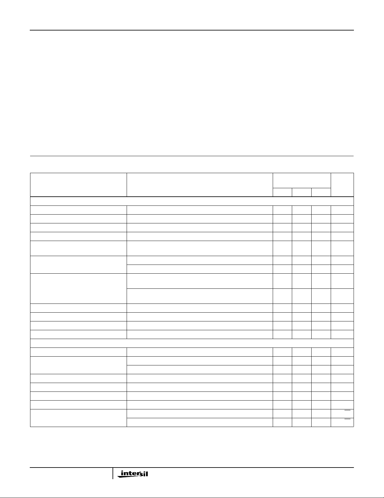
Ordering Information
TEMP.
PART
NUMBER
RANGE
(oC) PACKAGE PKG. NO.
HI5728IN -40 to 85 48 Ld LQFP Q48.7x7A 125MHz
HI5728/6IN -40 to 85 48 Ld LQFP Q48.7x7A 60MHz
HI5728EVAL1 25 Evaluation Platform 125MHz
MAX
CLOCK
SPEED
File Number 4321.4
Features
• Throughput Rate . . . . . . . . . . . . . . . . . . . . . . . .125MSPS
• Low Power . . . . . . . . . . . . . . . 330mW at 5V, 54mW at 3V
• Integral Linearity Error . . . . . . . . . . . . . . . . . . . . . ±1 LSB
• Differential Linearity . . . . . . . . . . . . . . . . . . . . . . ±0.5 LSB
• Gain Matching (Typ). . . . . . . . . . . . . . . . . . . . . . . . . .0.5%
• SFDR at 5MHz Output . . . . . . . . . . . . . . . . . . . . . . .68dBc
• Single Power Supply from +5V to +3V
• CMOS Compatible Inputs
• Excellent Spurious Free Dynamic Range
• Internal Voltage Reference
• Dual 10-Bit D/A Converters on a Monolithic Chip
Applications
• Wireless Local Loop
• Direct Digital Frequency Synthesis
• Wireless Communications
• Signal Reconstruction
• Arbitrary Waveform Generators
• Test Equipment/Instrumentation
• High Resolution Imaging Systems
Pinout
ID6
ID5
ID4
ID3
ID2
ID1
ID0 (LSB)
SLEEP
DV
DD
DGND
NC
AV
DD
ID8
ID7
1
2
3
4
5
6
7
8
9
10
11
12
13 14 15 16
AGND
ICOMP1
TOP VIEW
DD
DV
ID9 (MSB)
DGND
IOUTA
IOUTB
REFLO
HI5728
(LQFP)
ICLK
AGND
QCLK
AGND
QOUTB
DV
DGND
QOUTA
DD
QD9 (MSB)
FSADJ
QD8
QD7
373839404142434445464748
36
35
34
33
32
31
30
29
28
27
26
25
2423222120191817
REFIO
QCOMP1
QD6
QD5
QD4
QD3
QD2
QD1
QD0 (LSB)
DV
DD
DGND
NC
AV
DD
AGND
1
CAUTION: These devices are sensitive to electrostatic discharge; follow proper IC Handling Procedures.
1-888-INTERSIL or 321-724-7143
CommLink™ is a trademark of Intersil Corporation.
| Copyright © Intersil Corporation 1999
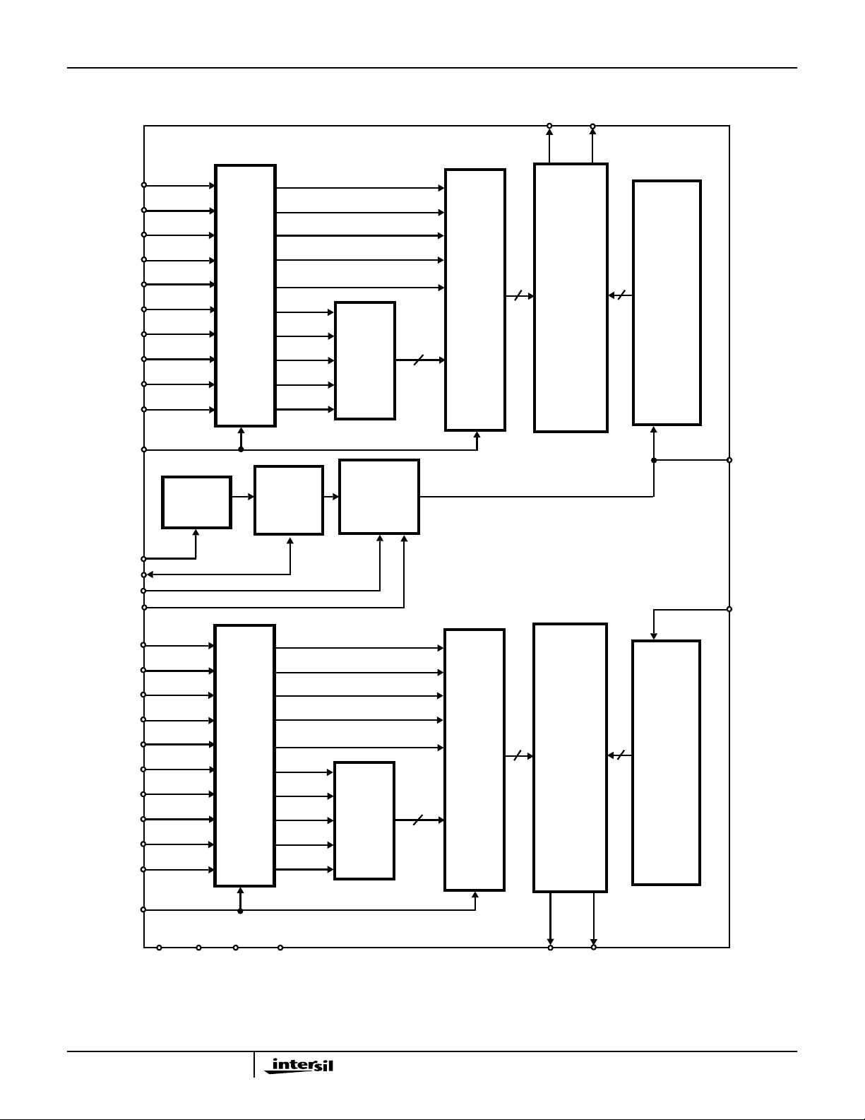
Functional Block Diagram
(LSB) ID0
ID1
ID2
HI5728
IOUTA IOUTB
CASCODE
CURRENT
SOURCE
ID3
ID4
ID5
ID6
ID7
ID8
(MSB) ID9
ICLK
REFLO
REFIO
FSADJ
SLEEP
(LSB) QD0
QD1
QD2
INT/EXT
REFERENCE
SELECT
LATCH
INT/EXT
VOLTAGE
REFERENCE
UPPER
5-BIT
DECODER
BIAS
GENERATION
5 LSBs
36
LATCH
31
SWITCH
MATRIX
36
+
31 MSB
SEGMENTS
CASCODE
CURRENT
SOURCE
ICOMP1
QCOMP1
QD3
QD4
QD5
QD6
QD7
QD8
QCLK
AV
DD
AGND
LATCH
DV
DD
2
DGND
UPPER
5-BIT
DECODER
5 LSBs
36
LATCH
31
SWITCH
MATRIX
QOUTA QOUTB
36
+
31 MSB
SEGMENTS
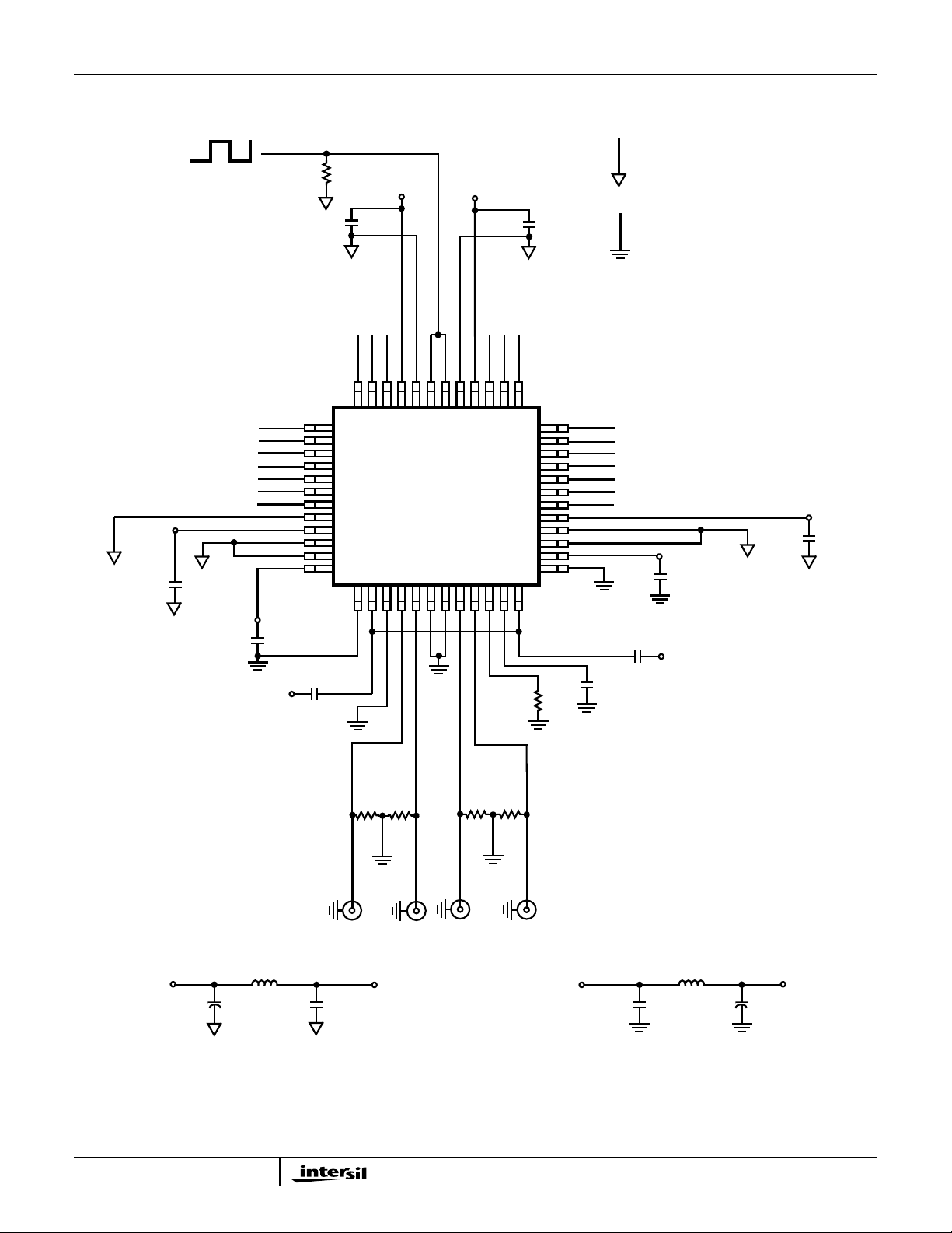
Typical Applications Circuit
50Ω
DV
0.1µF
ID7
DD
ID8
ID9 (MSB)
HI5728
I
CLK/QCLK
DV
DD
0.1µF
QD8
QD7
QD9 (MSB)
DIGITAL
GROUND
PLANE
ANALOG
GROUND
PLANE
SLEEP
DV
DD
0.1µF
ID6
ID5
ID4
ID3
ID2
ID1
ID0 (LSB)
AV
AV
0.1µF
DD
DD
0.1µF
1
2
3
4
5
6
7
8
DV
9
DGND
10
11
NC (GROUND)
12
13 14 15 16
AGND
ICOMP1
DD
50Ω
50Ω
DV
DGND
NC (GROUND)
AGND
AV
50Ω
DD
DD
R
2kΩ
50Ω
373839404142434445464748
2423222120191817
SET
AGND
0.1µF
QD6
QD5
QD4
QD3
QD2
QD1
QD0 (LSB)
AV
DD
0.1µF
AV
0.1µF
DD
NOTE: ICOMP1 AND QCOMP1
PINS (24, 14) MUST BE TIED
TOGETHER EXTERNALLY
0.1µF
DV
DD
36
35
34
33
32
31
30
29
28
27
26
25
QCOMP1
REFIO
+5V OR +3V SUPPLY
+
FERRITE
BEAD
10µH
3
IOUTA
DVDD(POWER PLANE)
0.1µF10µF
IOUTB
QOUTB
QOUTA
(POWER PLANE)
AV
DD
0.1µF
FERRITE
BEAD
10µH
+5V OR +3V SUPPLY
+
10µF
HI5728
Pin Descriptions
PIN NO. PIN NAME PIN DESCRIPTION
39-30 QD9 (MSB) Through
QD0 (LSB)
1-6, 48-46 ID9 (MSB) Through
ID0 (LSB)
8 SLEEP ControlPinfor Power-Downmode. SleepModeis activehigh; Connect toground forNormalMode. Sleep
15 REFLO Connect to analog ground to enable internal 1.2V reference or connect to AVDD to disable.
23 REFIO Reference voltage input if internal reference is disabled and reference voltage output if internal ref erence is
22 FSADJ Full Scale Current Adjust. Use a resistor to ground to adjust full scale output current. Full Scale Output
14, 24 ICOMP1, QCOMP1 Reduces noise. Connect each toAVDDwith 0.1µF capacitorneareachpin. The ICOMP1 and QCOMP1
13, 18, 19, 25 AGND Analog Ground Connections.
17 IOUTB The complimentary current output of the I channel. Bits set to all 0s gives full scale current.
16 IOUTA Current output of the I channel. Bits set to all 1s gives full scale current.
20 QOUTB The complimentary current output of the Q channel. Bits set to all 0s gives full scale current.
21 QOUTA Current output of the Q channel. Bits set to all 1s gives full scale current.
11, 27 NC No Connect. Recommended: connect to ground.
12, 26 AV
10, 28, 41, 44 DGND Digital Ground.
9, 29, 40, 45 DV
43 ICLK Clock input for I channel. Positive edge of clock latches data.
42 QCLK Clock input for Q channel. Positive edge of clock latches data.
DD
DD
Digital Data Bit 9, the Most Significant Bit through Digital Data Bit 0, the Least Significant Bit, of the Q
channel.
Digital DataBit 9, theMost Significant BitthroughDigital DataBit0, the LeastSignificant Bit, oftheI channel.
pin has internal 20µA active pull-down current.
enabled. Use 0.1µF cap to ground when internal reference is enabled.
Current Per Channel = 32 x I
pins MUST be tied together externally.
Analog Supply (+2.7V to +5.5V).
Supply voltage for digital circuitry (+2.7V to +5.5V).
FSADJ
.
4
HI5728
Absolute Maximum Ratings Thermal Information
Digital Supply Voltage DVDD to DCOM . . . . . . . . . . . . . . . . . +5.5V
Analog Supply Voltage AVDD to ACOM. . . . . . . . . . . . . . . . . +5.5V
Grounds, ACOM TO DCOM . . . . . . . . . . . . . . . . . . . -0.3V to +0.3V
Digital Input Voltages (D9-D0, CLK, SLEEP). . . . . . . . .DVDD+0.3V
Internal Reference Output Current. . . . . . . . . . . . . . . . . . . . . ±50µA
Reference Input Voltage Range. . . . . . . . . . . . . . . . . . AVDD+0.3V
Analog Output Current (I
) . . . . . . . . . . . . . . . . . . . . . . . . . 24mA
OUT
Operating Conditions
Temperature Range. . . . . . . . . . . . . . . . . . . . . . . . . . -40oC to 85oC
CAUTION: Stresses above those listed in “Absolute Maximum Ratings” may cause permanent damage to the device. This is a stress only rating and operation of the
device at these or any other conditions above those indicated in the operational sections of this specification is not implied.
NOTE:
1. θJA is measured with the component mounted on an evaluation PC board in free air.
Thermal Resistance (Typical, Note 1) θJA(oC/W)
TQFP Package. . . . . . . . . . . . . . . . . . . . . . . . . . . . . 75
Maximum Power Dissipation
TQFP Package. . . . . . . . . . . . . . . . . . . . . . . . . . . . . . . . . .930mW
Maximum Junction Temperature . . . . . . . . . . . . . . . . . . . . . . .150oC
Maximum Storage Temperature Range. . . . . . . . . . -65oC to 150oC
Maximum Lead Temperature (Soldering 10s) . . . . . . . . . . . . .300oC
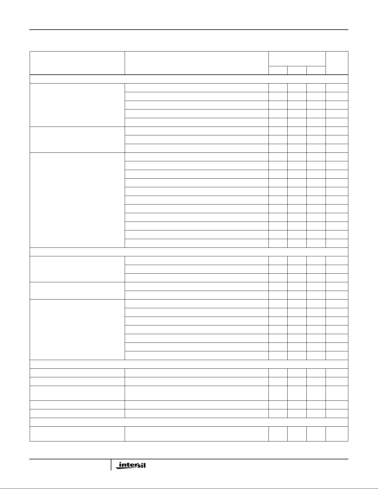
Electrical Specifications AV
PARAMETER TEST CONDITIONS
SYSTEM PERFORMANCE (Per Channel)
Resolution 10 - - Bits
Integral Linearity Error, INL “Best Fit” Straight Line (Note 7) -1 ±0.5 +1 LSB
Differential Linearity Error, DNL (Note 7) -0.5 ±0.25 +0.5 LSB
Offset Error, I
Offset Drift Coefficient (Note 7) - 0.1 - ppm
Full Scale Gain Error, FSE With External Reference (Notes 2, 7) -10 ±2 +10 % FSR
Full Scale Gain Drift With External Reference (Note 7) - ±50 - ppm
Gain Matching Between Channels -0.5 0.1 0.5 dB
I/Q Channel Isolation F
Output Voltage Compliance Range (Note 3) -0.3 - 1.25 V
Full Scale Output Current, I
DYNAMIC CHARACTERISTICS (Per Channel)
Maximum Clock Rate, f
Output Settling Time, (t
Singlet Glitch Area (Peak Glitch) RL = 25Ω (Note 7) - 35 - pV•s
Output Rise Time Full Scale Step - 1.5 - ns
Output Fall Time Full Scale Step - 1.5 - ns
Output Capacitance -10- pF
Output Noise IOUTFS = 20mA - 50 - pA/√Hz
OS
FS
CLK
) 0.1% (±1 LSB, equivalent to 9 Bits) (Note 7) - 20 - ns
SETT
= DVDD = +5V, V
DD
per channel except for ‘Power Supply Characteristics.’
(Note 7) -0.025 +0.025 % FSR
With Internal Reference (Notes 2, 7) -10 ±1 +10 % FSR
With Internal Reference (Note 7) - ±100 - ppm
= 10MHz - 80 - dB
OUT
(Note 3) 125 - - MHz
0.05% (±1/2 LSB, equivalent to 10 Bits) (Note 7) - 35 - ns
IOUTFS = 2mA - 30 - pA/√Hz
= Internal 1.2V, IOUTFS = 20mA, TA = 25oC for All Typical Values. Data given is
REF
HI5728IN
TA = -40oC TO 85oC
UNITSMIN TYP MAX
FSR/oC
FSR/oC
FSR/oC
2 - 20 mA
5
HI5728
Electrical Specifications AV
= DVDD = +5V, V
DD
= Internal 1.2V, IOUTFS = 20mA, TA = 25oC for All Typical Values. Data given is
REF
per channel except for ‘Power Supply Characteristics.’ (Continued)
HI5728IN
TA = -40oC TO 85oC
PARAMETER TEST CONDITIONS
UNITSMIN TYP MAX
AC CHARACTERISTICS (Per Channel) - HI5728IN - 125MHz
Spurious Free Dynamic Range,
SFDR Within a Window
Total Harmonic Distortion (THD) to
Nyquist
Spurious Free Dynamic Range,
SFDR to Nyquist
f
= 125MSPS, f
CLK
f
= 100MSPS, f
CLK
f
= 60MSPS, f
CLK
f
= 50MSPS, f
CLK
f
= 50MSPS, f
CLK
f
= 100MSPS, f
CLK
f
= 50MSPS, f
CLK
f
= 50MSPS, f
CLK
f
= 125MSPS, f
CLK
f
= 125MSPS, f
CLK
f
= 100MSPS, f
CLK
f
= 100MSPS, f
CLK
f
= 100MSPS, f
CLK
f
= 100MSPS, f
CLK
f
= 60MSPS, f
CLK
f
= 50MSPS, f
CLK
f
= 50MSPS, f
CLK
f
= 50MSPS, f
CLK
f
= 50MSPS, f
CLK
= 32.9MHz, 10MHz Span (Notes 4, 7) - 75 - dBc
OUT
= 5.04MHz, 4MHz Span (Notes 4, 7) - 76 - dBc
OUT
= 10.1MHz, 10MHz Span (Notes 4, 7) - 75 - dBc
OUT
= 5.02MHz, 2MHz Span (Notes 4, 7) - 76 - dBc
OUT
= 1.00MHz, 2MHz Span (Notes 4, 7) - 78 - dBc
OUT
= 2.00MHz (Notes 4, 7) - 71 - dBc
OUT
= 2.00MHz (Notes 4, 7) - 71 - dBc
OUT
= 1.00MHz (Notes 4, 7) - 76 - dBc
OUT
= 32.9MHz, 62.5MHz Span (Notes 4, 7) - 54 - dBc
OUT
= 10.1MHz, 62.5MHz Span (Notes 4, 7) - 64 - dBc
OUT
= 40.4MHz, 50MHz Span (Notes 4, 7) - 52 - dBc
OUT
= 20.2MHz, 50MHz Span (Notes 4, 7) - 60 - dBc
OUT
= 5.04MHz, 50MHz Span (Notes 4, 7) - 68 - dBc
OUT
= 2.51MHz, 50MHz Span (Notes 4, 7) - 74 - dBc
OUT
= 10.1MHz, 30MHz Span (Notes 4, 7) - 63 - dBc
OUT
= 20.2MHz, 25MHz Span (Notes 4, 7) - 55 - dBc
OUT
= 5.02MHz, 25MHz Span (Notes 4, 7) - 68 - dBc
OUT
= 2.51MHz, 25MHz Span (Notes 4, 7) - 73 - dBc
OUT
= 1.00MHz, 25MHz Span (Notes 4, 7) - 73 - dBc
OUT
AC CHARACTERISTICS (Per Channel) - HI5728/6IN - 60MHz
Spurious Free Dynamic Range,
SFDR Within a Window
Total Harmonic Distortion (THD) to
Nyquist
Spurious Free Dynamic Range,
SFDR to Nyquist
f
= 60MSPS, f
CLK
f
= 50MSPS, f
CLK
f
= 50MSPS, f
CLK
f
CLK
f
CLK
f
= 60MSPS, f
CLK
f
= 60MSPS, f
CLK
f
= 50MSPS, f
CLK
f
= 50MSPS, f
CLK
f
= 50MSPS, f
CLK
f
= 50MSPS, f
CLK
f
= 25MSPS, f
CLK
= 50MSPS, f
= 50MSPS, f
= 10.1MHz, 10MHz Span (Notes 4, 7) - 75 - dBc
OUT
= 5.02MHz, 2MHz Span (Notes 4, 7) - 76 - dBc
OUT
= 1.00MHz, 2MHz Span (Notes 4, 7) - 78 - dBc
OUT
= 2.00MHz (Notes 4, 7) - 71 - dBc
OUT
= 1.00MHz (Notes 4, 7) - 76 - dBc
OUT
= 20.2MHz, 30MHz Span (Notes 4, 7) - 56 - dBc
OUT
= 10.1MHz, 30MHz Span (Notes 4, 7) - 63 - dBc
OUT
= 20.2MHz, 25MHz Span (Notes 4, 7) - 55 - dBc
OUT
= 5.02MHz, 25MHz Span (Notes 4, 7) - 68 - dBc
OUT
= 2.51MHz, 25MHz Span (Notes 4, 7) - 73 - dBc
OUT
= 1.00MHz, 25MHz Span (Notes 4, 7) - 73 - dBc
OUT
= 5.02MHz, 25MHz Span (Notes 4, 7) - 71 - dBc
OUT
VOLTAGE REFERENCE
Internal Reference Voltage, V
FSADJ
Voltage at Pin 22 with Internal Reference 1.04 1.16 1.28 V
Internal Reference Voltage Drift - ±60 - ppm/oC
Internal Reference Output Current
- 0.1 - µA
Sink/Source Capability
Reference Input Impedance -1-MΩ
Reference Input Multiplying Bandwidth (Note 7) - 1.4 - MHz
DIGITAL INPUTS D9-D0, CLK (Per Channel)
Input Logic High Voltage with
5V Supply, V
IH
(Note 3) 3.5 5 - V
6
 Loading...