Intersil Corporation HI5721 Datasheet
HI5721
Data Sheet June 1999
10-Bit, 125 MSPS, High Speed D/A
Converter
The HI5721 is a 10-bit, 125 MSPS, high speed D/A
converter. The converter incorporates a 10-bit, input data
register with quadrature data logic capability and current
outputs. The HI5721 features low glitch energy and excellent
frequency domain specifications.
Ordering Information
PART
NUMBER
HI5721BIP -40 to 85 28 Ld PDIP E28.6
HI5721BIB -40 to 85 28 Ld SOIC (W) M28.3
HI5721-EVP 25 Evaluation Board (PDIP)
HI5721-EVS 25 Evaluation Board (SOIC)
TEMP.
RANGE (oC) PACKAGE
PKG.
NO.
File Number 3949.7
Features
• Throughput Rate . . . . . . . . . . . . . . . . . . . . . . . 125 MSPS
• Low Power . . . . . . . . . . . . . . . . . . . . . . . . . . . . . . .700mW
• Integral Linearity Error . . . . . . . . . . . . . . . . . . . . . 1.5 LSB
• Low Glitch Energy . . . . . . . . . . . . . . . . . . . . . . . . 1.5pV•s
• TTL/CMOS Compatible Inputs
• Improved Hold Time. . . . . . . . . . . . . . . . . . . . . . . . . 0.5ns
• Excellent Spurious Free Dynamic Range
• Improved Second Source for the AD9721
Applications
• Wireless Communications
• Direct Digital Frequency Synthesis
• Signal Reconstruction
• HDTV
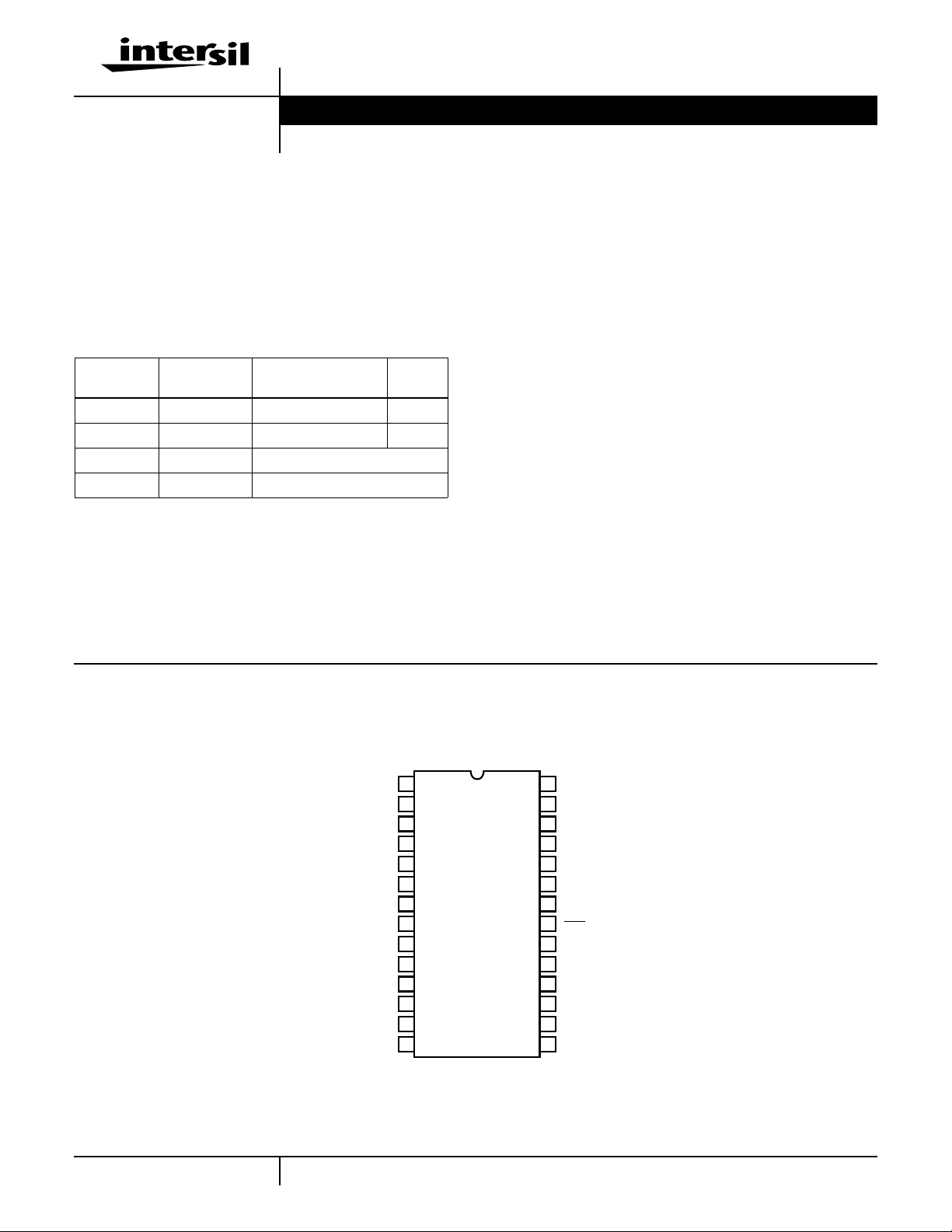
Pinout
D9 (MSB)
D8
D7
D6
D5
D4
D3
D2
D1
D0 (LSB)
CLOCK
NC
INVERT
V
CC
1
2
3
4
5
6
7
8
9
10
11
12
13
14
HI5721
(PDIP, SOIC)
TOP VIEW
• Test Equipment
• High Resolution Imaging Systems
• Arbitrary Waveform Generators
DGND
28
27
DV
EE
26
CTRL AMP IN
25
REF OUT
24
CTRL AMP OUT
23
REF IN
22
AV
EE
21
I
OUT
20
I
OUT
19
ARTN
18
AGND
17
R
SET
16
DV
EE
15
DGND
3-34
CAUTION: These devices are sensitive to electrostatic discharge; follow proper IC Handling Procedures.
1-888-INTERSIL or 321-724-7143
| Copyright © Intersil Corporation 1999
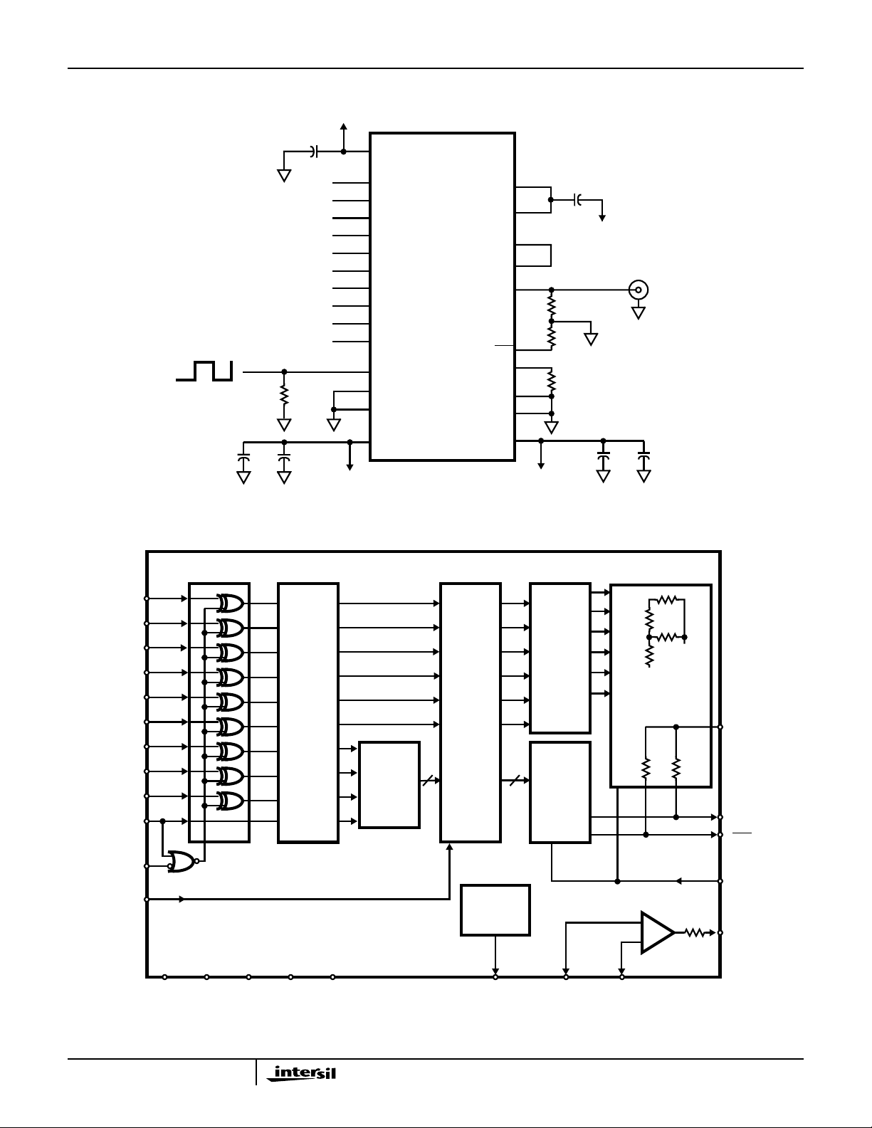
Typical Applications Circuit
0.01µF
+5V
V
CC
HI5721
HI5721
(14)
50Ω
0.1µF
Functional Block Diagram
QUADRATURE
LOGIC
D9
D8
D7
D6
D5
D4
D3
D2
D1
D0
0.01µF
- 5.2V (DVEE)
D9 (MSB) (1)
D8 (2)
(24) CTRL AMP OUT
D7 (3)
D6 (4)
D5 (5)
D4 (6)
D3 (7)
D2 (8)
D1 (9)
D0 (LSB) (10)
CLK (11)
INVERT (13)
DGND (15, 28)
DVEE (16, 27)
(26) CTRL AMP IN
(23) REF IN
(25) REF OUT
(20) I
OUT
(21) I
OUT
(17) R
SET
(19) ARTN
(18) AGND
(22) AV
EE
- 5.2V (AVEE)
0.1µF
-5.2V (AVEE)
64Ω
64Ω
1960Ω
0.01µF
D/A OUT
0.1µF
(LSB) D0
D1
D2
D3
D4
D5
D6
D7
D8
(MSB) D9
INVERT
CLK
DAT A
BUFFER/
LEVEL
SHIFTER
AVEEAGND DVEEDGND V
CC
UPPER
4-BIT
DECODER
15
SLAVE
REGISTER
VOLTAGE
REFERENCE
REF OUT R
15
6 LSBs
CURRENT
CELLS
15
SWITCHED
CURRENT
CELLS
SET
R2R
NETWORK
227Ω 227Ω
+
-
CTRL AMP IN
25Ω
ARTN
I
OUT
I
OUT
REF IN
CTRL AMP
OUT
3-35
HI5721
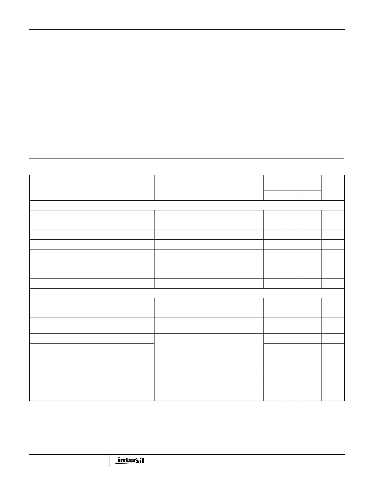
Absolute Maximum Ratings Thermal Information
Digital Supply Voltage VCC to DGND . . . . . . . . . . . . . . . . . . .+5.5V
Negative Digital Supply Voltage DVEE to DGND . . . . . . . . . . -5.5V
Negative Analog Supply Voltage AVEE to AGND, ARTN. . . . . -5.5V
Digital Input Voltages (D9-D0, CLK, INVERT). . . . . . .VCC to -0.5 V
Internal Reference Output Current. . . . . . . . . . . . . . . . . . . . . .500µA
Control Amplifier Input Voltage Range. . . . . . . . . . . .AGND to -4.0V
Control Amplifier Output Current . . . . . . . . . . . . . . . . . . . . . ±2.5mA
Reference Input Voltage Range. . . . . . . . . . . . . . . . . -3.7 V to AV
Analog Output Current (I
) . . . . . . . . . . . . . . . . . . . . . . . . . 30mA
OUT
EE
Operating Conditions
Temperature Range. . . . . . . . . . . . . . . . . . . . . . . . . . -40oC to 85oC
CAUTION: Stresses above those listed in “Absolute Maximum Ratings” may cause permanent damage to the device. This is a stress only rating and operation of the
device at these or any other conditions above those indicated in the operational sections of this specification is not implied.
NOTE:
1. θJA is measured with the component mounted on an evaluation PC board in free air.
Thermal Resistance (Typical, Note 1) θJA(oC/W)
PDIP Package . . . . . . . . . . . . . . . . . . . . . . . . . . . . . 55
SOIC Package . . . . . . . . . . . . . . . . . . . . . . . . . . . . . 70
Maximum Power Dissipation
HI5721BIx . . . . . . . . . . . . . . . . . . . . . . . . . . . . . . . . . . . . .750mW
Maximum Junction Temperature
HI5721BIx . . . . . . . . . . . . . . . . . . . . . . . . . . . . . . . . . . . . . .150oC
Maximum Storage Temperature Range. . . . . . . . . . -65oC to 150oC
Maximum Lead Temperature (Soldering 10s) . . . . . . . . . . . . .300oC
(SOIC - Lead Tips Only)
Electrical Specifications AV
PARAMETER TEST CONDITIONS
SYSTEM PERFORMANCE
Resolution 10 - - Bits
Integral Linearity Error, INL (Note 4) (“Best Fit” Straight Line) - ±0.5 ±1.5 LSB
Differential Linearity Error, DNL (Note 4) - ±0.5 ±1.0 LSB
Offset Error, I
Full Scale Gain Error, FSE (Notes 2, 4) - 2 10 %
Offset Drift Coefficient (Note 3) - 0.1 - µA/oC
Full Scale Output Current, I
Output Voltage Compliance Range (Note 3) -1.5 - +3.0 V
DYNAMIC CHARACTERISTICS
Throughput Rate (Note 3) 125.0 - - MSPS
Output Voltage Full Scale Step Settling Time, t
Output Voltage Small Step Settling Time, t
Singlet Glitch Area, GE (Peak Glitch) RL = 50Ω (Note 3) - 3.5 - pV•s
Doublet Glitch Area, (Net Glitch) - 1.5 - pV•s
Output Slew Rate RL = 50Ω,DAC Operating in Latched Mode
Output Rise Time RL = 50Ω,DAC Operating in Latched Mode
Output Fall Time RL = 50Ω,DAC Operating in Latched Mode
OS
FS
, DVEE = -4.94 to -5.46V, VCC = +4.75 to +5.25V, CTRL AMP IN = REF OUT,
EE
TA = 25oC for All Typical Values
(Note 4) - 16 75 µA
SETT FS
SETT SM
To ±0.5 LSB Error Band RL = 50Ω (Note 3) - 4.5 - ns
100mV Step to ±0.5 LSB Error Band, RL = 50Ω
(Note 3)
(Note 3)
(Note 3)
(Note 3)
HI5721BI
TA = -40oC TO 85oC
UNITSMIN TYP MAX
- -20.48 - mA
- 3.5 - ns
- 1,000 - V/µs
- 675 - ps
- 470 - ps
3-36
HI5721
Electrical Specifications AV
, DVEE = -4.94 to -5.46V, VCC = +4.75 to +5.25V, CTRL AMP IN = REF OUT,
EE
TA = 25oC for All Typical Values (Continued)
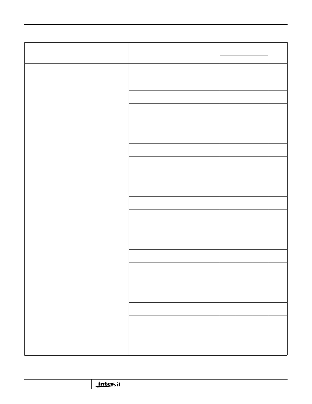
PARAMETER TEST CONDITIONS
Spurious Free Dynamic Range, SFDR to Nyquist f
Spurious Free Dynamic Range, SFDR Within a
Window
Signal to Noise Ratio (SNR) to Nyquist
(Ignoring the First 5 Harmonics)
Signal to Noise Ratio + Distortion (SINAD) to Nyquist f
Total Harmonic Distortion (THD) to Nyquist f
Intermodulation Distortion (IMD) to Nyquist f
= 125 MSPS, f
CLK
Span (Notes 3, 5)
f
=125 MSPS, f
CLK
(Notes 3, 5)
f
=100 MSPS, f
CLK
(Notes 3, 5)
f
= 100 MSPS, f
CLK
(Notes 3, 5)
f
= 125 MSPS, f
CLK
(Notes 3, 5)
f
= 125 MSPS, f
CLK
(Notes 3, 5)
f
= 100 MSPS, f
CLK
(Notes 3, 5)
f
= 100 MSPS, f
CLK
(Notes 3, 5)
f
= 125 MSPS, f
CLK
(Notes 3, 5)
f
= 125 MSPS, f
CLK
(Notes 3, 5)
f
= 100 MSPS, f
CLK
(Notes 3, 5)
f
= 100 MSPS, f
CLK
(Notes 3, 5)
= 125 MSPS, f
CLK
(Notes 3, 5)
f
= 125 MSPS, f
CLK
(Notes 3, 5)
f
= 100 MSPS, f
CLK
(Notes 3, 5)
f
= 100 MSPS, f
CLK
(Notes 3, 5)
= 125 MSPS, f
CLK
(Notes 3, 5)
f
= 125 MSPS, f
CLK
(Notes 3, 5)
f
= 100 MSPS, f
CLK
(Notes 3, 5)
f
= 100 MSPS, f
CLK
(Notes 3, 5)
= 125 MSPS, f
CLK
f
= 900kHz (Notes 3, 5)
OUT2
f
= 100 MSPS, f
CLK
f
= 900kHz (Notes 3, 5)
OUT2
= 2.02MHz, 62.5MHz
OUT
=25MHz, 62.5MHz Span
OUT
=2.02MHz, 50MHz Span
OUT
= 25MHz, 50MHz Span
OUT
= 2.02MHz, 2MHz Span
OUT
= 25MHz, 2MHz Span
OUT
= 2.02MHz, 2MHz Span
OUT
= 25MHz, 2MHz Span
OUT
= 2.02MHz,
OUT
= 25MHz
OUT
= 2.02MHz,
OUT
= 25MHz
OUT
= 2.02MHz,
OUT
= 25MHz
OUT
= 2.02MHz,
OUT
= 25MHz
OUT
= 2.02MHz,
OUT
= 25MHz
OUT
= 2.02MHz,
OUT
= 25MHz
OUT
= 800kHz,
OUT1
= 800kHz,
OUT1
HI5721BI
TA = -40oC TO 85oC
UNITSMIN TYP MAX
- -59 - dBc
- -53 - dBc
- -59 - dBc
- -51 - dBc
- -75 - dBc
- -70 - dBc
- -75 - dBc
- -72 - dBc
-54- dB
- 51.5 - dB
- 54.5 - dB
- 50.3 - dB
- 52.4 - dB
- 49.2 - dB
- 52.7 - dB
- 47.6 - dB
- -57.8 - dBc
- -53.3 - dBc
- -57.9 - dBc
- -51 - dBc
- 57.3 - dB
- 57.2 - dB
3-37
HI5721
Electrical Specifications AV
, DVEE = -4.94 to -5.46V, VCC = +4.75 to +5.25V, CTRL AMP IN = REF OUT,
EE
TA = 25oC for All Typical Values (Continued)
HI5721BI
TA = -40oC TO 85oC
PARAMETER TEST CONDITIONS
UNITSMIN TYP MAX
REFERENCE/CONTROL AMPLIFIER
Internal Reference Voltage, REF OUT (Note 4) -1.15 -1.25 -1.35 V
Internal Reference Voltage Drift (Note 3) - 100 - µV/oC
Internal Reference Output Current Sink/Source
(Note 3) -50 - +500 µA
Capability
Amplifier Input Impedance (Note 3) - 10 - MΩ
Amplifier Large Signal Bandwidth 4.0V
Sine Wave Input, to Slew Rate Limited
P-P
- 1 - MHz
(Note 3)
Amplifier Small Signal Bandwidth 1.0V
Sine Wave Input, to -3dB Loss (Note 3) - 10 - MHz
P-P
Reference Input Impedance (Note 3) - 4.6 - kΩ
Reference Input Multiplying Bandwidth RL = 50Ω, 100mV Sine Wave, to -3dB Loss at
I
(Note 3)
OUT
- 75 - MHz
DIGITAL INPUTS (D9-D0, CLK, INVERT)
Input Logic High Voltage, V
Input Logic Low Voltage, V
Input Logic Current, I
Input Logic Current, I
IH
IL
Digital Input Capacitance, C
IH
IL
IN
(Note 4) 2.0 - - V
(Note 4) - - 0.8 V
(Note 4) - - 400 µA
(Note 4) - - 700 µA
(Note 3) - 3.0 - pF
TIMING CHARACTERISTICS
Data Setup Time, t
Data Hold Time, t
SU
HLD
Propagation Delay Time, t
CLK Pulse Width, t
PW1
, t
PD
PW2
See Figure 3 (Note 3) 2.0 - - ns
See Figure 3 (Note 3) 0.5 - - ns
See Figure 3 (Note 3) - 4.5 - ns
See Figure 3 (Note 3) 1.0 0.85 - ns
POWER SUPPLY CHARACTERISITICS
IDV
IAV
V
EE
EE
CC
(Note 4) - 100 110 mA
(Note 4) - - 15 mA
(Note 4) - 14 25 mA
Power Dissipation (Note 4) - 700 775 mW
Power Supply Rejection Ratio VCC±5%, VEE±5% - 50 - µA/V
NOTES:
2. Gain Error measured as the error in the ratio between the full scale output current and the current through R
(typically 640µA). Ideally the
SET
ratio should be 32.
3. Parameter guaranteed by design or characterization and not production tested.
4. All devices are 100% tested at 25oC. 100% productions tested at temperature extremes for military temperature devices, sample tested for industrial temperature devices.
5. Spectral measurements made without external filtering.
3-38
 Loading...