

Intersil Corporation HI5714 Datasheet

HI5714
January 1998
Features
• Sampling Rate . . . . . . . . . . . . . . . . . .40/60/75/80 MSPS
• Low Power . . . . . . . . . . . . . . . . . . . . . . . . . . . . . .325mW
• 7.65 ENOB at 4.43MHz
• Overflow/Underflow Three-State TTL Output
• Operates with Low Level AC Clock
• Very Low Analog Input Capacitance
• No Buffer Amplifier Required
• No Sample and Hold Required
• TTL Compatible I/O
• Pin-Compatible to Philips TDA8714
Applications
• Video Digitizing
• QAM Demodulator
• Digital Cable Setup Box
• Tape Drive/Mass Storage
• Medical Ultrasound Imaging
• Communication Systems
8-Bit, 40/60/75/80 MSPS A/D Converter
Description
The HI5714 is a high precision, monolithic, 8-bit, Analog-toDigital Converter fabricated in Intersil’ advanced HBC10
BiCMOS process.
The HI5714 is optimized for a wide range of applications such as
ultrasound imaging, mass storage, instrumentation, and video
digitizing, where accuracy and low power consumption are
essential. The HI5714 is offered in 40 MSPS, 60 MSPS, and 75
MSPS sample rates.
The HI5714 delivers ±0.4 LSB differential nonlinearity while
consuming only 325mW power (Typical) at 75 MSPS. The
digital inputs and outputs are TTL compatible, as well as
allowing for a low-level sine wave clock input.
Ordering Information
TEMP.
PART
NUMBER
HI5714/4CB 0 to 70 24 Ld SOIC 40 M24.3
HI5714/6CB 0 to 70 24 Ld SOIC 60 M24.3
HI5714/7CB 0 to 70 24 Ld SOIC 75 M24.3
HI5714/8CB 0 to 70 24 Ld SOIC 80 M24.3
HI5714EVAL 25 Evaluation Board
RANGE
(oC) PACKAGE
SAMPLING
FREQUENCY
(MHz)
PKG.
NO.
Pinout
HI5714
(SOIC)
TOP VIEW
D1
1
D0
2
NC
3
V
4
RB
NC
5
AGND
6
V
7
CCA
8
V
IN
9
V
RT
10
NC
11
O/UF
12
D7
CAUTION: These devices are sensitive to electrostatic discharge; follow proper IC Handling Procedures.
1-888-INTERSIL or 321-724-7143 | Copyright © Intersil Corporation 1999
24
D2
D3
23
OE
22
V
21
CCO2
OGND
20
V
19
CCO1
V
18
CCD
DGND
17
16
CLK
D4
15
D5
14
D6
13
1
File Number 3973.4

Functional Block Diagram
HI5714
V
V
V
OGND
RT
RB
V
CCA
7
CLOCK DRIVER
9
IN
8
4
20
ANALOG TO DIGITAL
CONVERTER
6
AGND DGND
17
OVERFLOW/UNDERFLOW
CLK V
16
LATCHES
LATCH
CCD
18
OE
22
TTL OUTPUTS
TTL OUTPUT
D7
12
D6
13
D5
14
15
D4
D3
23
D2
24
1
D1
2
D0
V
CCO1
19
V
CCO2
21
O/UF
11
Typical Application Schematic
+5VA
BNC
+
-
CLOCK
0.1
1.3V
V
IN
DGND
AGND
3.6V
+
-
+
-
+5VA
0.1
1nF 0.1µF
2
16
CLK
9
V
RT
4
V
RB
22
OE
HI5714
8
V
IN
7
V
CCA
5
NC
6
AGND
D0
D1
D2
D3
D4
D5
D6
D7
O/UF
V
CCO
V
CCO
V
CCD
OGND
NC
DGND
NC
1
24
23
15
14
13
12
11
19
21
18
1nF
0.1µF
20
3
17
10
+5VD
1nF and 0.1µF CAPS are placed
as close to part as possible.
NOTES:
1. Pin 5 should be connected to AGND and pins 3 and 10 to DGND to reduce noise coupling into the device.
2. Analog and Digital supplies should be separated and decoupled to reduce digital noise coupling into the analog supply.
2
HI5714
Absolute Maximum Ratings T
V
CCA,VCCD
V
CCA
V
CCO
V
CCA
VIN,V
I
OUT
, V
. . . . . . . . . . . . . . . . . . . . . . . . . -0.3V to +6.0V
- V
- V
- V
CLK,VRT,VRB
CCO
. . . . . . . . . . . . . . . . . . . . . . . . . . . . . . . . . . . . . . 0.3V
CCD
. . . . . . . . . . . . . . . . . . . . . . . . . . . . . . . . . . . . . . 0.3V
CCD
. . . . . . . . . . . . . . . . . . . . . . . . . . . . . . . . . . . . . . 0.3V
CCO
, OE . . . . . . . . . . . . . . . . . . . . . . -0.3V to +6.0V
, Digital Pins . . . . . . . . . . . . . . . . . . . . . . . . . . . . . . . . . . 10mA
=25oC Thermal Information
A
Thermal Resistance (Typical, Note 1) θJA (oC/W)
SOIC Package. . . . . . . . . . . . . . . . . . . . . . . . . . . . . 75
Maximum Junction Temperature (Plastic Package) . . . . . . . . 150oC
Maximum Storage Temperature Range . . . . . . . . . -65oC to 150oC
Maximum Lead Temperature (Soldering 10s). . . . . . . . . . . . . 300oC
(SOIC - Lead Tips Only)
Input Current, All Pins. . . . . . . . . . . . . . . . . . . . . . . . . . . . . . . . 1mA
Digital I/O Pins . . . . . . . . . . . . . . . . . . . . . . . . . . . . OGND to V
CCO
Operating Conditions
Temperature Range
HI5714CB . . . . . . . . . . . . . . . . . . . . . . . . . . . . . . . . . 0oC to 70oC
CAUTION: Stresses above those listed in “Absolute Maximum Ratings” may cause permanent damage to the device. This is a stress only rating and operation
of the device at these or any other conditions above those indicated in the operational sections of this specification is not implied.
NOTE:
1. θJA is measured with the component mounted on an evaluation PC board in free air.
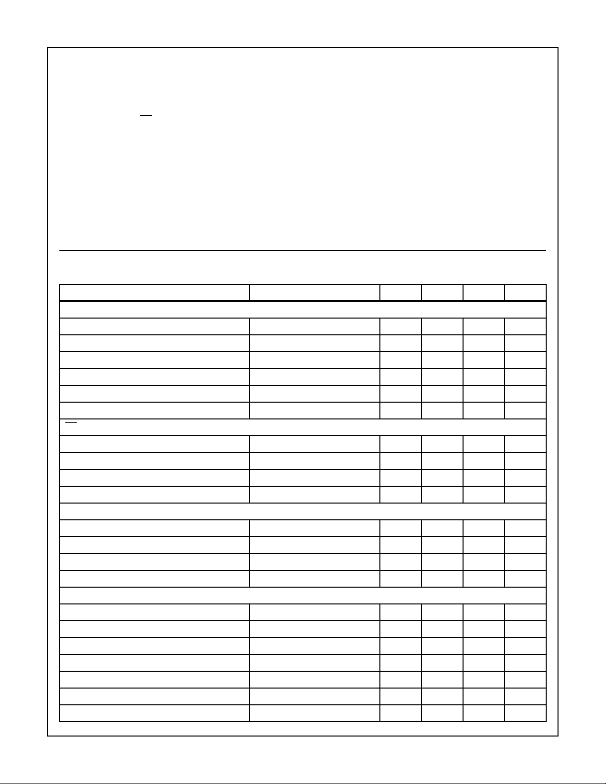
Electrical Specifications V
PARAMETER TEST CONDITION MIN TYP MAX UNITS
CLOCK (Referenced to DGND) (Note 1)
Logic Input Voltage Low, V
Logic Input Voltage High, V
Logic Input Current Low, I
Logic Input Current High, I
Input Impedance, Z
Input Capacitance, C
OE (Referenced to DGND)
Logic Input Voltage Low, V
Logic Input Voltage High, V
Logic Input Current Low, I
Logic Input Current High, I
VIN(Referenced to AGND)
Input Current Low, I
Input Current High, I
Input Impedance, Z
Input Capacitance, C
REFERENCE INPUT
Bottom Reference Range, V
Top Reference Range, V
Reference Range, V
Reference Current, I
Reference Ladder Resistance, R
R
LADTC
Bottom Offset Voltage, V
IL
IN
IN
IL
IL
IH
IN
IN
RT
REF(VRT
REF
OB
IL
IH
IH
IL
IH
IH
RB
- VRB) 1.9 2.3 2.7 V
CCA
= V
CCD
= V
CCO
Unless Otherwise Specified
V
CLK
V
CLK
f
CLK
f
CLK
VIL= 0.4V -400 - - µA
VIH= 2.7V - - 20 µA
VIN= 1.2V - 0 - µA
VIN= 3.5V - 100 180 µA
fIN= 4.43MHz - 10 - kΩ
fIN= 4.43MHz - 14 - pF
LAD
(Note 4) - 255 - mV
= +5V; VRB= 1.3V; VRT= 3.6V; TA =25oC,
0 - 0.8 V
2.0 - V
CCD
= 0.4V -400 - - µA
= 2.7V - - 300 µA
= 75MHz (Note 8) - 2 - kΩ
= 75MHz (Note 8) - 4.5 - pF
0 - 0.8 V
2.0 - V
CCD
1.2 1.3 1.6 V
3.5 3.6 3.9 V
-10-mA
- 240 - Ω
- 0.24 - Ω/oC
V
V
3
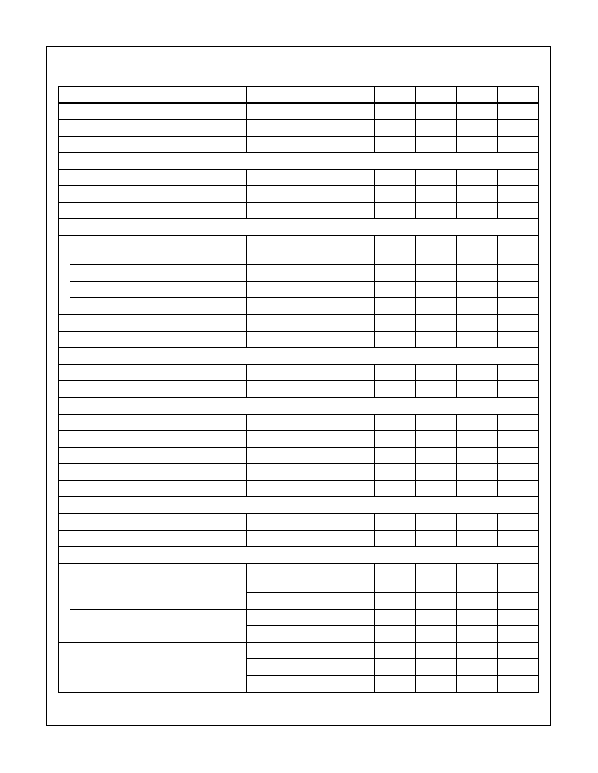
HI5714
Electrical Specifications V
CCA
= V
CCD
= V
= +5V; VRB= 1.3V; VRT= 3.6V; TA =25oC,
CCO
Unless Otherwise Specified (Continued)
PARAMETER TEST CONDITION MIN TYP MAX UNITS
V
OBTC
Top Offset Voltage, V
V
OTTC
OT
(Note 4) - 136 - µV/oC
(Note 4) - -300 - mV
(Note 4) - 480 - µV/oC
DIGITAL OUTPUTS (D0 to D7 and O/UF Referenced to OGND)
Logic Output Voltage Low, V
Logic Output Voltage High, V
Output Leakage Current, I
D
OL
OH
IO = 1mA 0 - 0.4 V
IO = -0.4mA 2.7 - V
0.4V < V
OUT
< V
CCO
-20 - +20 µA
CCO
SWITCHING CHARACTERISTICS (Notes 3, 4) See Figure 9
Sample Rate, f
CLK
HI5714/8 80 - - MHz
HI5714/7 75 - - MHz
HI5714/6 60 - - MHz
HI5714/4 40 - - MHz
Clock Pulse Width High, t
Clock Pulse Width Low, t
CPH
CPL
ANALOG SIGNAL PROCESSING (f
CLK
= 40MHz)
6--ns
6--ns
Differential Gain, DG (Notes 5, 8) - 1.0 - %
Differential Phase, DP (Notes 5, 8) - 0.05 - degree
HARMONICS (f
CLK
= 75MHz)
Second Harmonic, H2 fIN= 4.43MHz - -63 - dB
Third Harmonic, H3 fIN= 4.43MHz - -65 - dB
Total Harmonic Distortion, THD fIN= 4.43MHz - -59 - dB
Spurious Free Dynamic Range, SFDR fIN= 4.43MHz - 62 - dB
Analog Input Bandwidth (-3dB) - 18 - MHz
TRANSFER FUNCTION
Differential Linearity Error, DNL (Note 6) - ±0.4 - LSB
Integral Linearity Error, INL (Note 6) - ±0.75 - LSB
EFFECTIVE NUMBER OF BITS
ENOB
HI5714/4 (f
= 40MHz) fIN= 4.43MHz - 7.65 - Bits
CLK
fIN= 7.5MHz - 7.5 - Bits
HI5714/6 (f
= 60MHz) fIN= 4.43MHz - 7.65 - Bits
CLK
fIN= 7.5MHz - 7.5 - Bits
HI5714/7 (f
= 75MHz) fIN= 4.43MHz - 7.4 - Bits
CLK
fIN= 7.5MHz - 7.15 - Bits
fIN= 10MHz - 6.8 - Bits
V
4
 Loading...