Intersil Corporation HI-5701-883 Datasheet

HI-5701/883
June 1994
Features
• This Circuit is Processed in Accordance to MIL-STD883 and is Fully Conformant Under the Provisions of
Paragraph 1.2.1.
• 30 MSPS with No Missing Codes
• 20MHz Full Power Input Bandwidth
• No Missing Codes Over Temperature
• Sample and Hold Not Required
• Single +5V Supply Voltage
• CMOS/TTL
• Overflow Bit
Applications
• Video Digitizing
• Radar Systems
• Medical Imaging
• Communication Systems
6-Bit, 30 MSPS Flash A/D Converter
Description
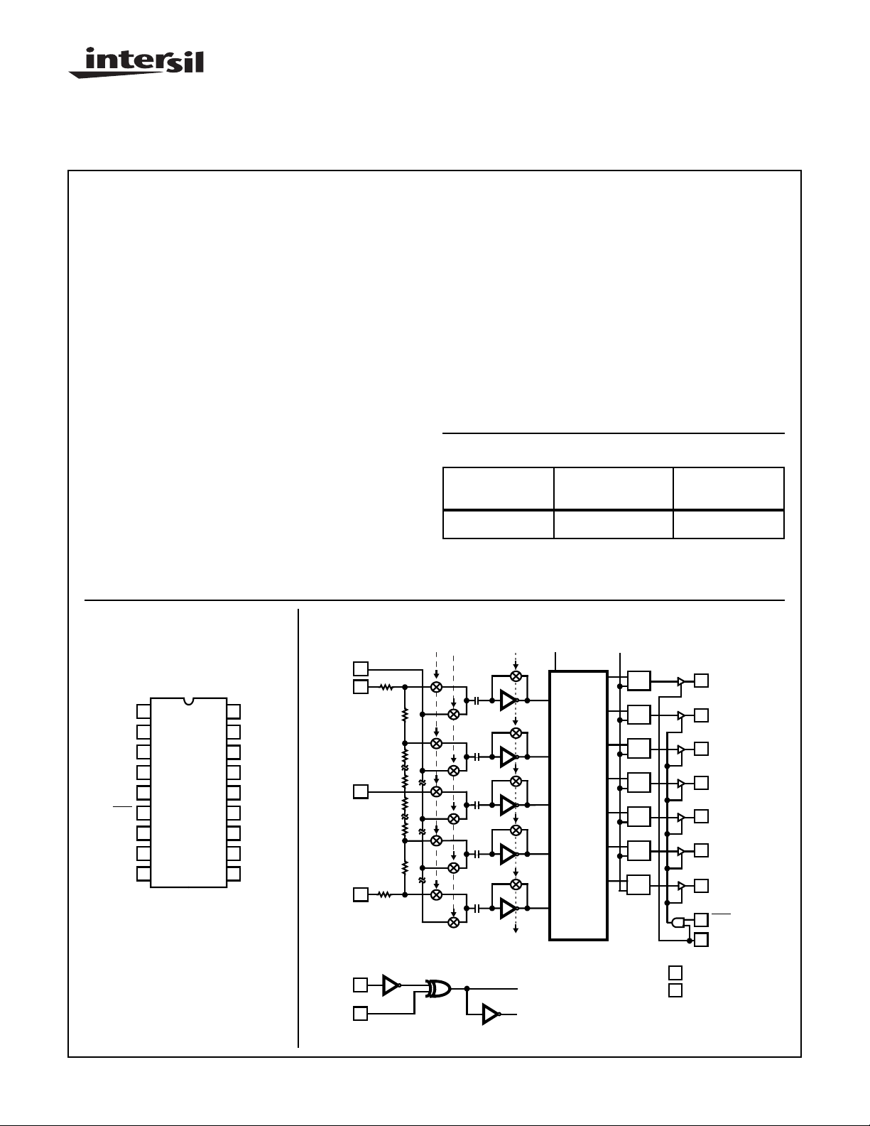
The HI-5701/883 is a monolithic, 6-bit, CMOS Flash Analogto-Digital Converter. It is designed for high speed
applications where wide bandwidth and low power
consumption are essential. Its 30 MSPS speed is made
possible by a parallel architecture which also eliminates the
need for an external sample and hold circuit. The HI-5701/
883 delivers ±0.7 LSB differential nonlinearity while
consuming only 250mW (typical) at 30 MSPS. Microprocessor compatible data output latches are provided which
present valid data to the output bus 1.5 clock cycles after the
convert command is received. An overflow bit is provided to
allow the series connection of two converters to achieve 7-bit
resolution.
Ordering Information
TEMPERATURE
PART NUMBER
HI1-5701T/883 -55oC to +125oC 18 Lead CerDIP
RANGE PACKAGE
• High Speed Data Acquisition Systems
Pinout
D5 (MSB)
OVF
V
SS
NC
CE2
CE1
CLK
PHASE
+
V
REF
HI-5701/883
(18 LEAD CERDIP)
TOP VIEW
1
2
3
4
5
6
7
8
9
18
17
16
15
14
13
12
11
10
D4
D3
1/2R
D2
D1
D0 (LSB)
V
DD
V
IN
V
REF
Functional Block Diagram
-
PHASE
V
V
V
REF
1/2R
REF
CLK
∅2
∅1
11
IN
R/2
9
+
R
R
R
16
R
R
R
10
R/2
7
8
∅1 ∅1 ∅2
COMP
64
COMP
63
COMP
32
AND
COMP
2
COMP
1
2 (SAMPLE)
1 (AUTO BALANCE)
ENCODER LOGIC
COMPARATOR LATCHES
12
3
OVERFLOW
2
(OVF)
1
D5 (MSB)
D4
3
D3
4
5
D2
10
D1
D0 (LSB)
11
CE1
16
CE2
15
D
Q
CL
D
Q
CL
D
Q
CL
D
Q
CL
D
Q
CL
D
Q
CL
D
Q
CL
V
DD
V
SS
CAUTION: These devices are sensitive to electrostatic discharge; follow proper IC Handling Procedures.
407-727-9207
| Copyright © Intersil Corporation 1999
6-14
Spec Number 512031
File Number 3378

HI-5701/883
Pin Description
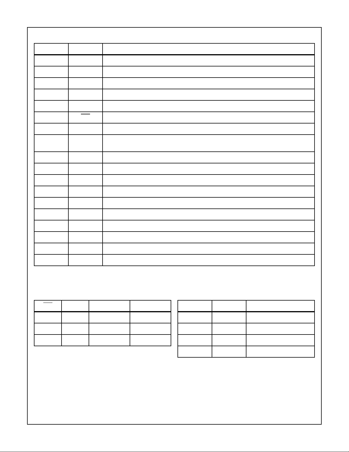
PIN # NAME DESCRIPTION
1 D5 Bit 6, Output (MSB)
2 OVF Overflow, Output
3VSSDigital Ground
4 NC No Connection
5 CE2 Three-State Output Enable Input, Active high (See Truth Table)
6 CE1 Three-State Output Enable Input, Active Low (See Truth Table)
7 CLK Clock Input
8 PHASE Sample Clock Phase Control Input. When Phase is Low, Sample Unknown (φ1) occurs when the Clock
is Low and Auto Balance (φ2) occurs when the Clock is High (See Phase Control Table)
9V
10 V
11 V
12 V
13 D0 Bit 1, Output (LSB)
14 D1 Bit 2, Output
15 D2 Bit 3, Output
16 1/2R Reference Ladder Midpoint
17 D3 Bit 4, Output
18 D4 Bit 5, Output
+ Reference Voltage Positive Input
REF
- Reference Voltage Negative Input
REF
IN
DD
Analog Signal Input
Power Supply, +5V
Chip Enable Truth Table
CE1 CE2 D0 - D5 OVF
0 1 Valid Valid
Phase Control
CLOCK PHASE INTERNAL GENERATION
0 0 Sample Unknown (φ2)
1 1 Three-State Valid
X 0 Three-State Three-State
X = Don’t Care.
0 1 Auto Balance (φ1)
1 0 Auto Balance (φ1)
1 1 Sample Unknown (φ2)
Spec Number 512031
6-15

Specifications HI-5701/883
Absolute Maximum Ratings Thermal Information
Supply Voltage, VDD to VSS . . . . . . . . . . .(V
Analog and Reference Input Pins. .(V
Digital I/O Pins . . . . . . . . . . . . . . . . (V
SS
SS
Operating Temperature Range
HI1-5701T/883 . . . . . . . . . . . . . . . . . . . . . . . . . . -55oC to +125oC
Junction Temperature. . . . . . . . . . . . . . . . . . . . . . . . . . . . . . +175oC
Storage Temperature Range . . . . . . . . . . . . . . . -65oC to +150oC
Lead Temperature (Soldering, 10s) . . . . . . . . . . . . . . . . . . . . 300oC
ESD Clasification . . . . . . . . . . . . . . . . . . . . . . . . . . . . . . . . . Class 1
CAUTION: Stresses above those listed in “Absolute Maximum Ratings” may cause permanent damage to the device. This is a stress only rating and operation
of the device at these or any other conditions above those indicated in the operational sections of this specification is not implied.
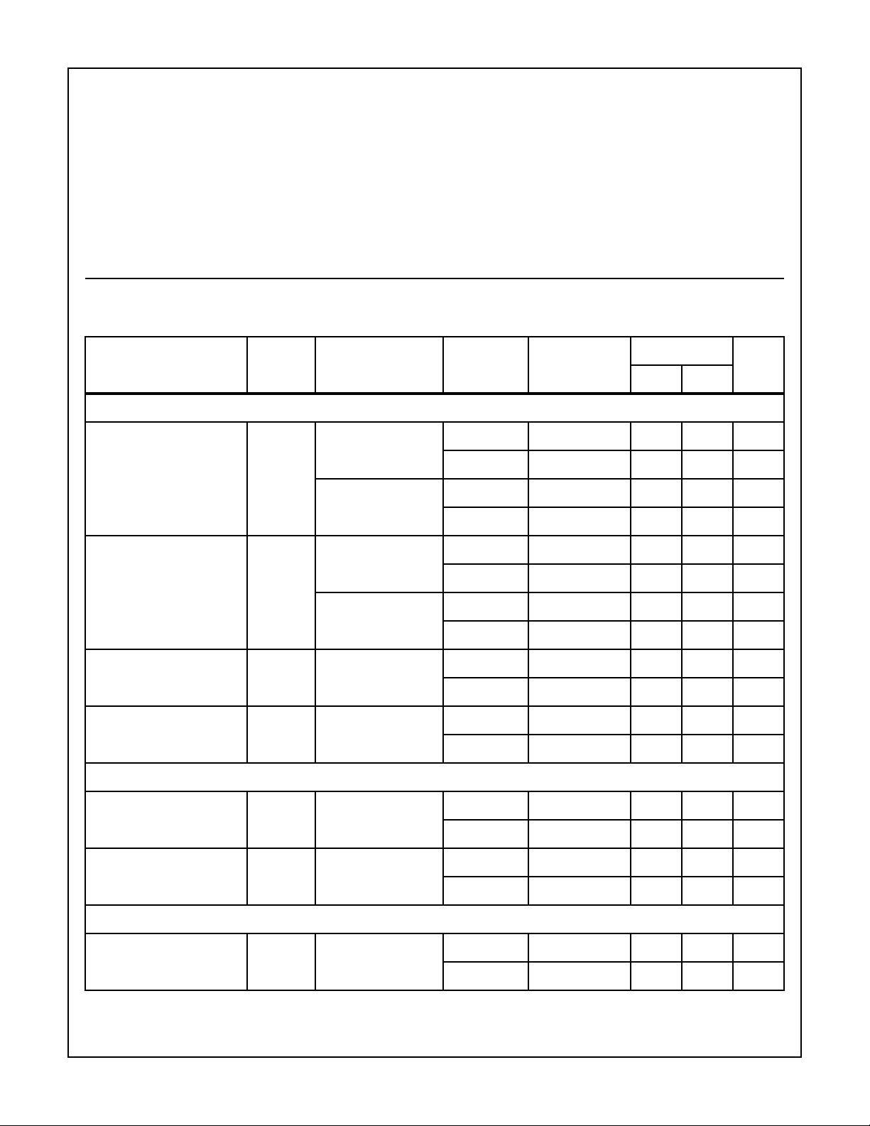
TABLE 1. DC ELECTRICAL PERFORMANCE CHARACTERISTICS
Device Tested at: VDD = +5.0V; V
+ = +4.0V; V
REF
Unless Otherwise Specified.
PARAMETERS SYMBOL CONDITIONS
ACCURACY
- 0.5) < V
SS
- 0.5) < V
- 0.5) < V
< +7.0V
DD
< (VDD +0.5V)
INA
< (VDD +0.5V)
I/O
Thermal Resistance θ
JA
HI1-5701T/883. . . . . . . . . . . . . . . . . . . . . 700C/W 28oC/W
Power Dissipation at +75oC (Note 1)
HI1-5701T/883. . . . . . . . . . . . . . . . . . . . . . . . . . . . . . . . . . 1.4mW
Power Dissipation Derating Factor Above +75oC
HI1-5701T/883. . . . . . . . . . . . . . . . . . . . . . . . . . . . . . . . 14mW/oC
Reliability Information
Transistor Count . . . . . . . . . . . . . . . . . . . . . . . . . . . . . . . . . . . . 4815
Worst Case Density . . . . . . . . . . . . . . . . . . . . . . . . 3.05 x 10⁴A/cm
- = VSS = GND; FS = Specified Clock Frequency at 50% Duty Cycle; CL = 30pF;
REF
LIMITS
GROUP A
SUBGROUP TEMPERATURE
θ
JC
UNITMIN MAX
2
Integral Linearity Error
(Best Fit Method)
Differential Linearity Error
(Guaranteed No Missing
Codes)
Offset Error
VOS FS = 20MHz, fIN = DC 1 +25oC-±2.0 LSB
(Adjustable to Zero)
Full Scale Error
(Adjustable to Zero)
ANALOG INPUT
Analog Input Resistance R
INL FS = 20MHz, fIN = DC 1 +25oC-±1.25 LSB
2, 3 +125oC, -55oC-±2.0 LSB
FS = 30MHz, fIN = DC 1 +25oC-±1.5 LSB
2, 3 +125oC, -55oC-±2.5 LSB
DNL FS = 20MHz, fIN = DC 1 +25oC-±0.6 LSB
2, 3 +125oC, -55oC-±0.75 LSB
FS = 30MHz, fIN = DC 1 +25oC-±0.75 LSB
2, 3 +125oC, -55oC-±1.0 LSB
2, 3 +125oC, -55oC-±2.5 LSB
FSE FS = 20MHz, fIN = DC 1 +25oC-±2.0 LSB
2, 3 +125oC, -55oC-±2.5 LSB
VIN = 4V 1 +25oC4-MΩ
IN
2, 3 +125oC, -55oC4 - MΩ
Analog Input Bias Current I
REFERENCE INPUT
Total Reference Resistance R
VIN= 0V, 4V 1 +25oC ±1.0 µA
B
2, 3 +125oC, -55oC ±1.0 µA
L
1 +25oC 250 - Ω
2, 3 +125oC, -55oC 235 - Ω
Spec Number 512031
6-16
 Loading...