

®
www.BDTIC.com/Intersil
HI-565A
Data Sheet May 2002
High Speed, Monolithic D/A Converter
with Reference
The HI-565A is a fast, 12-bit, current output, digital-to-analog
converter. The monolithic chip includes a precision voltage
reference, thin-film R2R ladder, reference control amplifier
and twelve high speed bipolar current switches.
The Intersil dielectric isolation process provides latch free
operation while minimizing stray capacitance and leakage
currents, to produce an excellent combination of speed and
accuracy. Also, ground currents are minimized to produce a
low and constant current through the ground terminal, which
reduces error due to code dependent ground currents.
HI-565A dice are laser trimmed for a maximum integral
nonlinearity error of ±0.5 LSB at 25
noise buried zener reference is trimmed both for absolute
value and temperature coefficient. Power dissipation is
typically 250mW, with ±15V supplies.
The HI-565A is offered in both commercial and military
grades. See Ordering Information.
o
C. In addition, the low
FN3109.4
Features
• 12-Bit DAC and Reference on a Single Chip
• Pin Compatible With AD565A
• Very High Speed: Settles to ±0.5 LSB in 250ns (Max)
Full Scale Switching Time 30ns (Typ)
• Guaranteed For Operation With ±12V Supplies
• Monotonicity Guaranteed Over Temperature
• Nonlinearity Guaranteed Over Temp (Max). . . . ±0.5 LSB
• Low Gain Drift (Max, DAC Plus Ref) . . . . . . . . .25ppm/oC
• Low Power Dissipation . . . . . . . . . . . . . . . . . . . . .250mW
Applications
• CRT Displays
• High Speed A/D Converters
• Signal Reconstruction
• Waveform Synthesis
Ordering Information
PART NUMBER LINEARITY (INL) LINEARITY (DNL) TEMP. RANGE (oC) PACKAGE PKG. NO.
HI1-565AJD-5 0.50 LSB 0.75 LSB 0 to 75 24 Ld SBDIP D24.6
HI1-565ATD-2 0.25 LSB 0.50 LSB -55 to 125 24 Ld SBDIP D24.6
HI1-565ASD/883 0.50 LSB 0.50 LSB -55 to 125 24 Ld SBDIP D24.6
HI1-565ATD/883 0.25 LSB 0.50 LSB -55 to 125 24 Ld SBDIP D24.6
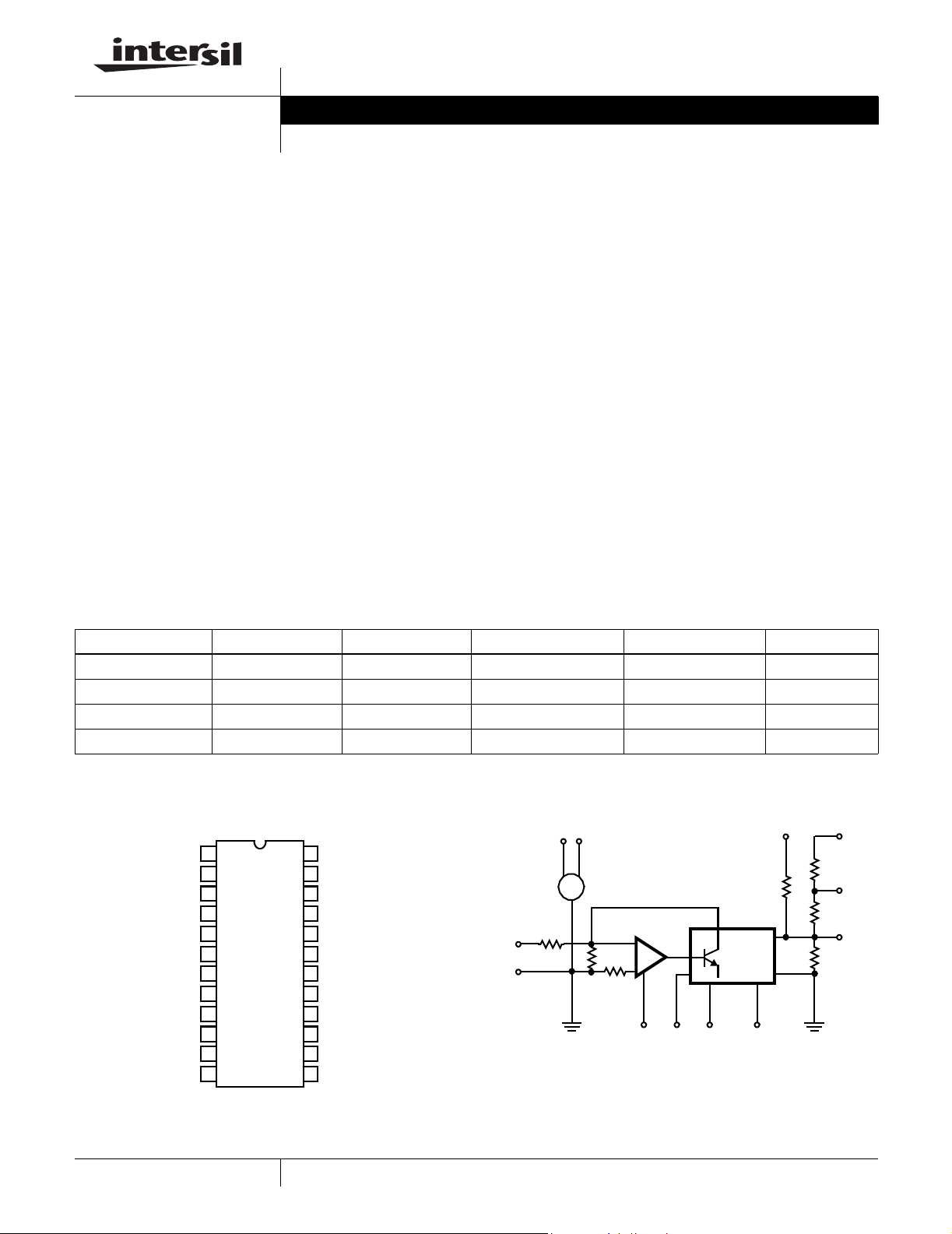
Pinout
REF OUT (+10V)
NC
NC
V
CC
REF GND
REF IN
-V
EE
BIPOLAR R IN
IDAC OUT
10V SPAN R
20V SPAN R
POWER GND
HI-565A (SBDIP)
TOP VIEW
1
2
3
4
5
6
7
8
9
10
11
12
24
BIT 1 (MSB) IN
23
BIT 2 IN
BIT 3 IN
22
21
BIT 4 IN
20
BIT 5 IN
19
BIT 6 IN
18
BIT 7 IN
17
BIT 8 IN
16
BIT 9 IN
15
BIT 10 IN
14
BIT 11 IN
13
BIT 12 (LSB) IN
Functional Diagram
REF
OUT
V
CC
REF
IN
6
5
REF
GND
43
+
-
19.95K
3.5K
3K
HI-565A
0.5mA
I
REF
+
-
712
-V
EE
PWR
GND
BIP. OFF
9.95K
DAC
(4X I
REF
X CODE)
24 . . . . . .13
MSB LSB
8
I
O
2.5K
5K
5K
11
10
9
20V
SPAN
10V
SPAN
OUT
1
CAUTION: These devices are sensitive to electrostatic discharge; follow proper IC Handling Procedures.
1-888-INTERSIL or 321-724-7143
| Intersil (and design) is a registered trademark of Intersil Americas Inc.
Copyright © Intersil Americas Inc. 2002. All Rights Reserved
HI-565A
www.BDTIC.com/Intersil
Absolute Maximum Ratings Thermal Information
VCC to Power GND . . . . . . . . . . . . . . . . . . . . . . . . . . . . . 0V to +18V
V
to Power GND . . . . . . . . . . . . . . . . . . . . . . . . . . . . . 0V to -18V
EE
Voltage on DAC Output (Pin 9) . . . . . . . . . . . . . . . . . . . -3V to +12V
Digital Inputs (Pins 13-24) to Power GND . . . . . . . . . . .-1V to +7.0V
REF In to REF GND. . . . . . . . . . . . . . . . . . . . . . . . . . . . . . . . . ±12V
Bipolar Offset to REF GND . . . . . . . . . . . . . . . . . . . . . . . . . . . ±12V
10V Span R to REF GND . . . . . . . . . . . . . . . . . . . . . . . . . . . . ±12V
20V Span R to REF GND . . . . . . . . . . . . . . . . . . . . . . . . . . . . ±24V
REF Out. . . . . . . . . . . . . . . . . . . . . . Indefinite Short to Power GND,
Momentary Short to V
CC
Operating Conditions
Temperature Ranges
HI1-565AX-2, /883 . . . . . . . . . . . . . . . . . . . . . . . . -55
HI1-565AX-5. . . . . . . . . . . . . . . . . . . . . . . . . . . . . . . . 0
CAUTION: Stresses above those listed in “Absolute Maximum Ratings” may cause permanent damage to the device. This is a stress only rating and operation of the
device at these or any other conditions above those indicated in the operational sections of this specification is not implied.
NOTE:
is measured with the component mounted on an evaluation PC board in free air.
1. θ
JA
o
C to 125oC
o
C to 75oC
Thermal Resistance (Typical, Note 1) θ
SBDIP Package . . . . . . . . . . . . . . . . . . 60 20
Maximum Package Power Dissipation
SBDIP Package . . . . . . . . . . . . . . . . . . . . . . . . . . . . . . . . .500mW
Maximum Junction Temperature. . . . . . . . . . . . . . . . . . . . . . .175
Maximum Storage Temperature Range . . . . . . . . . -65
Maximum Lead Temperature (Soldering 10s). . . . . . . . . . . . .300
Die Characteristics
Transistor Count . . . . . . . . . . . . . . . . . . . . . . . . . . . . . . . . . . . . . 200
Process . . . . . . . . . . . . . . . . . . . . . . . . . . . . . . . . . . . . . . . Bipolar-DI
(oC/W) θJC (oC/W)
JA
o
C to 150oC
o
o
C
C
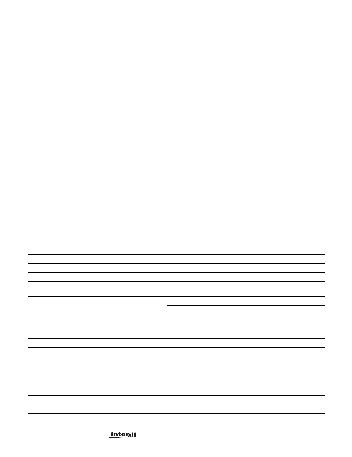
Electrical Specifications T
PARAMETER TEST CONDITIONS
DATA INPUTS (Pins 13 to 24)
Input Voltage Bit ON Logic “1” (T
Input Voltage Bit OFF Logic “0” (T
Logic Current Bit ON Logic “1” (T
Logic Current Bit OFF Logic “0” (T
Resolution (Note 2) 12 - - 12 - - Bits
OUTPUT
Unipolar Current (All Bits ON) -1.6 -2.0 -2.4 -1.6 -2.0 -2.4 mA
Bipolar Current (All Bits ON or OFF) ±0.8 ±1.0 ±1.2 ±0.8 ±1.0 ±1.2 mA
Resistance (Exclusive of Span
Unipolar Offset (25
Bipolar Offset (25
Bipolar Offset (T
/883 Versions Only
Capacitance - 20 - - 20 - pF
Compliance Voltage (T
ACCURACY (Error Relative to Full Scale)
Integral Non-Linearity (25
Integral Non-Linearity
/883 Versions Only
Differential Non-Linearity 25
Differential Non-Linearity T
o
C) -0.05 0.01 0.05 -0.05 0.01 0.05 % of FS
o
C) -0.15 0.05 0.15 -0.1 0.05 0.1 % of FS
MlN
to T
MAX
)
= 25oC, VCC = +15V, VEE = -15V, Unless Otherwise Specified
A
HI-565AJ, HI-565AS HI-565AT
to T
MlN
to T
MlN
to T
MlN
to T
MlN
Resistors) (Note 2)
(Figure 2, R3 = 50Ω) -0.25 0.05 0.25 -0.2 0.05 0.2 % of FS
to T
MIN
o
C)
End Point Method
to T
(T
MIN
End Point Method
o
C-±0.50 ±0.75 - ±0.25 ±0.50 LSB
to T
MIN
) +2.0 - +5.5 +2.0 - +5.5 V
MAX
) - -+0.8- -+0.8 V
MAX
) - 0.01 +1.0 - 0.01 +1.0 µA
MAX
) - -2.0 -20 - -2.0 -20 µA
MAX
1.8K 2.5K 3.2K 1.8K 2.5K 3.2K Ω
-0.07 0.01 0.07 -0.07 0.01 0.07 % of FS
)(Note 2) -1.5 - +10 -1.5 - +10 V
MAX
MAX
MAX
- ±0.25
(0.006)
)
- ±0.50
(0.012)
±0.50
(0.012)
±0.75
(0.018)
MONOTONICITY GUARANTEED
- ±0.12
(0.003)
- ±0.25
(0.006)
±0.25
(0.006)
±0.50
(0.012)
UNITSMIN TYP MAX MIN TYP MAX
LSB
% of FS
LSB
% of FS
2
HI-565A
www.BDTIC.com/Intersil
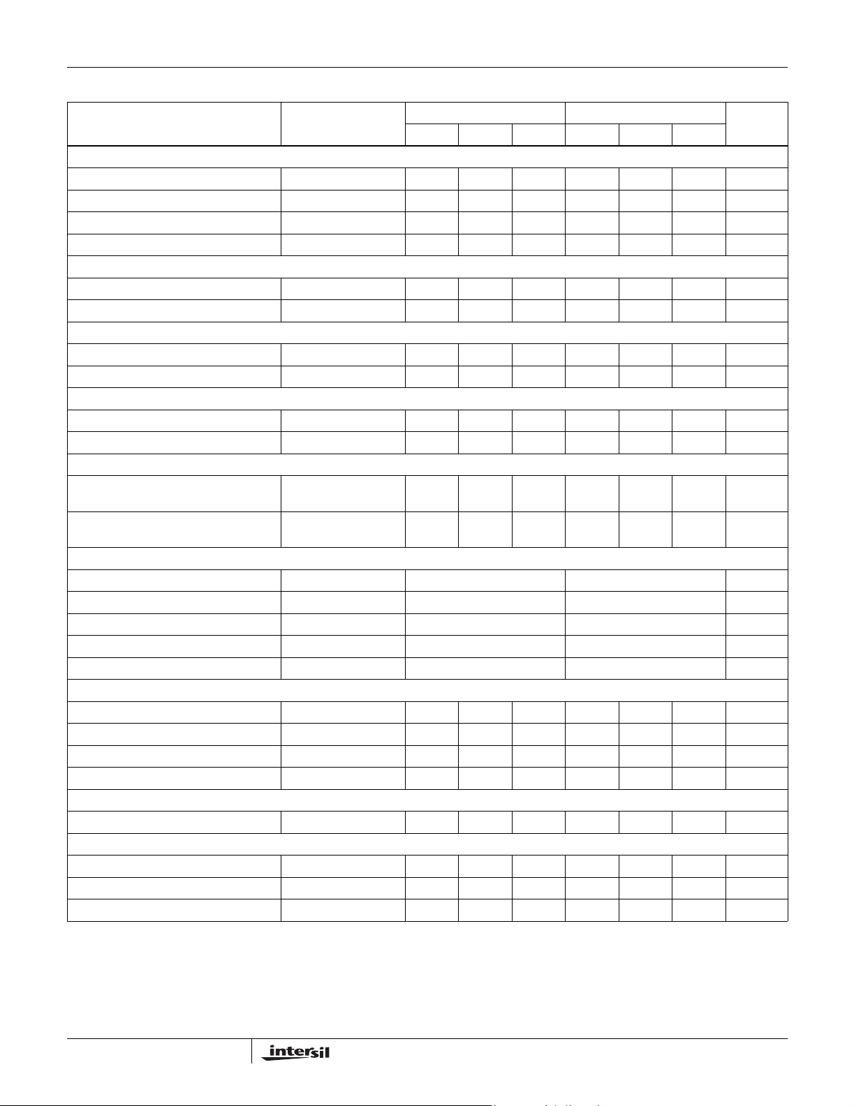
Electrical Specifications T
PARAMETER TEST CONDITIONS
TEMPERATURE COEFFIClENTS
Unipolar Offset Drift - 1 2 - 1 2 ppm/
Bipolar Zero Drift Internal Reference - 5 10 - 5 10 ppm/
Gain Drift, Uni- and Bipolar (Full Scale) Internal Reference - 15 40 - 10 25 ppm/
Differential Nonlinearity Error Drift Int. Ref. - 2 - - 2 - ppm/
SETTLING TIME T0 ±0.5 LSB
With High, Z External Load (Notes 2, 3) - 350 500 - 350 500 ns
With 75Ω External Load (Notes 2, 3) - 150 250 - 150 250 ns
FULL SCALE TRANSITION From 50% of Logic Input to 90% of Analog Output
Rise Time (Note 2) - 15 30 - 15 30 ns
Fall Time (Note 2) - 30 50 - 30 50 ns
POWER REQUIREMENTS
I
CC
I
EE
POWER SUPPLY GAIN SENSITIVITY (Note 4)
V
CC
V
EE
PROGRAMMABLE OUTPUT RANGES (See Table 2)
Unipolar 5 (Note 2) 0 to +5 0 to +5 V
Bipolar 5 (Note 2) -2.5 to +2.5 -2.5 to +2.5 V
Unipolar 10 (Note 2) 0 to +10 0 to +10 V
Bipolar 10 (Note 2) -5 to +5 -5 to +5 V
Bipolar 20 (Note 2) -10 to +10 -10 to +10 V
EXTERNAL ADJUSTMENTS
Gain Error R2 = 50Ω (Figure 2) - ±0.1 ±0.25 - ±0.1 ±0.25 % of FS
Bipolar Zero Error R3 = 50Ω (Figure 3) - ±0.05 ±0.15 - ±0.05 ±0.1 % of FS
Gain Adjustment Range (Figure 1) (Note 2) ±0.25 - - ±0.25 - - % of FS
Bipolar Zero Adjustment Range (Note 2) ±0.15 - - ±0.15 - - % of FS
REFERENCE INPUT
Input Impedance (Note 2) 15K 20K 25K 15K 20K 25K Ω
REFERENCE OUTPUT
Voltage, Commercial Versions 9.90 10.00 10.10 9.90 10.00 10.10 V
Voltage, /883 Versions 9.95 10.00 10.05 9.95 10.00 10.05 V
Current (Available for External Loads) 1.5 2.5 - 1.5 2.5 - mA
NOTES:
2. Guaranteed by characterization or design but not tested over the operating temperature range.
3. See settling time discussion and Figure 3.
4. The Power Supply Gain Sensitivity is tested in reference to a V
= 25oC, VCC = +15V, VEE = -15V, Unless Otherwise Specified (Continued)
A
HI-565AJ, HI-565AS HI-565AT
- 9.0 11.8 - 9.0 11.8 mA
- -9.5 -14.5 - -9.5 -14.5 mA
(+11.4 to +16.5VDC)
All Bits = 2V, Unipolar
(-11.4 to -16.5VDC)
All Bits = 2V, Unipolar
- 3 10 - 3 10 ppm of
- 15 25 - 15 25 ppm of
, VEE of ± 15V.
CC
UNITSMIN TYP MAX MIN TYP MAX
FS/%
FS/%
o
C
o
C
o
C
o
C
3

HI-565A
www.BDTIC.com/Intersil
Definitions of Specifications
Digital Inputs
The HI-565A accepts digital input codes in binary format and
may be user connected for any one of three binary codes.
Straight Binary, Two’s Complement (Note 5), or Offset
Binary, (See Operating Instructions).
TABLE 1.
ANALOG OUTPUT
(NOTE 5)
DIGITAL
INPUT
MSB...LSB
000...000 Zero -FS
100...000
111...111 +FS - 1 LSB +FS - 1 LSB Zero - 1 LSB
011...111 1/2FS - 1 LSB Zero - 1 LSB +FS - 1 LSB
NOTE:
5. Invert MSB with external inverter to obtain Two’s Complement
Coding.
Nonlinearity of a D/A converter is an important measure of
its accuracy. It describes the deviation from an ideal straight
line transfer curve drawn between zero (all bits OFF) and full
scale (all bits ON) (End Point Method).
Differential Nonlinearity for a D/A converter, it is the
difference between the actual output voltage change and the
ideal (1 LSB) voltage change for a one bit change in code. A
Differential Nonlinearity of ±1 LSB or less guarantees
monotonicity; i.e., the output always increases for an
increasing input.
Settling Time is the time required for the output to settle to
within the specified error band for any input code transition.
It is usually specified for a full scale or major carry transition,
settling to within ±0.5 LSB of final value.
Gain Drift is the change in full scale analog output over the
specified temperature range, expressed in parts per million
of full scale range per
measured with respect to 25
temperatures. Gain drift is calculated for both high (T
-25oC) and low ranges (25oC -TL) by dividing the gain error
by the respective change in temperature. The specification is
the larger of the two representing worst-case drift.
Offset Drift is the change in analog output with all bits OFF
over the specified temperature range expressed in parts per
million of full scale range per
is measured with respect to 25
temperatures. Offset Drift is calculated for both high (T
-25oC) and low (25oC -TL) ranges by dividing the offset error
by the respective change in temperature. The specification
given is the larger of the two, representing worst-case drift.
STRAIGHT
BINARY
1
/2FS Zero -FS
o
OFFSET
BINARY
(Full Scale)
C (ppm of FSR/oC). Gain error is
o
C at high (TH) and low (TL)
o
C (ppm of FSR/oC). Offset error
o
C at high (TH) and low (TL)
TWO'S
COMPLEMENT
Zero
H
H
Power Supply Sensitivity is a measure of the change in
gain and offset of the D/A converter resulting from a change
in -15V or +15V supplies. It is specified under DC conditions
and expressed as parts per million of full scale range per
percent of change in power supply (ppm of FSR/%).
Compliance Voltage is the maximum output voltage range
that can be tolerated and still maintain its specified accuracy.
Compliance Limit implies functional operation only, and
makes no claims to accuracy.
Glitch a glitch on the output of a D/A converter is a transient
spike resulting from unequal internal ON-OFF switching
times. Worst case glitches usually occur at half-scale or the
major carry code transition from 011...1 to 100...0 or vice
versa. For example, if turn ON is greater than turn OFF for
011...1 to 100...0, an intermediate state of 000...0 exists,
such that, the output momentarily glitches toward zero
output. Matched switching times and fast switching will
reduce glitches considerably.
Detailed Description
Op Amp Selection
The Hl-565As current output may be converted to voltage
using the standard connections shown in Figures 1 and 2.
The choice of operational amplifier should be reviewed for
each application, since a significant trade-off may be made
between speed and accuracy.
For highest precision, use an HA-5135. This amplifier
contributes negligible error, but requires about 11µs to settle
within ±0.1% following a 10V step.
The Intersil HA-2600/05 is the best all-around choice for this
application, and it settles in 1.5µs (also to ±0.1% following a
10V step). Remember, settling time for the DAC amplifier
combination is the square root of t
are settling times for the DAC and amplifier.
No-Trim Operation
The Hl-565A will perform as specified without calibration
adjustments. To operate without calibration, substitute 50Ω
resistors for the 100Ω trimming potentiometers: In Figure 1
replace R2 with 50Ω also remove the network on pin 8 and
connect 50Ω to ground. For bipolar operation in Figure 2,
replace R3 and R4 with 50Ω resistors.
With these changes, performance is guaranteed as shown
under Specifications, “External Adjustments”. Typical unipolar
zero will be ±0.5
The feedback capacitor, C, must be selected to minimize
settling time.
LSB plus the op amp offset.
Calibration
Calibration provides the maximum accuracy from a
converter by adjusting its gain and offset errors to zero. For
the Hl-565A, these adjustments are similar whether the
current output is used, or whether an external op amp is
D
2
plus t
2
, where tD, tA
A
4

HI-565A
www.BDTIC.com/Intersil
added to convert this current to a voltage. Refer to Table 2
for the voltage output case, along with Figure 1 or Figure 2.
Calibration is a two step process for each of the five output
ranges shown in Table 2. First adjust the negative full scale
(zero for unipolar ranges). This is an offset adjust which
translates the output characteristic, i.e., affects each code by
the same amount.
TABLE 2. OPERATING MODES AND CALIBRATION
CIRCUIT CONNECTIONS CALIBRATION
OUTPUT
MODE
Unipolar
(See Figure 1)
Bipolar
(See Figure 2)
PRANGE PIN 10 TO PIN 11 TO RESlSTOR (R)
0 to +10V V
0 to +5V V
O
O
Pin 10 1.43K All 0’s
Pin 9 1.1K All 0’s
±10V NC V
±5V V
±2.5V V
O
O
Pin 10 1.43K All 0’s
Pin 9 1.1K All 0’s
Next adjust positive FS. This is a gain error adjustment, which
rotates the output characteristic about the negative FS value.
For the bipolar ranges, this approach leaves an error at the
zero code, whose maximum value is the same as for integral
nonlinearity error. In general, only two values of output may
be calibrated exactly; all others must tolerate some error.
Choosing the extreme end points (plus and minus full scale)
minimizes this distributed error for all other codes.
APPLY
INPUT CODE ADJUST
R1
All 1’s
R2
R1
All 1’s
O
1.69K All 0’s
All 1’s
R2
R3
R4
R3
All 1’s
R4
R3
All 1’s
R4
TO SET
V
O
0V
+9.99756V
0V
+4.99878V
-10V
+9.99512V
-5V
+4.99756V
-2.5V
+2.49878V
R2
100Ω
REF
IN
REF
GND
REF OUT
19.95K
6
5
+
-
V
CC
43
10V
3.5K
BIP.
8
OFF.
3K
HI-565A
I
REF
0.5mA
+
-
71224 13
EE
PWR
GND
MSB LSB
-V
DAC
(4 x I
x CODE)
CODE
INPUT
9.95K
REF
5K
5K
I
O
2.5K
FIGURE 1. UNIPOLAR VOLTAGE OUTPUT
11
20V SPAN
10
10V SPAN
9
DAC
OUT
C
-
+
R (SEE
TABLE 2)
100kΩ
V
100Ω
O
R1
50kΩ
+15V
-15V
5

HI-565A
www.BDTIC.com/Intersil
R3
100Ω
HI-565A
I
REF
0.5mA
+
-
71224 13
-V
EE
PWR
GND
R4
100Ω
REF
IN
REF
GND
REF OUT
19.95K
6
5
V
CC
43
+
10V
-
3.5K
3K
FIGURE 2. BIPOLAR VOLTAGE OUTPUT
Settling Time
This is a challenging measurement, in which the result
depends on the method chosen, the precision and quality of
test equipment and the operating configuration of the DAC
(test conditions). As a result, the different techniques in use
by converter manufacturers can lead to consistently different
results. An engineer should understand the advantage and
limitations of a given test method before using the specified
settling time as a basis for design.
The previous approach calls for a strobed comparator to
sense final perturbations of the DAC output waveform. This
gives the LSB a reasonable magnitude (814µV for the
HI-565A), which provides the comparator with enough
overdrive to establish an accurate ±0.5 LSB window about the
final settled value. Also, the required test conditions simulate
the DACs environment for a common application - use in a
successive approximation A/D converter. Considerable
experience has shown this to be a reliable and repeatable
way to measure settling time.
The usual specification is based on a 10V step, produced by
simultaneously switching all bits from off-to-on (t
to-off (t
). The slower of the two cases is specified, as
OFF
measured from 50% of the digital input transition to the final
entry within a window of ±0.5 LSB about the settled value.
Four measurements characterize a given type of DAC:
(a) t
(b) t
(c) t
(d) t
, to final value +0.5 LSB
ON
, to final value -0.5 LSB
ON
, to final value +0.5 LSB
OFF
, to final value -0.5 LSB
OFF
ON
) or on-
BIP.
OFF.
8
11
20V SPAN
9.95K
DAC
I
O
(4 x I
REF
x CODE)
CODE
INPUT
MSB LSB
5K
5K
2.5K
10
9
DAC
OUT
10V SPAN
C
-
+
R(SEE
TABLE 2)
V
O
(Cases (b) and (c) may be eliminated unless the overshoot
exceeds 0.5 LSB). For example, refer to Figure 3 for the
measurement of case (d).
Procedure
As shown in Figure 3B, settling time equals tX plus the
comparator delay (t
• Adjust the delay on generator No. 2 for a tX of several
microseconds. This assures that the DAC output has
settled to its final value.
• Switch on the LSB (+5V).
• Adjust the V
COMPARA TOR OUT. This is indicated by traces of
equal brightness on the oscilloscope display as shown
in Figure 3B. Note DVM reading.
• Switch the LSB to Pulse (P).
• Readjust the V
and note DVM reading. One LSB equals one tenth the
difference in the DVM readings noted above.
• Adjust the V
5 LSBs (DVM reads 10X, so this sets the comparator to
sense the final settled value minus 0.5
Comparator output disappears.
• Reduce generator No. 2 delay until comparator output
reappears, and adjust for “equal brightness”.
• Measure t
time equals t
= 15ns). To measure tX:
D
supply for 50% triggering at
LSB
supply for 50% triggering as before,
LSB
supply to reduce the DVM reading by
LSB
from scope as shown in Figure 3B. Settling
X
+ tD, i.e., tX + 15ns.
X
LSB).
6

HI-565A
www.BDTIC.com/Intersil
(A)
OUT
+5V
GENERATOR
24
23
14
P
13
LSB
~100kHz
PULSE
NO. 1
HI-565A
9.95K
2mA
12
SYNC
TRIG
OUT
5K
5K
2.5K
DVM
IN
GENERATOR
20V ±20%
BIAS
8
11
10
NC
9
5
PULSE
NO. 2
TURN ON
TURN OFF
10
OUT
(B)
SCHOTTKY
DIODES
90
(C)
STROBE
200K
0.1µF
IN (D)
COMP
OUT
V
LSB
SUPPLY
(A)
(B)
(TURN
OFF)
(C)
(D)
+3V
0V
0V
-400mV
2V
0.8V
4V
0V
50%
t
X
50%
DIGITAL
INPUT
-0.5 LSB
DAC
OUTPUT
SETTLING TIME
tD = COMPARATOR DELAY
COMP.
STROBE
EQUAL
BRIGHTNESS
COMP.
OUT
FIGURE 3A. FIGURE 3B.
Other Considerations
Grounds
The Hl-565A has two ground terminals, pin 5 (REF GND)
and pin 12 (PWR GND). These should not be tied together
near the package unless that point is also the system signal
ground to which all returns are connected. (If such a point
exists, then separate paths are required to pins 5 and 12).
The current through pin 5 is near-zero DC (Note 1); but pin
12 carries up to 1.75mA of code-dependent current from bits
1, 2, and 3. The general rule is to connect pin 5 directly to
the system “quiet” point, usually called signal or analog
ground. Connect pin 12 to the local digital or power ground.
Then, of course, a single path must connect the
analog/signal and digital/power grounds.
Layout
Connections to pin 9 (I
for high speed performance. Output capacitance of the DAC
is only 20pF, so a small change or additional capacitance
may alter the op amp’s stability and affect settling time.
Connections to pin 9 should be short and few. Component
leads should be short on the side connecting to pin 9 (as for
feedback capacitor C). See the Settling Time section.
) on the Hl-565A are most critical
OUT
Bypass Capacitors
Power supply bypass capacitors on the op amp will serve
the HI-565A also. If no op amp is used, a 0.01µF ceramic
capacitor from each supply terminal to pin 12 is sufficient,
since supply current variations are small.
Current Cancellation
Current cancellation is a two step process within the
HI-565A in which code dependent variations are eliminated,
then the resulting DC current is supplied internally. First an
auxiliary 9-bit R-2R ladder is driven by the complement of
the DACs input code. Together, the main and auxiliary
ladders draw a continuous 2.25mA from the internal ground
node, regardless of input code. Part of this DC current is
supplied by the zener voltage reference, and the remainder
is sourced from the positive supply via a current mirror which
is laser trimmed for zero current through the external
terminal (pin 5).
7

Die Characteristics
www.BDTIC.com/Intersil
HI-565A
DIE DIMENSIONS:
179 mils x 107 mils x 19 mils ±1 mil
METALLIZATION:
Type: Al
Thickness: 16k
Å ±2kÅ
Metallization Mask Layout
V
OUT
REF
V
REF
GND
V+
HI-565A
PASSIVATION:
Type: Nitride Over Silox
Nitride Thickness: 3.5k
Å ±0.5kÅ
Silox Thickness: 12kÅ ±1.5kÅ
WORST CASE CURRENT DENSITY:
5
2
0.75 x 10
A/cm
TRANSISTOR COUNT:
200
(MSB)
BIT 1
BIT 2
BIT 3
BIT 4
V
REF
BIPOLAR
12
IDAC
OUT
10V
SPAN
BIT 5
IN
-V
S
20V
SPAN
POWER
GND
(LSB)
BIT 11BIT 12
BIT 6
BIT 7
BIT 8
BIT 9
BIT 10
8

HI-565A
www.BDTIC.com/Intersil
Ceramic Dual-In-Line Metal Seal Packages (SBDIP)
LEAD FINISH
c1
-A-
-B-
S
bbb C A - B
BASE
PLANE
SEATING
PLANE
S1
b2
b
ccc
CA - BM
NOTES:
1. Index area: A notch or a pin one identification mark shall be located adjacent to pin one and shall be located within the shaded
area shown. The manufacturer’s identification shall not be used
as a pin one identification mark.
2. The maximum limits of lead dimensions b and c or M shall be
measured at the centroid of the finished lead surfaces, when
solder dip or tin plate lead finish is applied.
3. Dimensions b1 and c1 apply to lead base metal only. Dimension
M applies to lead plating and finish thickness.
4. Corner leads (1, N, N/2, and N/2+1) may be configured with a
partial lead paddle. For this configuration dimension b3 replaces
dimension b2.
5. Dimension Q shall be measured from the seating plane to the
base plane.
6. Measure dimension S1 at all four corners.
7. Measure dimension S2 from the top of the ceramic body to the
nearest metallization or lead.
8. N is the maximum number of terminal positions.
9. Braze fillets shall be concave.
10. Dimensioning and tolerancing per ANSI Y14.5M - 1982.
11. Controlling dimension: INCH.
D
A
A
e
DS S
-DBASE
E
S
S
D
Q
S2
-C-
aaa
METAL
b1
M
(b)
SECTION A-A
A
L
eA/2
CA - BM DS S
(c)
M
eA
c
D24.6 MIL-STD-1835 CDIP2-T24 (D-3, CONFIGURATION C)
24 LEAD CERAMIC DUAL-IN-LINE METAL SEAL PACKAGE
INCHES MILLIMETERS
SYMBOL
A - 0.225 - 5.72 -
b 0.014 0.026 0.36 0.66 2
b1 0.014 0.023 0.36 0.58 3
b2 0.045 0.065 1.14 1.65 b3 0.023 0.045 0.58 1.14 4
c 0.008 0.018 0.20 0.46 2
c1 0.008 0.015 0.20 0.38 3
D - 1.290 - 32.77 E 0.500 0.610 12.70 15.49 -
e 0.100 BSC 2.54 BSC eA 0.600 BSC 15.24 BSC -
eA/2 0.300 BSC 7.62 BSC -
L 0.120 0.200 3.05 5.08 -
Q 0.015 0.075 0.38 1.91 5
S1 0.005 - 0.13 - 6
S2 0.005 - 0.13 - 7
o
α
aaa - 0.015 - 0.38 bbb - 0.030 - 0.76 ccc - 0.010 - 0.25 -
M - 0.0015 - 0.038 2
N24 248
90
105
o
90
o
105
NOTESMIN MAX MIN MAX
o
Rev. 0 4/94
-
All Intersil semiconductor products are manufactured, assembled and tested under ISO9000 quality systems certification.
Intersil semiconductor products are sold b y de scr ip tion on ly. In tersil Corporation reserves the right to make changes in circuit design and/or specifications at any time without notice. Accordingly, the reader is cautioned to verify that data sheets are current before placing orders. Information furnished by Intersil is believed to be accurate and
reliable. However, no responsibility is assumed by Intersil or its subsidiaries for its use; nor for any infringements of patents or other rights of third parties which may result
from its use. No license is granted by implication or othe rwise under any patent or patent righ ts of Intersil or its subsidiaries.
For information regarding Intersil Corporation and its products, see web site www.intersil.com
9
 Loading...