Intersil Corporation HI-565A Datasheet

HI-565A
Data Sheet June 1999
High Speed, Monolithic D/A Converter
with Reference
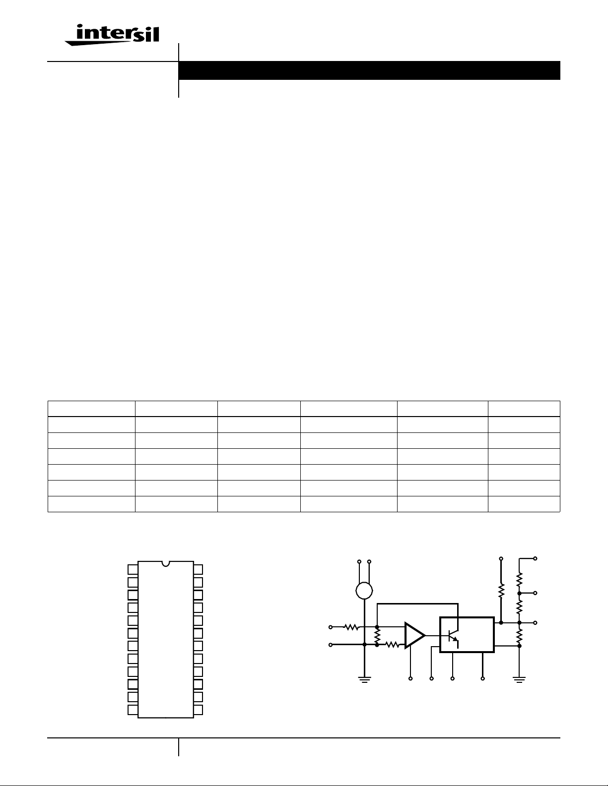
The HI-565A is a fast,12-bit,currentoutput,digital-to-analog
converter. The monolithic chip includes a precision voltage
reference, thin-film R2R ladder, reference control amplifier
and twelve high speed bipolar current switches.
The Intersil dielectric isolation process provides latch free
operation while minimizing stray capacitance and leakage
currents, to produce an excellent combination of speed and
accuracy. Also, ground currents are minimized to produce a
low and constant current through the ground terminal, which
reduces error due to code dependent ground currents.
HI-565A dice are laser trimmed for a maximum integral
nonlinearity error of ±0.5 LSB at 25
noise buried zener reference is trimmed both for absolute
value and temperature coefficient. Power dissipation is
typically 250mW, with ±15V supplies.
The HI-565A is offered in both commercial and military
grades. See Ordering Information.
o
C. In addition, the low
File Number 3109.2
Features
• 12-Bit DAC and Reference on a Single Chip
• Pin Compatible With AD565A
• Very High Speed: Settles to ±0.5 LSB in 250ns (Max)
Full Scale Switching Time 30ns (Typ)
• Guaranteed For Operation With ±12V Supplies
• Monotonicity Guaranteed Over Temperature
• Nonlinearity Guaranteed Over Temp (Max) . . . . ±0.5 LSB
• Low Gain Drift (Max, DAC Plus Ref) . . . . . . . . .25ppm/
o
• Low Power Dissipation . . . . . . . . . . . . . . . . . . . . .250mW
Applications
• CRT Displays
• High Speed A/D Converters
• Signal Reconstruction
• Waveform Synthesis
C
Ordering Information
PART NUMBER LINEARITY (INL) LINEARITY (DNL) TEMP. RANGE (oC) PACKAGE PKG. NO.
HI1-565AJD-5 0.50 LSB 0.75 LSB 0 to 75 24 Ld SBDIP D24.6 HI1-565AKD-5 0.25 LSB 0.50 LSB 0 to 75 24 Ld SBDIP D24.6 HI1-565ASD-2 0.50 LSB 0.75 LSB -55 to 125 24 Ld SBDIP D24.6 HI1-565ATD-2 0.25 LSB 0.50 LSB -55 to 125 24 Ld SBDIP D24.6 HI1-565ASD/883 0.50 LSB 0.50 LSB -55 to 125 24 Ld SBDIP D24.6 HI1-565ATD/883 0.25 LSB 0.50 LSB -55 to 125 24 Ld SBDIP D24.6
Pinout
REF OUT (+10V)
NC
NC
V
CC
REF GND
REF IN
-V
BIPOLAR R IN
IDAC OUT
10V SPAN R
20V SPAN R
POWER GND
HI-565A (SBDIP)
TOP VIEW
1
2
3
4
5
6
7
EE
8
9
10
11
12
24
BIT 1 (MSB) IN
BIT 2 IN
23
BIT 3 IN
22
BIT 4 IN
21
BIT 5 IN
20
BIT 6 IN
19
BIT 7 IN
18
BIT 8 IN
17
BIT 9 IN
16
BIT 10 IN
15
BIT 11 IN
14
BIT 12 (LSB) IN
13
Functional Diagram
REF
OUT
V
CC
REF
IN
6
5
REF
GND
43
+
-
19.95K
3.5K
3K
I
REF
HI-565A
0.5mA
+
-
712
-VEEPWR
GND
BIP. OFF
9.95K
DAC
(4X I
REF
X CODE)
24 . . . . . .13
MSB LSB
8
I
O
2.5K
5K
5K
11
10
9
20V
SPAN
10V
SPAN
OUT
1
CAUTION: These devices are sensitive to electrostatic discharge; follow proper IC Handling Procedures.
1-888-INTERSIL or 321-724-7143
| Copyright © Intersil Corporation 1999

HI-565A
Absolute Maximum Ratings Thermal Information
VCC to Power GND . . . . . . . . . . . . . . . . . . . . . . . . . . . . .0V to +18V
VEE to Power GND . . . . . . . . . . . . . . . . . . . . . . . . . . . . . 0V to -18V
Voltage on DAC Output (Pin 9) . . . . . . . . . . . . . . . . . . . -3V to +12V
Digital Inputs (Pins 13-24) to Power GND . . . . . . . . . . .-1V to +7.0V
REF In to REF GND. . . . . . . . . . . . . . . . . . . . . . . . . . . . . . . . . ±12V
Bipolar Offset to REF GND . . . . . . . . . . . . . . . . . . . . . . . . . . . ±12V
10V Span R to REF GND . . . . . . . . . . . . . . . . . . . . . . . . . . . . ±12V
20V Span R to REF GND . . . . . . . . . . . . . . . . . . . . . . . . . . . . ±24V
REF Out. . . . . . . . . . . . . . . . . . . . . . .Indefinite Short to Power GND
Momentary Short to V
CC
Operating Conditions
Temperature Ranges
HI-565AS, T-2. . . . . . . . . . . . . . . . . . . . . . . . . . . . -55oC to 125oC
H1-565AJ, K-5 . . . . . . . . . . . . . . . . . . . . . . . . . . . . . . 0oC to 75oC
CAUTION: Stresses above those listed in “Absolute Maximum Ratings” may cause permanent damage to the device. This is a stress only rating and operation of the
device at these or any other conditions above those indicated in the operational sections of this specification is not implied.
NOTE:
1. θJA is measured with the component mounted on an evaluation PC board in free air.
Thermal Resistance (Typical, Note 1) θJA (oC/W) θJC (oC/W)
SBDIP Package . . . . . . . . . . . . . . . . . . 75 30
Maximum Package Power Dissipation
SBDIP Package . . . . . . . . . . . . . . . . . . . . . . . . . . . . . . . . .500mW
Maximum Junction Temperature . . . . . . . . . . . . . . . . . . . . . . .175oC
Maximum Storage Temperature Range. . . . . . . . . . -65oC to 150oC
Maximum Lead Temperature (Soldering 10s) . . . . . . . . . . . . .300oC
Die Characteristics
Transistor Count. . . . . . . . . . . . . . . . . . . . . . . . . . . . . . . . . . . . . .200
Process . . . . . . . . . . . . . . . . . . . . . . . . . . . . . . . . . . . . . . .Bipolar-DI
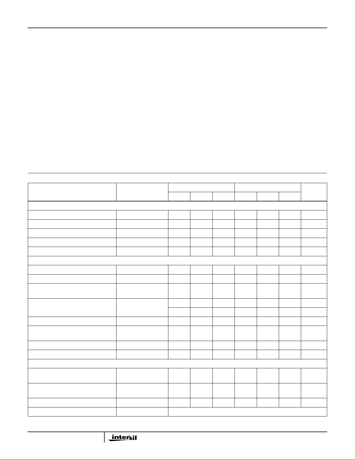
Electrical Specifications T
= 25oC, VCC = +15V, VEE = -15V, Unless Otherwise Specified
A
HI-565AJ, HI565AS HI-565AK, HI-565AT
PARAMETER TEST CONDITIONS
UNITSMIN TYP MAX MIN TYP MAX
DATA INPUTS (Pins 13 to 24)
Input Voltage Bit ON Logic “1” (T
Input Voltage Bit OFF Logic “0” (T
Logic Current Bit ON Logic “1” (T
Logic Current Bit OFF Logic “0” (T
MlN
MlN
MlN
MlN
to T
to T
to T
to T
) +2.0 - +5.5 +2.0 - +5.5 V
MAX
) - - +0.8 - - +0.8 V
MAX
) - 0.01 +1.0 - 0.01 +1.0 µA
MAX
) - -2.0 -20 - -2.0 -20 µA
MAX
Resolution (Note 2) 12 - - 12 - - Bits
OUTPUT
Unipolar Current (All Bits ON) -1.6 -2.0 -2.4 -1.6 -2.0 -2.4 mA Bipolar Current (All Bits ON or OFF) ±0.8 ±1.0 ±1.2 ±0.8 ±1.0 ±1.2 mA Resistance (Exclusive of Span
1.8K 2.5K 3.2K 1.8K 2.5K 3.2K Ω
Resistors) (Note 2)
o
Unipolar Offset (25
C) -0.05 0.01 0.05 -0.05 0.01 0.05 % of FS
-0.07 0.01 0.07 -0.07 0.01 0.07 % of FS
o
Bipolar Offset (25
Bipolar Offset (T
C) -0.15 0.05 0.15 -0.1 0.05 0.1 % of FS
MlN
to T
MAX
)
(Figure 2, R3= 50Ω) -0.25 0.05 0.25 -0.2 0.05 0.2 % of FS
/883 Versions Only
Capacitance - 20 - - 20 - pF
to T
Compliance Voltage (T
MIN
)(Note 2) -1.5 - +10 -1.5 - +10 V
MAX
ACCURACY (Error Relative to Full Scale)
Integral Non-Linearity (25oC)
End Point Method
Integral Non-Linearity
/883 Versions Only
Differential Non-Linearity 25
Differential Non-Linearity T
(T
MIN
End Point Method
o
C-±0.50 ±0.75 - ±0.25 ±0.50 LSB
MIN
to T
to T
MAX
MAX
)
- ±0.25
(0.006)
- ±0.50
(0.012)
±0.50
(0.012)
±0.75
(0.018)
- ±0.12
(0.003)
- ±0.25
(0.006)
MONOTONICITY GUARANTEED
±0.25
(0.006)
±0.50
(0.012)
LSB
% of FS
LSB
% of FS
2

HI-565A
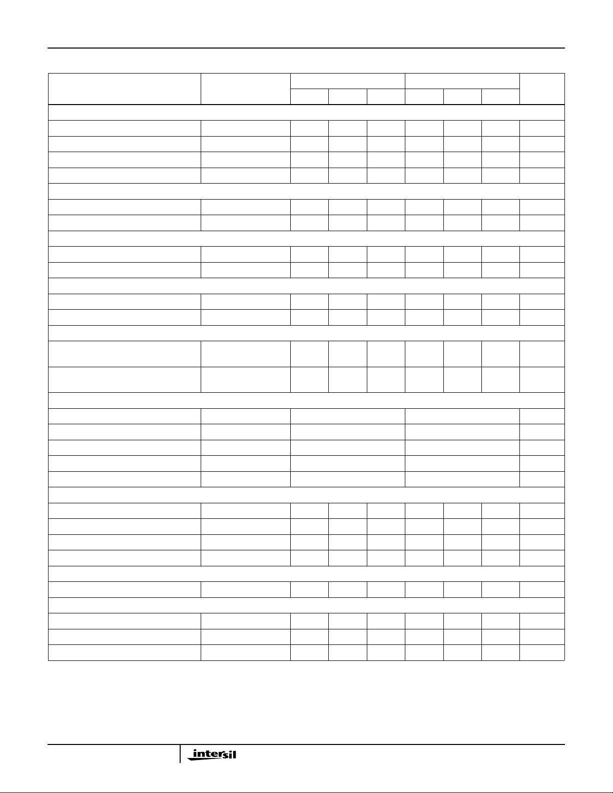
Electrical Specifications T
= 25oC, VCC = +15V, VEE = -15V, Unless Otherwise Specified (Continued)
A
HI-565AJ, HI565AS HI-565AK, HI-565AT
PARAMETER TEST CONDITIONS
UNITSMIN TYP MAX MIN TYP MAX
TEMPERATURE COEFFIClENTS
Unipolar Offset Drift - 1 2 - 1 2 ppm/
Bipolar Zero Drift Internal Reference - 5 10 - 5 10 ppm/
Gain Drift, Uni- and Bipolar (Full Scale) Internal Reference - 15 40 - 10 25 ppm/
Differential Nonlinearity Error Drift Int. Ref. - 2 - - 2 - ppm/
SETTLING TIME T0 ±0.5 LSB
With High, Z External Load (Notes 2, 3) - 350 500 - 350 500 ns
With 75Ω External Load (Notes 2, 3) - 150 250 - 150 250 ns
FULL SCALE TRANSITION From 50% of Logic Input to 90% of Analog Output
Rise Time (Note 2) - 15 30 - 15 30 ns
Fall Time (Note 2) - 30 50 - 30 50 ns
POWER REQUIREMENTS
I
I
CC
EE
- 9.0 11.8 - 9.0 11.8 mA
- -9.5 -14.5 - -9.5 -14.5 mA POWER SUPPLY GAIN SENSITIVITY (Note 4) V
CC
(+11.4 to +16.5VDC)
All Bits = 2V, Unipolar
V
EE
(-11.4 to -16.5VDC)
All Bits = 2V, Unipolar
- 3 10 - 3 10 ppm of
FS/%
- 15 25 - 15 25 ppm of
FS/% PROGRAMMABLE OUTPUT RANGES (See Table 2) Unipolar 5 (Note 2) 0 to +5 0 to +5 V Bipolar 5 (Note 2) -2.5 to +2.5 -2.5 to +2.5 V Unipolar 10 (Note 2) 0 to +10 0 to +10 V Bipolar 10 (Note 2) -5 to +5 -5 to +5 V Bipolar 20 (Note 2) -10 to +10 -10 to +10 V
EXTERNAL ADJUSTMENTS
Gain Error R2 = 50Ω (Figure 2) - ±0.1 ±0.25 - ±0.1 ±0.25 % of FS Bipolar Zero Error R3 = 50Ω (Figure 3) - ±0.05 ±0.15 - ±0.05 ±0.1 % of FS Gain Adjustment Range (Figure 1) (Note 2) ±0.25 - - ±0.25 - - % of FS Bipolar Zero Adjustment Range (Note 2) ±0.15 - - ±0.15 - - % of FS
REFERENCE INPUT
Input Impedance (Note 2) 15K 20K 25K 15K 20K 25K -
REFERENCE OUTPUT
Voltage, Commercial Versions 9.90 10.00 10.10 9.90 10.00 10.10 V Voltage, /883 Versions 9.95 10.00 10.05 9.95 10.00 10.05 V Current (Available for External Loads) 1.5 2.5 - 1.5 2.5 - mA
NOTES:
2. Guaranteed by characterization or design but not tested over the operating temperature range.
3. See settling time discussion and Figure 3.
4. The Power Supply Gain Sensitivity is tested in reference to a V
, VEE of ± 15V.
CC
o
C
o
C
o
C
o
C
3
 Loading...