HI-539
Data Sheet July 1999
Precision, 4-Channel, Low-Level,
Differential Multiplexer
The Intersil HI-539 is a monolithic, 4-Channel, differential
multiplexer. Two digital inputs are provided for channel
selection, plus an Enable input to disconnect all channels.
Performance is guaranteed for each channel over the
voltage range ±10V, but is optimized for low level differential
signals. Leakage current, for example, which varies slightly
with input voltage, has its distribution centered at zero input
volts.
In most monolithic multiplexers, the net differential offset due
to thermal effects becomes significant for low level signals.
This problem is minimized in the HI-539 by symmetrical
placement of critical circuitry with respect to the few heat
producing devices.
Supply voltages are ±15V and power consumption is only
2.5mW.
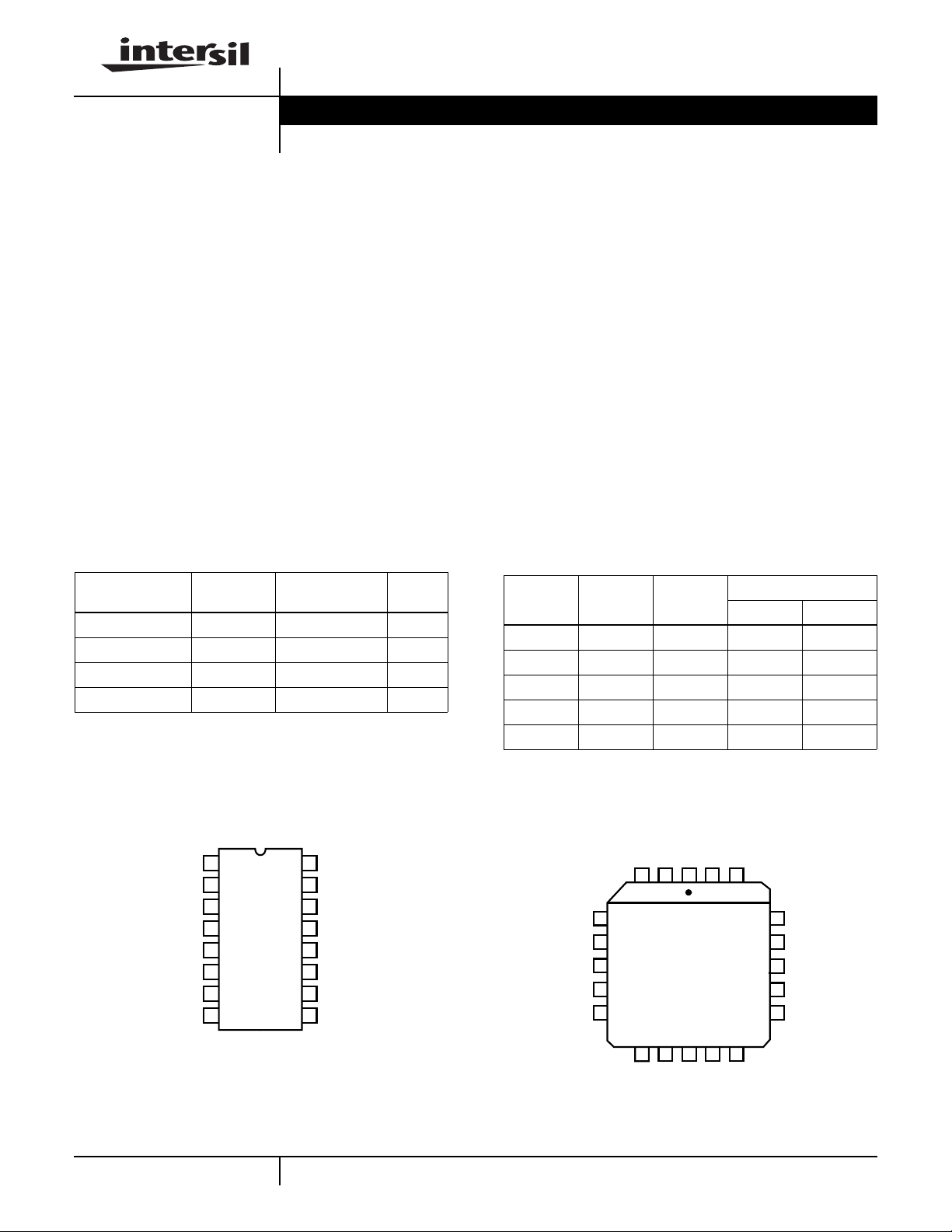
Ordering Information
TEMP.
PART NUMBER
RANGE (oC) PACKAGE
HI1-0539-5 0 to 75 16 Ld CERDIP F16.3
HI1-0539-8 -55 to 125 16 Ld CERDIP F16.3
HI3-0539-5 0 to 75 16 Ld PDIP E16.3
HI4P0539-5 0 to 75 20 Ld PLCC N20.35
PKG.
NO.
File Number
3149.2
Features
• Differential Performance, Typical:
-Low∆r
-Low∆I
, 125oC . . . . . . . . . . . . . . . . . . . . . . . . . .5.5Ω
ON
, 125oC. . . . . . . . . . . . . . . . . . . . . . . 0.6nA
D(ON)
-Low∆ Charge Injection . . . . . . . . . . . . . . . . . . . . 0.1pC
- Low Crosstalk . . . . . . . . . . . . . . . . . . . . . . . . . . . -124dB
• Settling Time, ±0.01% . . . . . . . . . . . . . . . . . . . . . . .900ns
• Wide Supply Range . . . . . . . . . . . . . . . . . . . ±5V to ±18V
• Break-Before-Make Switching
• No Latch-Up
Applications
• Low Level Data Acquisition
• Precision Instrumentation
• Test Systems
TRUTH TABLE
ON CHANNEL TO
EN A
1
L X X None None
HLL1A1B
HLH2A2B
HHL3A3B
H H H 4A 4B
A
0
OUT A OUT B
Pinouts
A
EN
IN 1A
IN 2A
IN 3A
IN 4A
OUT A
(CERDIP, PDIP)
TOP VIEW
1
0
2
3
V-
4
5
6
7
8
HI-539
1
16
15
14
13
12
11
10
9
A
1
GND
V+
IN 1B
IN 2B
IN 3B
IN 4B
OUT B
HI-539
(PLCC)
TOP VIEW
0
A
EN
4
V-
IN 1A
5
6
NC
IN 2A
7
IN 3A
8
9
10 11 12 13
IN 4A
OUT ANCOUT B
CAUTION: These devices are sensitive to electrostatic discharge; follow proper IC Handling Procedures.
http://www.intersil.com or 407-727-9207
1
A
NC
GND
193 2 201
18
V+
17
IN 1B
16
NC
15
IN 2B
IN 3B
14
IN 4B
| Copyright © Intersil Corporation 1999

HI-539
Absolute Maximum Ratings Thermal Information
V+ to V- . . . . . . . . . . . . . . . . . . . . . . . . . . . . . . . . . . . . . . . . . . . 40V
V+ or V- to GND. . . . . . . . . . . . . . . . . . . . . . . . . . . . . . . . . . . . . 20V
Analog Signal (VIN, V
). . . . . . . . . . . . . . . . . . . . . . . . . . V- to V+
OUT
Digital Input Voltage (VEN, VA) . . . . . . . . . . . . . . . . . . . . . . V- to V+
Analog Current (IN or OUT). . . . . . . . . . . . . . . . . . . . . . . . . . . 20mA
Operating Conditions
Temperature Range
HI-539-8 . . . . . . . . . . . . . . . . . . . . . . . . . . . . . . . . -55oC to 125oC
HI-539-5 . . . . . . . . . . . . . . . . . . . . . . . . . . . . . . . . . . 0oC to 75oC
CAUTION: Stresses above those listed in “Absolute Maximum Ratings” may cause permanent damage to the device. This is a stress only rating and operationofthe
device at these or any other conditions above those indicated in the operational sections of this specification is not implied.
NOTE:
1. θJA is measured with the component mounted on an evaluation PC board in free air.
Thermal Resistance (Typical, Note 1) θJA (oC/W) θJC (oC/W)
CERDIP Package. . . . . . . . . . . . . . . . . 85 32
PDIP Package . . . . . . . . . . . . . . . . . . . 90 N/A
PLCC Package. . . . . . . . . . . . . . . . . . . 80 N/A
Maximum Junction Temperature
Ceramic Package. . . . . . . . . . . . . . . . . . . . . . . . . . . . . . . . 175oC
Plastic Package . . . . . . . . . . . . . . . . . . . . . . . . . . . . . . . . . 150oC
Maximum Storage Temperature Range. . . . . . . . . . -65oC to 150oC
Maximum Lead Temperature (Soldering 10s) . . . . . . . . . . . . .300oC
(PLCC - Lead Tips Only)
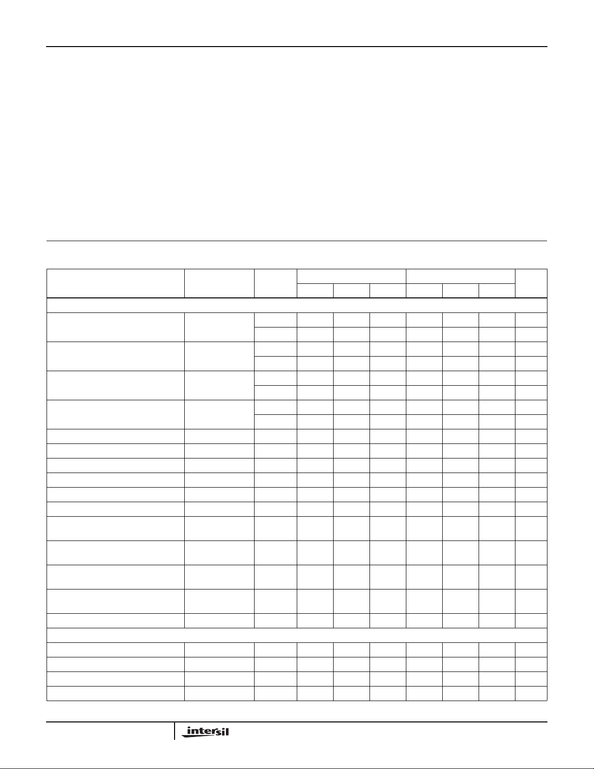
Electrical Specifications Supplies = ±15V, V
= 4V, VAH (Logic Level High) = 4V, VAL (Logic Level Low) = 0.8V,
EN
Unless Otherwise Specified
-8 -5
UNITSMIN TYP MAX MIN TYP MAX
PARAMETER
TEST
CONDITIONS
TEMP
(oC)
DYNAMIC CHARACTERISTICS
Access Time, t
A
25 - 250 750 - 250 750 ns
Full - - 1,000 - - 1,000 ns
Break-Before-Make Delay, t
OPEN
25 30 85 - 30 85 - ns
Full 30 - - 30 - - ns
Enable Delay (ON), t
ON(EN)
25 - 250 750 - 250 750 ns
Full - - 1,000 - - 1,000 ns
Enable Delay (OFF), t
OFF(EN)
25 - 160 650 - 160 650 ns
Full - - 900 - - 900 ns
Settling Time To 0.01% 25 - 0.9 - - 0.9 - µs
Charge Injection (Output) Full - 3 - - 3 - pC
∆ Charge Injection (Output) Full - 0.1 - - 0.1 - pC
Charge Injection (Input) Full - 10 - - 10 - pC
Differential Crosstalk Note 4 25 - -124 - - -124 - dB
Single Ended Crosstalk Note 4 25 - -100 - - -100 - dB
Channel Input Capacitance,
C
S(OFF)
Channel Output Capacitance,
C
D(OFF)
Channel On Output Capacitance,
C
D(ON)
Input to Output Capacitance,
C
DS(OFF)
Digital Input Capacitance, C
A
Note 5 Full - 0.08 - - 0.08 - pF
Full - 5 - - 5 - pF
Full - 7 - - 7 - pF
Full - 17 - - 17 - pF
Full - 3 - - 3 - pF
DIGITAL INPUT CHARACTERISTICS
Input Low Threshold, V
Input High Threshold, V
AL
AH
Input Leakage Current (High), I
Input Leakage Current (Low), I
AH
AL
Full - - 0.8 - - 0.8 V
Full 4.0 - - 4.0 - - V
Full - - 1 - - 1 µA
Full - - 1 - - 1 µA
2

HI-539
Electrical Specifications Supplies = ±15V, V
= 4V, VAH (Logic Level High) = 4V, VAL (Logic Level Low) = 0.8V,
EN
Unless Otherwise Specified (Continued)
-8 -5
UNITSMIN TYP MAX MIN TYP MAX
PARAMETER
TEST
CONDITIONS
TEMP
(oC)
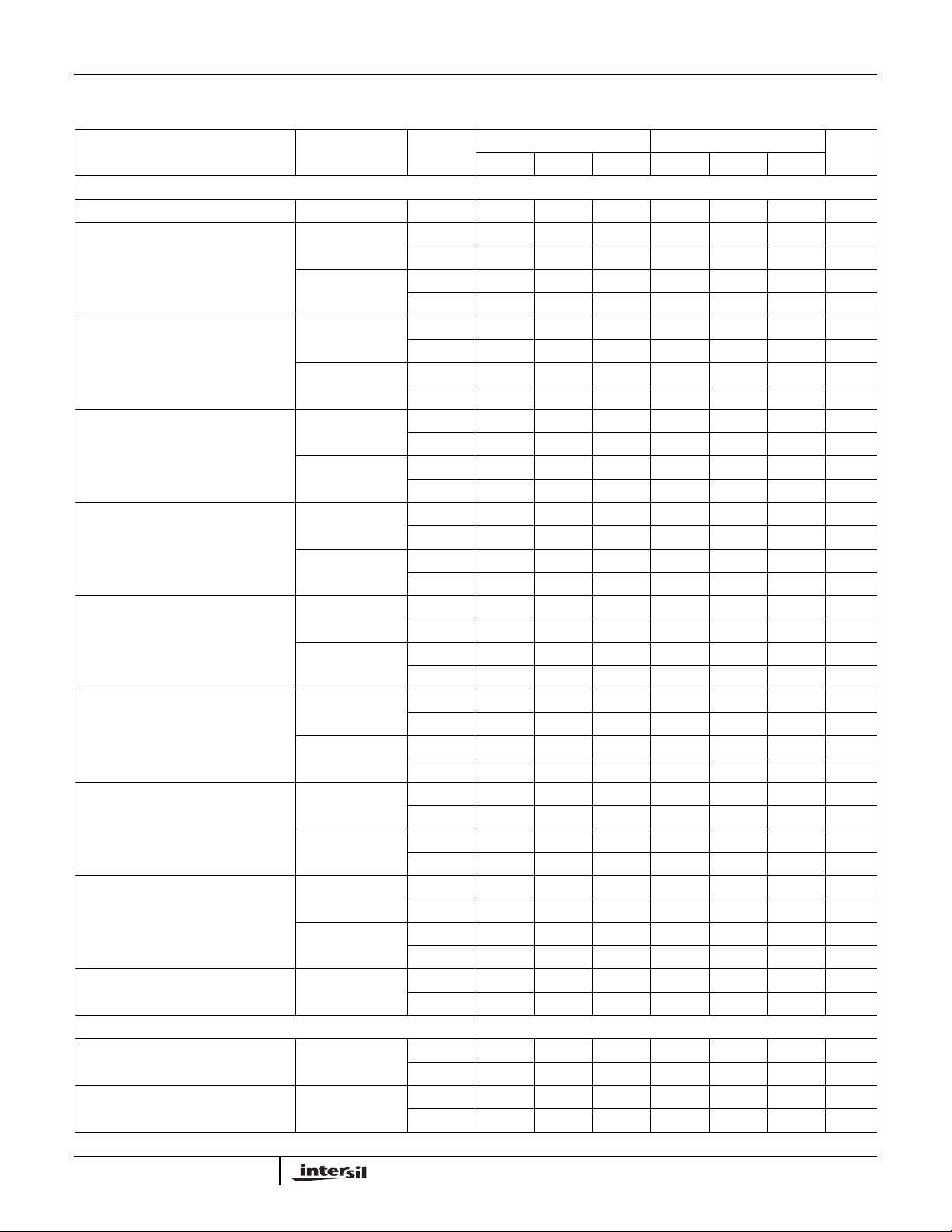
ANALOG CHANNEL CHARACTERISTICS
Analog Signal Range, V
On Resistance, r
ON
IN
VIN = 0V 25 - 650 850 - 650 850 Ω
Full -10 - +10 -10 - +10 V
Full - 950 1.3K - 800 1K Ω
VlN = ±10V 25 - 700 900 - 700 900 Ω
Full - 1.1K 1.4K - 900 1.1K Ω
∆r
(Side A-Side B) VIN = 0V 25 - 4.0 24 - 4.0 24 Ω
ON,
Full - 4.75 28 - 4.0 24 Ω
VlN = ±10V 25 - 4.5 27 - 4.5 27 Ω
Full - 5.5 33 - 4.5 27 Ω
Off Input Leakage Current, I
∆I
(Side A-Side B) Condition 0V 25 - 3 - - 3 - pA
S(OFF),
S(OFF)
Condition 0V
(Note 2)
Condition ±10V
(Note 2)
25 -30- -30-pA
Full - 2 10 - 0.2 1 nA
25 - 100 - - 100 - pA
Full - 5 25 - 0.5 2.5 nA
Full - 0.2 2 - 0.02 0.2 nA
Condition ±10V 25 - 10 - - 10 - pA
Full - 0.5 5 - 0.05 0.5 nA
Off Output Leakage Current,
I
D(OFF)
∆I
(Side A-Side B) Condition 0V 25 - 3 - - 3 - pA
D(OFF),
Condition 0V
(Note 2)
Condition ±10V
(Note 2)
25 -30- -30-pA
Full - 2 10 - 0.2 1 nA
25 - 100 - - 100 - pA
Full - 5 25 - 0.5 2.5 nA
Full - 0.2 2 - 0.02 0.2 nA
Condition ±10V 25 - 10 - - 10 - pA
Full - 0.5 5 - 0.05 0.5 nA
On Channel Leakage Current, I
∆I
(Side A-Side B) Condition 0V 25 - 10 - - 10 - pA
D(ON),
D(ON)
Condition 0V
(Note 2)
Condition ±10V
(Note 2)
25 -50- -50-pA
Full - 5 25 - 0.5 2.5 nA
25 - 150 - - 150 - pA
Full - 6 40 - 0.8 4.0 nA
Full - 0.5 5 - 0.05 0.5 nA
Condition ±10V 25 - 30 - - 30 - pA
Full - 0.6 6 - 0.08 0.8 nA
Differential Offset Voltage, ∆V
OS
Note 3 25 - 0.02 - - 0.02 - µV
Full - 0.70 - - 0.08 - µV
POWER SUPPLY CHARACTERISTICS
Power Dissipation, P
D
25 - 2.3 - - 2.3 - mW
Full - - 45 - - 45 mW
Current, l+ 25 - 0.150 - - 0.150 - mA
Full - - 2.0 - - 2.0 mA
3

HI-539
Electrical Specifications Supplies = ±15V, V
= 4V, VAH (Logic Level High) = 4V, VAL (Logic Level Low) = 0.8V,
EN
Unless Otherwise Specified (Continued)
-8 -5
UNITSMIN TYP MAX MIN TYP MAX
PARAMETER
TEST
CONDITIONS
TEMP
(oC)
Current, l- 25 - 0.001 - - 0.001 - mA
Full - - 1.0 - - 1.0 mA
Supply Voltage Range Full ±5 ±15 ±18 ±5 ±15 ±18 V
NOTES:
2. See Figures 2B, 2C, 2D. The condition ±10V means:
l
S(OFF)
and I
D(OFF)
:
(VS = +10V, VD = -10V), then
(VS = -10V, VD = +10V)
I
: (+10V, then -10V)
D(ON)
3. ∆VOS(Exclusive of thermocouple effects) = rON∆I
4. VlN = 1kHz, 15V
on all but the selected channel. See Figure 7.
P-P
D(ON)
+ I
D(ON)∆rON
. See Applications section for discussion of additional VOS error.
5. Calculated from typical Single-Ended Crosstalk performance.
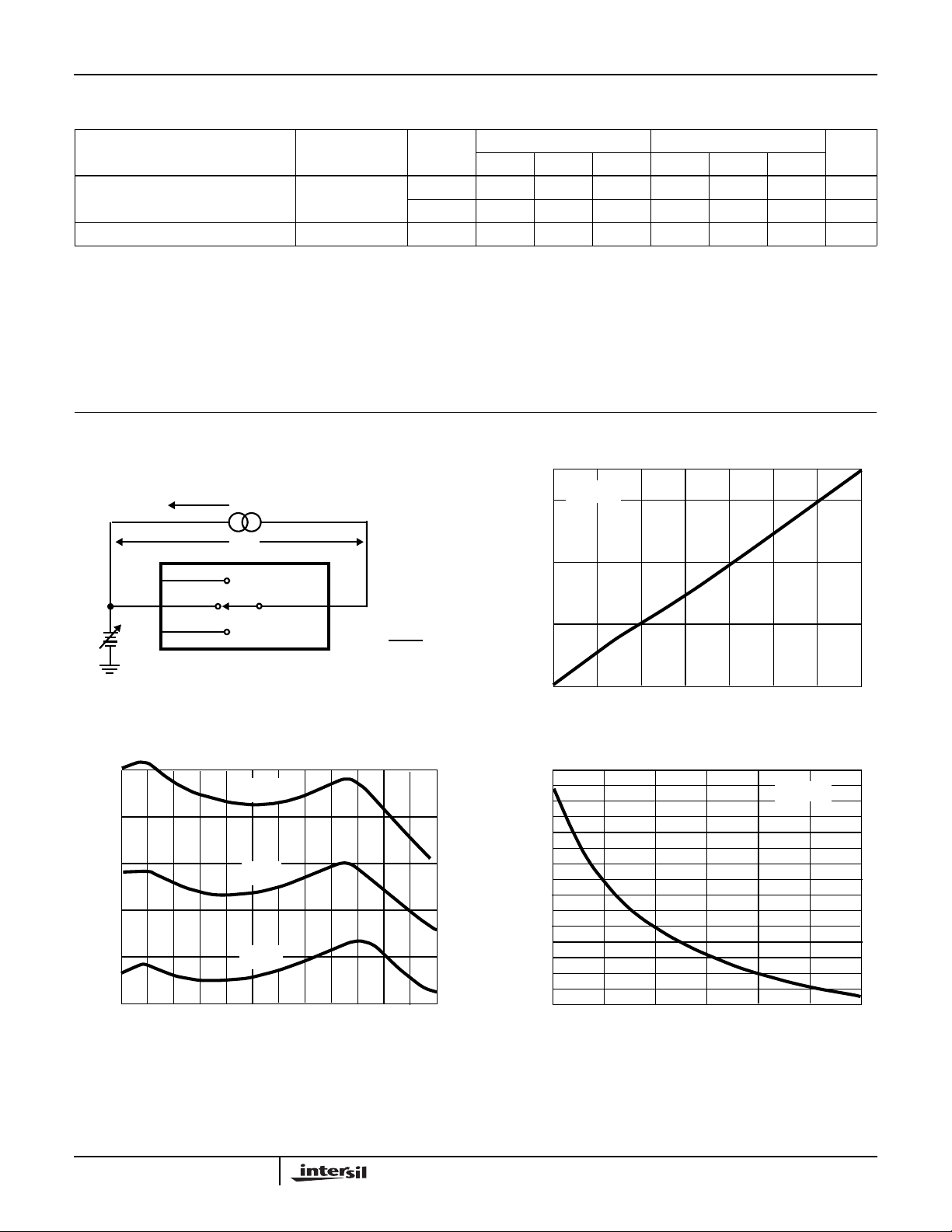
T est Cir cuits and Waveforms
100µA
V
2
Unless Otherwise Specified TA = 25oC, V+ = +15V, V - = -15V, VAH = 4V and VAL = 0.8V
VIN = 0V
800
700
OUTIN
V
V
IN
HI-539
rON =
2
100µA
600
ON RESISTANCE (Ω)
500
-25 0 25 50 75 100 125
-50
TEMPERATURE (
o
C)
FIGURE 1A. TEST CIRCUIT FIGURE 1B. ON RESISTANCE vs TEMPERATURE
900
125oC
800
700
600
ON RESISTANCE (Ω)
500
400
-12
-10 -8 -6 -4 -2 0 2 4 8 10612
25oC
-55oC
ANALOG INPUT (V)
2.0
1.9
1.8
1.7
1.6
1.5
1.4
1.3
1.2
1.1
1.0
ON RESISTANCE (kΩ)
0.9
0.8
0.7
0.6
0.5
5 7 9 11 13 15 17
SUPPLY VOLTAGE (±V)
VIN = 0V
FIGURE 1C. ON RESISTANCE vs ANALOG INPUT VOLTAGE FIGURE 1D. ON RESISTANCE vs SUPPLY VOLTAGE
FIGURE 1. ON RESISTANCE
4
 Loading...