Intersil Corporation HI2325 Datasheet

TM
HI2325
Data Sheet March 2000
3.3V Dual 8-Bit, 40MSPS A/D Converter
with Internal Reference and Digital Clamp
The HI2325 is a monolithic, dual 8-bit, 40MSPS analog-todigital converter fabricated in an advanced CMOS process.
It is designed for high speed applications where integration,
bandwidth and accuracy are essential. The HI2325 features
a 2-stage parallel architecture. Only one external clock is
necessary to drive both converters and an internal voltage
referenceis provided allowing the system designer to realize
an increased level of system integration resulting in
decreased cost and power dissipation.
The HI2325 has excellent dynamic performance while
consuming less than 100mW power at 40MSPS. The A/D
only requires a single +3.3V power supply and encode clock.
Data output latches are provided which present valid data to
the output bus with a latency of 2 clock cycles.
Ordering Information
PART
NUMBER
HI2325IN -20 to 85 48 Ld MQFP/PQFP Q48.7x7-S
TEMP.
RANGE (oC) PACKAGE PKG. NO.
File Number 4823.1
Features
• Sampling Rate . . . . . . . . . . . . . . . . . . . . . . . . . . .40MSPS
• 6.5 Bits at f
= 1MHz
IN
• Low Power at 40MSPS. . . . . . . . . . . . . . . . . . . . . 100mW
• Power Down Mode . . . . . . . . . . . . . . . . . . . . . . . . . . 8mW
• Wide Full Power Input Bandwidth. . . . . . . . . . . . . 250MHz
• Excellent Channel-to-Channel Isolation. . . . . . . . . >75dB
• Internal Digital Clamp
• Internal Voltage Reference
• Single Supply Voltage Operation . . . . . . . . . . . . . . . +3.3V
• TTL/CMOS Compatible Digital Inputs
• CMOS Compatible Digital Outputs. . . . . . . . . . . . . . . 3.3V
• Offset Binary or 2’s Complement Output Format
• Dual 8-Bit A/D Converters on a Monolithic Chip
Applications
• Wireless Local Loop
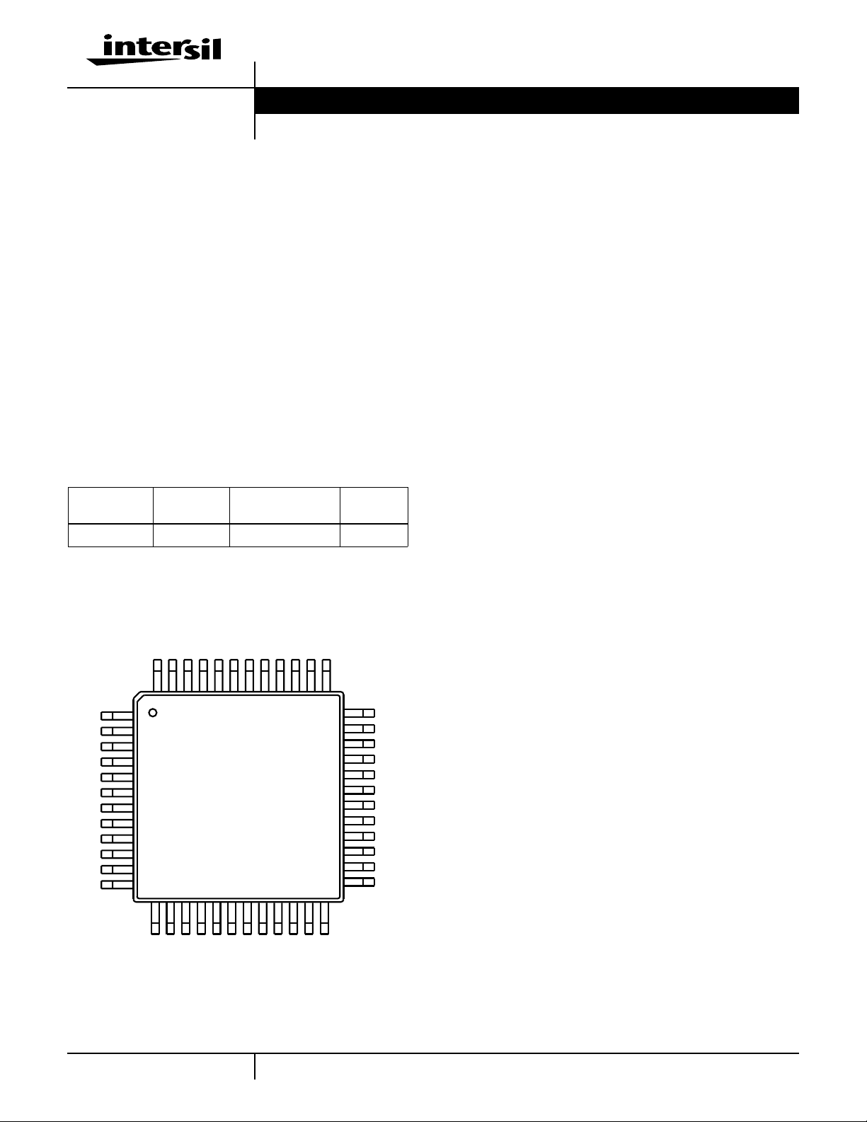
Pinout
A3
A4
A5
A6
A7
DVDD
DVDD
B0
B1
B2
B3
B4
A1
A2
1
2
3
4
5
6
7
8
9
10
11
12
13 14 15 16
B6
B5
48 LEAD LQFP
TOP VIEW
A0
B7
DVSS
DVSS
CLK
2S/B
CLP
REF0
CLE
REF1
REF2
SEL
STB
TEST
AVSS
AVDD
ARBS
373839404142434445464748
36
35
34
33
32
31
30
29
28
27
26
25
2423222120191817
BRB
BRBS
ARB
• PSK and QAM I&Q Demodulators
• Medical Imaging and Instrumentation
• Portable Communications
• Power Metering
• Hand-Held Data Collection Instruments
AVSS
AIO
AIN
AVDD
ART
ARTS
BRTS
BRT
AVDD
BIN
BIO
AVSS
1
1-888-INTERSIL or 321-724-7143 | Intersil and Design is a trademark of Intersil Corporation. | Copyright © Intersil Corporation 2000
CAUTION: These devices are sensitive to electrostatic discharge; follow proper IC Handling Procedures.

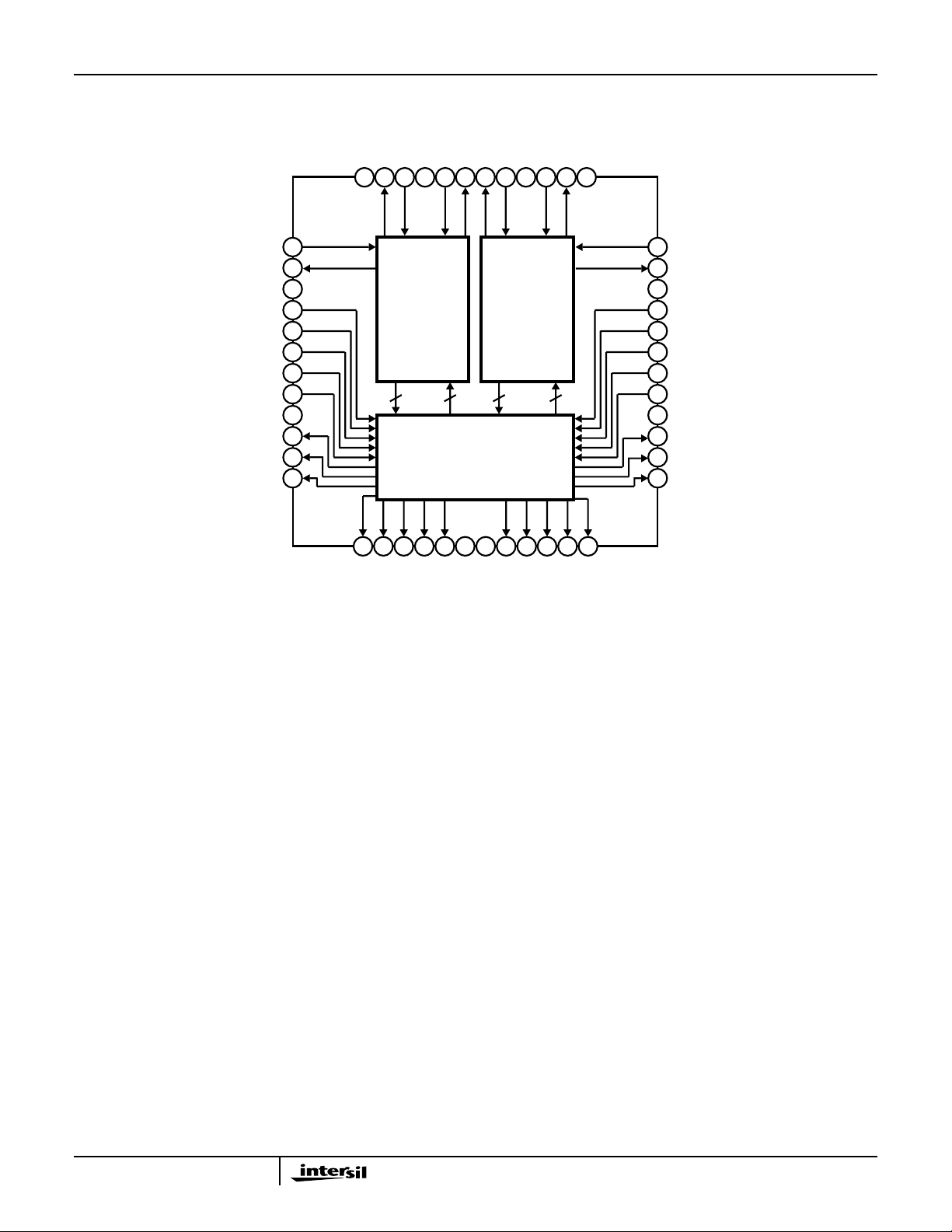
Functional Block Diagram
HI2325
A
RB
A
RBS
AVDD
STB
SEL
CLE
CLP
CLK
DVSS
A0
A1
A2
SS
AV
36 35 34 33 32 31 30 29 28 27 26 25
37
38
39
40
41
42
43
44
45
46
47
48
1 2 3 4 5 6 7 8
A3
DD
ARTS
AV
AIO
8-BIT ADC
88
A4
ART
AIN
A-CH
AND
99
CLAMP AND LATCH
AND TEST
A7
A6
A5
DVDD
BRITS
BRT
B-CH
8-BIT ADC
AND
CLAMP DACCLAMP DAC
B0
DVDD
DD
AV
BIO
BIN
9 11 12
10
B3
B1
B2
AV
SS
B4
BRB
24
BRBS
23
AVSS
22
TEST
21
REF2
20
REF1
19
REF0
18
2S/B
17
DVSS
16
B7
15
B6
14
B5
13
2

HI2325
Pin Descriptions
PIN NO. SYMBOL I/O EQUIVALENT CIRCUIT DESCRIPTION
46, 47, 48,1-5 A0 - A7 O Digital Output. A0(LSB) - A7(MSB)
8 - 15 B0 - B7 O Digital Output. B0(LSB) - B7(MSB)
6, 7 DVDD Digital power supply.
16 DVSS Digital ground.
17 2S/B I Pull-down resistors are
incorporated.
18, 19, 20 REF0 ~ 2 I Pull-down resistors are
incorporated.
21 TEST I Pull-down resistors are
incorporated.
22, 25 DVSS Digital ground.
22, 25, 36 AVSS Analog ground.
23
38
24
37
29
32
30
31
26
35
27
34
28, 33, 39 AVDD Analog power supply.
BRBS
ARBS
BRB
ARB
BRT
ART
BRTS
ARTS
BIO
AIO
BIN
AIN
O Analog output. The digital clamp circuit comprises a D/A converter
I Analog input.
Selects output code.
H: 2’s Compliment Code L: Binary Code
Determines the clamp circuit reference data. See the table “Digital
Clamp Reference Level”.
Normally open.
Shorting these pins to AVSS generates voltage of about 0.5V at the
BRB and ARB pins.
Reference voltage (bottom).
Reference voltage (top).
Shorting these pins to AVDD generates voltage of about 2.5V at the
BRT and ART pins.
whose outputs are available on these pins.
40 STB I Pull-down resistors are
incorporated.
41 SEL I Pull-down resistors are
incorporated.
42 CLE I Pull-down resistors are
incorporated.
43 CLP I Pull-down resistors are
incorporated.
44 CLK I Pull-down resistors are
incorporated.
3
Stand-by input.
H: Stand-by mode L: Operation mode.
Controls the CLP signal polarity.
H: CLP is High active L: CLP is Low active.
Clamp enable input.
H: Enable L: Disable.
Clamp pulse input. The polarity can be set to either High or Low by
setting SEL.
Clock input.
 Loading...