Intersil Corporation HI20206 Datasheet

Semiconductor
HI20206
See HI1178
August 1997
NOT RECOMMENDED FOR NEW DESIGNS
Features
• Resolution . . . . . . . . . . . . . . . . . . . . . . . . . . .Triple 8-Bit
• Maximum Conversion Speed . . . . . . . . . . . . . . . 35MHz
• RGB 3-Channel Input/Output
• Differential Linearity Error . . . . . . . . . . . . . . . ±
1
• Digital Input Voltage . . . . . . . . . . . . . . . . . . . .TTL Level
• Output Voltage Full-Scale . . . . . . . . . . . . . . 1V
P-P
• Low Power Consumption . . . . . . . . . . . . . 360mW (Typ)
• +5V Single Power Supply
• Direct Replacement for Sony CX20206
Applications
• Digital TV
• Graphics Display
• High Resolution Color Graphics
• Video Reconstruction
• Instrumentation
• Image Processing
• I/Q Modulation
/2 LSB
(Typ)
Triple 8-Bit, 35 MSPS, RGB,
3-Channel D/A Converter
Description
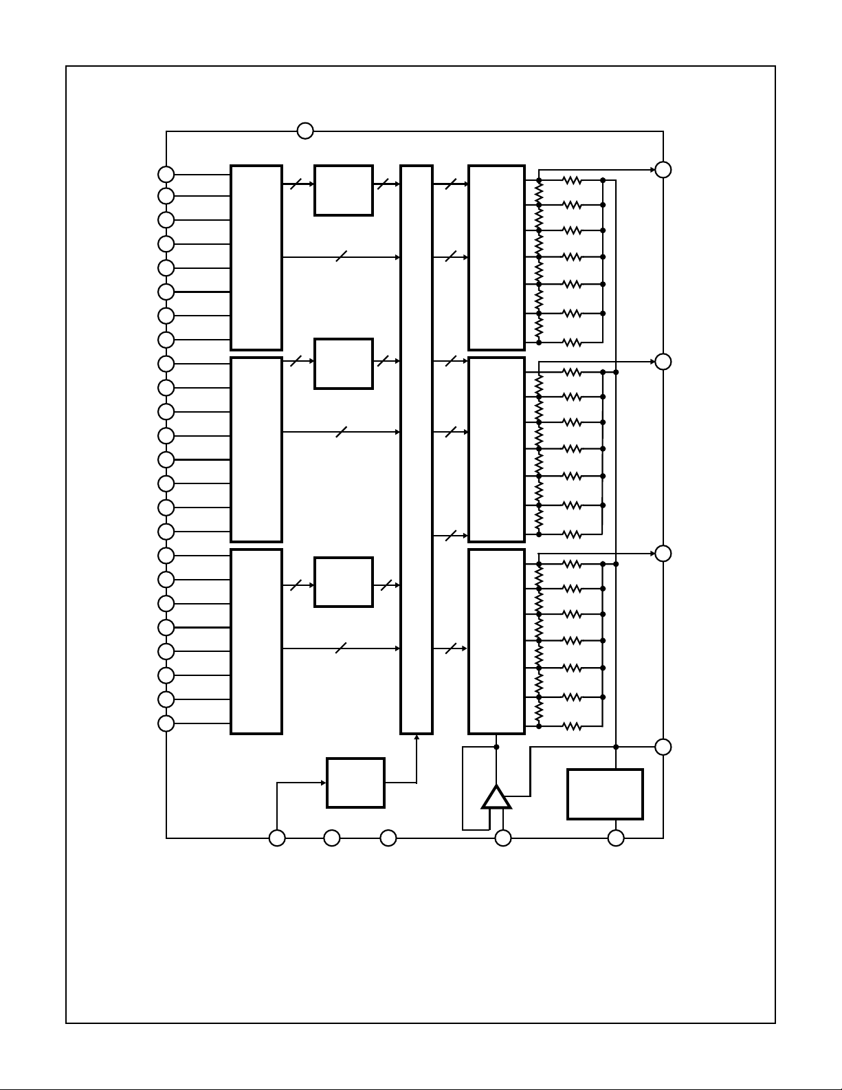
The HI20206 is a triple 8-bit, high-speed, bipolar D/A
converter designed for video band use. It has three separate, 8-bit pixel inputs, one each for red, green, and blue
video data. A single 5.0V power supply and pixel clock input
is all that is required to make the device operational. A bias
voltage generator is internal. For lower CMOS power
consumption, refer to the HI1178.
Ordering Information
TEMP.
PART NUMBER
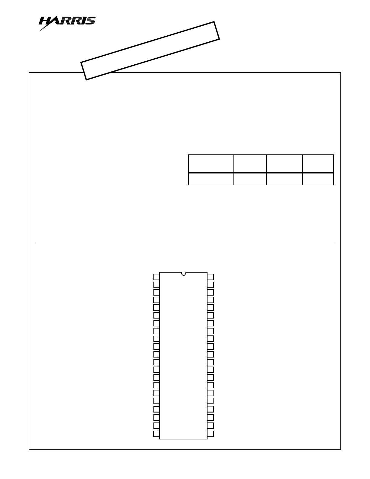
HI20206JCP -20 to 75 42 Ld PDIP E42.6B-S
RANGE (oC) PACKAGE PKG. NO.
Pinout
HI20206 (PDIP)
TOP VIEW
1
R5
R6
2
R7
3
R8
4
G1
5
G2
6
G3
7
G4
8
G5
9
G6
10
G7
11
G8
12
B1
13
B2
14
B3
15
B4
16
B5
17
B6
18
B7
19
B8
20
21CLK 22 DV
42
R4
41
R3
40
R2
39
R1
38
NC
37
DGND
36
NC
35
ROUT
34
NC
33
GOUT
32
NC
31
BOUT
30
NC
AV
29
CC
28
NC
27
V
SET
26
V
REF
25
AGND
24
NC
23
NC
CC
CAUTION: These devices are sensitive to electrostatic discharge. Users should follow proper IC Handling Procedures.
Copyright
© Harris Corporation 1997
10-1
File Number 4111.1

Functional Block Diagram
39
R1
40
R2
41
R3
42
R4
R5
R6
R7
R8
G1
G2
G3
G4
G6
G7
G8
B1
B2
B3
1
2
3
4
5
6
7
8
9G5
10
11
12
13
14
15
INPUT
BUFFER
(R)
INPUT
BUFFER
(G)
HI20206
DGND
37
DECODER
23
6
DECODER
23
6 6
DECODER
23
3
6
3
CLOCK SYNCHRONIZING CIRCUIT
3
CURRENT
SWITCH
(R)
CURRENT
SWITCH
(G)
ROUT
33
RR
2RR
R
2R
R
2R
R
2R
R
2R
R
RR
2RR
R
2R
R
2R
R
2R
R
2R
R
RR
2RR
33
31
GOUT
BOUT
B4
B5
B6
B7
B8
16
17
18
19
20
INPUT
BUFFER
(B)
CLOCK
BUFFER
21 22 23 26
CLK
CC
AGNDDV
66
CURRENT
SWITCH
(B)
V
RET
R
2R
R
2R
R
2R
R
2R
R
INTERNAL
REFERENCE
VOLTAGE
+-
SOURCE
27
V
REF
AV
29
CC
10-2

HI20206
Pin Descriptions
PIN NO. SYMBOL EQUIVALENT CIRCUIT DESCRIPTION
1 To 20
39 To 42
R1 To R8
G1 To G8
B1 To B8
DV
CC
22
39 - 42
1 ~ 20
37
DGND
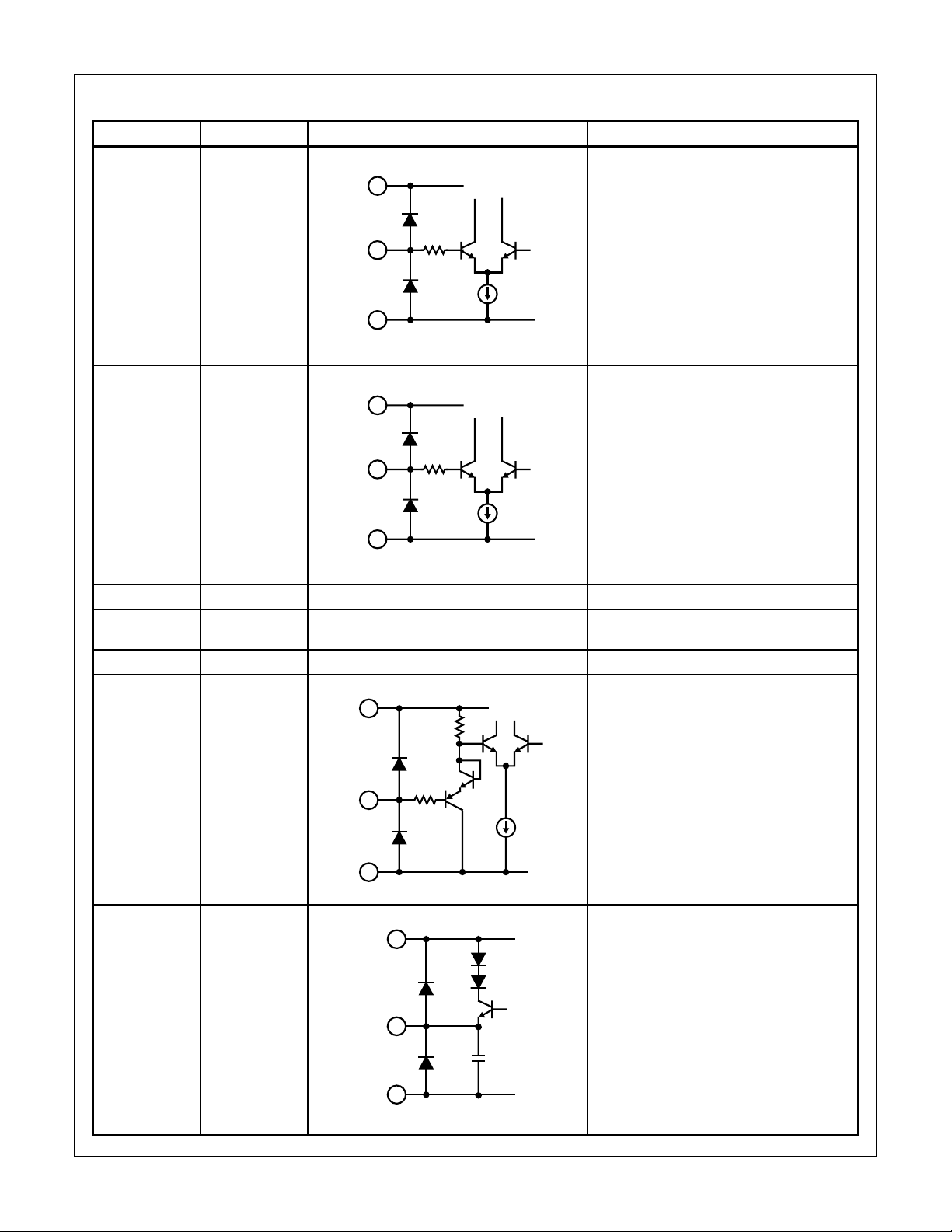
Digital Input pin. From pins 39 to 42 and from 1
to 4 are for RED. R1 is MSB and R8 is LSB.
From pins 5 to 12 are for GREEN. G1 is MSB
and G8 is LSB. From pins 13 to 20 are for
BLUE. B1 is MSB and B8 is LSB.
21 CLK Clock Input pin.
22 DV
23
CC
NC No Connect.
DV
CC
22
21
37
DGND
Digital VCC.
24
25 AGND Analog GND.
26 V
SET
AV
CC
29
54K
26
Bias Input pin. Normally, apply 0.8V.
27 V
REF
25
AGND
AV
CC
29
27
25
AGND
Internal Reference Voltage Output pin 1.2V
(Typ). A pulldown resistance is necessary
externally.
20P
10-3

HI20206
Pin Descriptions
(Continued)
PIN NO. SYMBOL EQUIVALENT CIRCUIT DESCRIPTION
28 NC No Connect.
29 AV
CC
Analog VCC.
30 NC Vacant pin but connect to AVCC (Note 1).
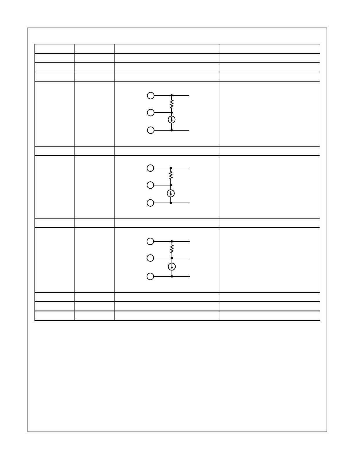
31 BOUT Analog Output pin for BLUE.
AV
CC
29
31
25
AGND
R
O
32 NC Vacant pin but connect to AV
33 GOUT Analog Output pin for GREEN.
AV
CC
29
33
25
AGND
R
O
(Note 1).
CC
34 NC Vacant pin but connect to AVCC (Note 1).
35 ROUT Analog Output pin for RED.
36 NC Vacant pin but connect to AV
AV
CC
29
35
25
AGND
R
O
(Note 1).
CC
37 DGND Digital GND.
38 NC No Connect.
NOTE:
1. Pins 30, 32, 34 and 36 are vacant, but in order to reduce interference between the individual RGB outputs, connect them to AVCC.
10-4
 Loading...