


®
www.BDTIC.com/Intersil
HI-200/883
Data Sheet January 30, 2006
Dual SPST CMOS Analog Switch
The HI-200/883 is a monolithic device comprising two
independently selectable SPST switchers which feature fast
switching speeds (240ns typical) combined with low power
dissipation (15mW typical @ +25°C).
Each switch provides low “ON” resistance operation for input
signal voltages up to the supply rails and for signal currents
up to 25mA continuous. Rugged DI construction eliminates
latch-up and substrate SCR failure modes.
All devices provide break-before-make switching and are
TTL and CMOS compatible for maximum application
versatility. HI-200/883 is an ideal component for use in high
frequency analog switching. Typical applications include
signal path switching, sample and hold circuits, digital filters,
and op amp gain switching networks.
Functional Diagram
LOGIC
INPUT
V+ V
REFERENCE,
LEVEL SHIFTER,
AND DRIVER
V-
REF
GATE
SOURCE
SWITCH
CELL
INPUT
GATE
DRAIN
OUTPUT
FN6059.2
Features
• This Circuit is Processed in Accordance to MIL-STD-883
and is Fully Conformant Under the Provisions of
Paragraph 1.2.1.
• Low “On” Release . . . . . . . . . . . . . . . . . . . . . . .100Ω Max
• Wide Analog Signal Range . . . . . . . . . . . . . . . . . . . .±15V
• TTL/CMOS Compatible . . . . . . . . . . . . . . 2.4V (Logic “1”)
• Turn-On Time . . . . . . . . . . . . . . . . . . . . . . . . . . . . . .500ns
• Analog Current Range (Continuous) . . . . . . . . . . . . 25mA
• No Latch-Up
• Replaces DG200
Applications
• High Frequency Analog Switching
• Sample and Hold Circuits
• Digital Filters
• Op Amp Gain Switching Networks
Ordering Information
TEMP.
PART NUMBER
HI2-0200/883 -55 to 125 10 Pin Metal Can T10.B
RANGE (°C) PACKAGE
PKG.
DWG. #
Pinout
HI2-200/883 (METAL CAN)
TOP VIEW
V+
A
1
10
1
IN1
9
1
CAUTION: These devices are sensitive to electrostatic discharge; follow proper IC Handling Procedures.
1-888-INTERSIL or 1-888-468-3774
| Intersil (and design) is a registered trademark of Intersil Americas Inc.
All other trademarks mentioned are the property of their respective owners.
A
2
2
3
GND
4
IN2
Copyright Intersil Americas Inc. 2004, 2006. All Rights Reserved
5
OUT2
OUT1
8
7
V
REF
6
V-
HI-200/883
www.BDTIC.com/Intersil
Absolute Maximum Ratings Thermal Information
Voltage Between V+ and V- Terminals . . . . . . . . . . . . . . . . . . . .40V
±V
Analog Input Voltage, (+V
Analog Input Voltage, (-V
Digital Input Voltage, (+V
Digital Input Voltage, (-V
to Ground (V+, V-) . . . . . . . . . . . . . . . . . . . . . . . . . . . . ±20V
SUPPLY
) . . . . . . . . . . . . . . . . . . +V
S
). . . . . . . . . . . . . . . . . . . . -V
S
) . . . . . . . . . . . . . . . . . . . +V
A
). . . . . . . . . . . . . . . . . . . . . -V
A
SUPPLY
SUPPLY
SUPPLY
SUPPLY
+2V
-2V
+4V
-4V
Thermal Resistance θ
Metal Can Package . . . . . . . . . . . . . . . 160 75
Package Power Dissipation at +75°C
Metal Can Package . . . . . . . . . . . . . . . . . . . . . . . . . . . . 0.62W/°C
Package Power Dissipation Derating Factor above +75°C
Metal Can Package . . . . . . . . . . . . . . . . . . . . . . . . . . .8.24mW/°C
Peak Current (S or D)
(Pulse at 1ms, 10% Duty Cycle Max). . . . . . . . . . . . . . . . . . 40mA
Continuous Current . . . . . . . . . . . . . . . . . . . . . . . . . . . . . . . . . 25mA
Junction Temperature . . . . . . . . . . . . . . . . . . . . . . . . . . . . . .+175°C
Storage Temperature Range. . . . . . . . . . . . . . . . . .-65°C to +150°C
Lead Temperature (Soldering 10s) . . . . . . . . . . . . . . . . . . . . . . ≤275°C
CAUTION: Stresses above those listed in “Absolute Maximum Ratings” may cause permanent damage to the device. This is a stress only rating and operation of the
device at these or any other conditions above those indicated in the operational sections of this specification is not implied.
Recommended Operating Conditions
Operating Temperature Range . . . . . . . . . . . . . . . .- 55°C to +125°C
Operating Supply Voltage Range (±V
Analog Input Voltage (V
Logic Low Level (VAL). . . . . . . . . . . . . . . . . . . . . . . . . . . 0V to 0.8V
Logic High Level (V
) . . . . . . . . . . . . . . . . . . . . . . . . ±V
S
) . . . . . . . . . . . . . . . . . . . . 2.4V to +V
AH
SUPPLY
(°C/W) θJC (°C/W)
JA
). . . . . . . . . . . . . . ±15V
SUPPLY
SUPPLY
Device Tested at: +V
SUPPLY
= +15V, −V
SUPPLY
= −15V, V
D.C. PARAMETERS SYMBOL CONDITIONS
TABLE 1. D.C. ELECTRICAL PERFORMANCE SPECIFICATIONS
Switch
“ON” Resistance r
VA = 0.8V, VS = 10V, ID = -1mA,
DS
All Unused Channels V
= 0.8V, VS = -10V, ID = 1mA,
V
A
All Unused Channels V
Source “OFF”
Leakage Current
Drain “OFF”
Leakage Current
Channel “ON”
Leakage Current
I
S(OFF)VS
I
D(OFF)VD
I
D(ON)VD
= +14V, VD = -14V, VA = 2.4V,
All Unused Channels V
= +14V, VS = -14V
V
D
= -14V, VD = +14V, VA = 2.4V,
V
S
All Unused Channels V
= -14V, VS = +14V
V
D
= -14V, VS = +14V, VA = 2.4V,
All Unused Channels V
V
= +14V, VS = -14V
D
= +14V, VS = -14V, VA = 2.4V,
V
D
All Unused Channels V
= -14V, VS = +14V
V
D
= VS = +14V, VA = 0.8V,
All Unused Channels V
= VS = -14V
V
D
= VS = -14V, VA = 0.8V,
V
D
All Unused Channels V
V
= VS = +14V
D
Low Level
Input Current
High Level
Input Current
Supply Current +I
I
I
VAL = 0.8V
AL
All Channels V
VAH = 2.4V
AH
All Channels V
All Channels VA = 0V 1 25 - 2.0 µA
CC
All Channels V
= 2.4V
A
AH
= 3V 1 25 - 2.0 mA
A
= OPEN, GND = 0V, Unless Otherwise Specified.
REF
GROUP A
TEMPERATURE
SUBGROUPS
125-70Ω
= 0.8V
A
2, 3 -55 to 125 - 100 Ω
125-70Ω
= 0.8V
A
2, 3 -55 to 125 - 100 Ω
125-55nA
= 2.4V,
A
2, 3 -55 to 125 -500 500 nA
125-55nA
= 2.4V,
A
2, 3 -55 to 125 -500 500 nA
125-55nA
= 2.4V,
A
2, 3 -55 to 125 -500 500 nA
125-55nA
= 2.4V,
A
2, 3 -55 to 125 -500 500 nA
125-55nA
= 0.8V,
A
2, 3 -55 to 125 -500 500 nA
125-55nA
= 0.8V,
A
2, 3 -55 to 125 -500 500 nA
125-1.01.0µA
2, 3 -55 to 125 -1.0 1.0 µA
125-1.01.0µA
= 4.0V
2, 3 -55 to 125 -1.0 1.0 µA
2, 3 -55 to 125 - 2.0 µA
2, 3 -55 to 125 - 2.0 mA
(°C) MIN MAX UNITS
2
FN6059.2
January 30, 2006
HI-200/883
www.BDTIC.com/Intersil
TABLE 1. D.C. ELECTRICAL PERFORMANCE SPECIFICATIONS (Continued)
Device Tested at: +V
D.C. PARAMETERS SYMBOL CONDITIONS
Supply Current -I
Device Tested at: +V
PARAMETERS SYMBOL CONDITIONS
Turn “ON” Time t
Turn “OFF” Time t
Device Tested at: +V
PARAMETERS SYMBOL CONDITIONS NOTE
Address Capacitance C
Switches Input
Capacitance
Switch Output Capacitance C
Drain to Source
Capacitance
Off Isolation V
Cross Talk V
Charge Transfer Error V
NOTE:
1. Parameters listed in Table 2 are controlled via design or process parameters and are not directly tested at final production. These parameters
are lab characterized upon initial design release, or upon design changes. These parameters are guaranteed by characterization based upon
data from multiple production runs which reflect lot to lot and within lot variation.
SUPPLY
SUPPLY
SUPPLY
= +15V, −V
CC
TABLE 2. A.C. ELECTRICAL PERFORMANCE SPECIFICATIONS
= +15V, −V
ON
OFF
TABLE 3. ELECTRICAL PERFORMANCE SPECIFICATIONS (NOTE 1)
= +15V, −V
A
C
S (OFF)
D (OFF)
C
D (ON)
C
DS
ISO
CT
CTE
= −15V, V
SUPPLY
All Channels VA = 0V 1 25 -2.0 - µA
All Channels V
= −15V, V
SUPPLY
C
= 35pF,
L
R
= 1kΩ
L
C
= 33pF,
L
= 1kΩ
R
L
= −15V, V
SUPPLY
f = 1MHz, VAL = 0V 1 25 - 20 pF
f = 1MHz, VAH = 5V,
Measured Source to GND
f = 1MHz, VAH = 5V,
Measured Output to Ground
f = 1MHz, VAL = 0V,
Measured Output to Ground
f = 1MHz, VAH = 5V 1 25 - 2.0 pF
f = 200kHz, VA = 2.4, RL = 1K,
= 1V
V
GEN
f = 200kHz, VA = 2.4, RL = 1K,
V
= 1V
GEN
f = 200kHz, VA = 0 to 4V,
= 0.01µF
C
L
= OPEN, GND = 0V, Unless Otherwise Specified.
REF
GROUP A
SUBGROUPS
2, 3 -55 to 125 -2.0 - µA
= 3V 1 25 -2.0 - µA
A
2, 3 -55 to 125 -2.0 - µA
= OPEN, GND = 0V, Unless Otherwise Specified.
REF
GROUP A
SUB-
GROUPS
9 25 - 500 ns
10, 11 55 to 125 - 800 ns
9 25 - 500 ns
10, 11 55 to 125 - 650 ns
= OPEN, GND = 0V
REF
1 25 - 20 pF
1 25 - 20 pF
1 25 - 30 pF
12555-dB
= 10pF
P-P, CL
12560-dB
1 25 -10 10 mV
P-P, CL
= 10pF
TEMPERATURE
(°C) MIN MAX UNITS
TEMPERATURE
(°C) MIN MAX UNITS
TEMPERATURE
(°C) MIN MAX UNITS
TABLE 4. ELECTRICAL TEST REQUIREMENTS
MIL-STD-883 TEST REQUIREMENTS SUBGROUPS (Tables 1 and 2)
Interim Electrical Parameters (Pre Burn-in) 1
Final Electrical Test Parameters 1 (Note 2), 2, 3, 9, 10, 11
Group A Test Requirements 1, 2, 3, 9, 10, 11
Groups C & D Endpoints 1
NOTE:
2. PDA applies to Subgroup 1 only.
3
FN6059.2
January 30, 2006
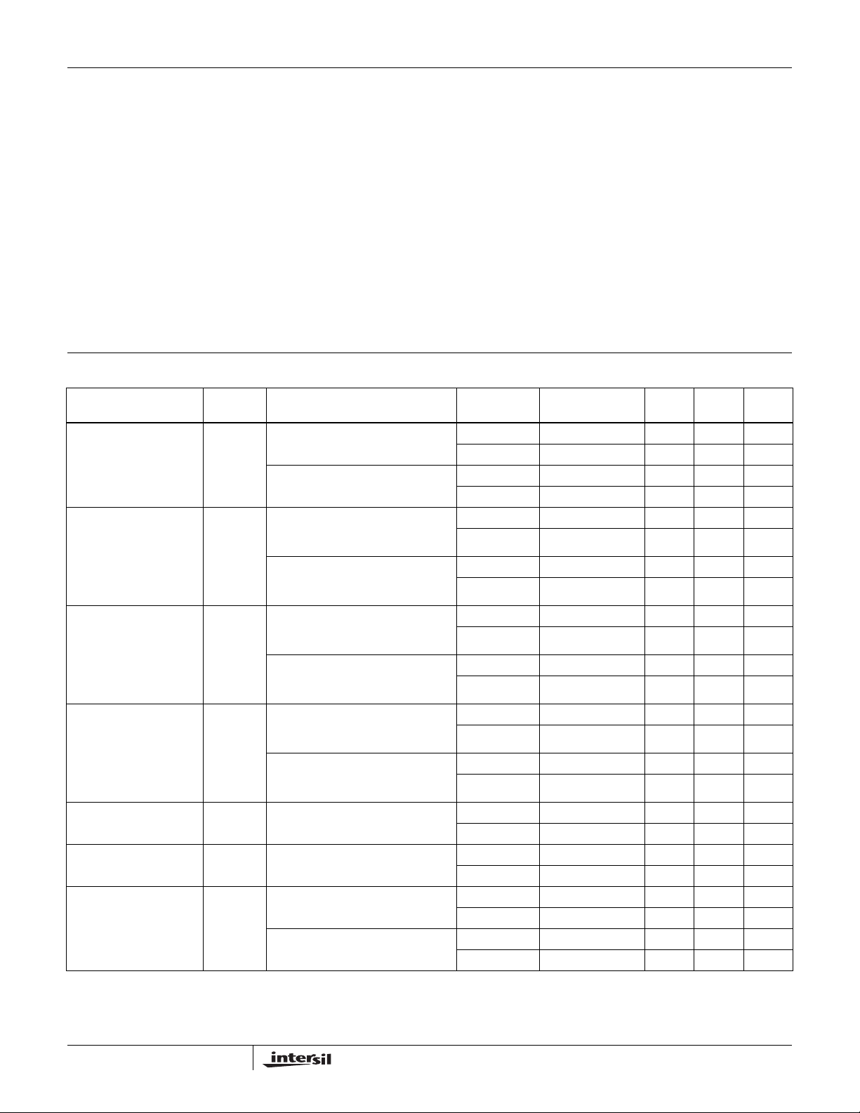
Test Circuits
www.BDTIC.com/Intersil
HI-200/883
+V
CC
S
V
IN
I
IN
-V
GND
CC
D
FIGURE 1. INPUT LEAKAGE CURRENT
+V
CC
V
S
I
S
V
IN
-V
GND
FIGURE 3. IS
CC
(OFF)
S
V
D
S
V
S
V
IN
GND
FIGURE 2. I
V
IN
GND
FIGURE 4. I
+V
CC
D
I
D
-V
CC
V
D
D (OFF)
+V
CC
S
I
D(ON)
D
V
-V
CC
D (ON)
+V
CC
I
1
STEP
S
V
IN
GND
I
2
-V
CC
D
FIGURE 5. SUPPLY CURRENTS
GENERATOR
TEST
POINT
0.01µF
TEST
POINT
0.01µF
FIGURE 6. CHARGE TRANSFER ERROR
15V
V+
IN
1
S
1
D
1
IN
2
S
2
D
2
GNDV-
-15V GND
IN
3
S
3
D
3
IN
4
S
4
D
4
STEP
GENERATOR
(SEE NOTE)
TEST
POINT
0.01µF
TEST
POINT
0.01µF
4
FN6059.2
January 30, 2006

Test Circuits (Continued)
www.BDTIC.com/Intersil
S
V
IN
GND
FIGURE 7. R
+V
HI-200/883
15V
CC
D
V
D
-V
CC
DS
SINE WAVE
GENERATOR
V+
IN
1
S
1
D
1
IN
2
S
2
D
2
GNDV-
-15V GND
IN
3
S
3
D
3
1kΩ
IN
4
2.4V
S
4
D
4
1kΩ
TEST
POINT
TEST
POINT
24V
1kΩ
2.4V
1kΩ
FIGURE 8. OFF CHANNEL ISOLATION
SINE WAVE
GENERATOR
TEST
POINT
TEST
POINT
TEST
POINT
1kΩ
TEST
POINT
1kΩ
0.8V
24V
0.8V
24V
15V
V+
IN
1
S
1
D
1
IN
2
S
2
D
2
GNDV-
-15V GND
24V
IN
3
S
3
D
3
IN
4
S
4
D
4
0.8V
24V
0.8V
1kΩ
TEST
POINT
1kΩ
STEP
GENERATOR
FIGURE 9. CROSSTALK BETWEEN CHANNELS
TEST
POINT
1kΩ
5
FN6059.2
January 30, 2006

Switching Waveforms
www.BDTIC.com/Intersil
HI-200/883
FIGURE 10.
FIGURE 11.
6
FN6059.2
January 30, 2006

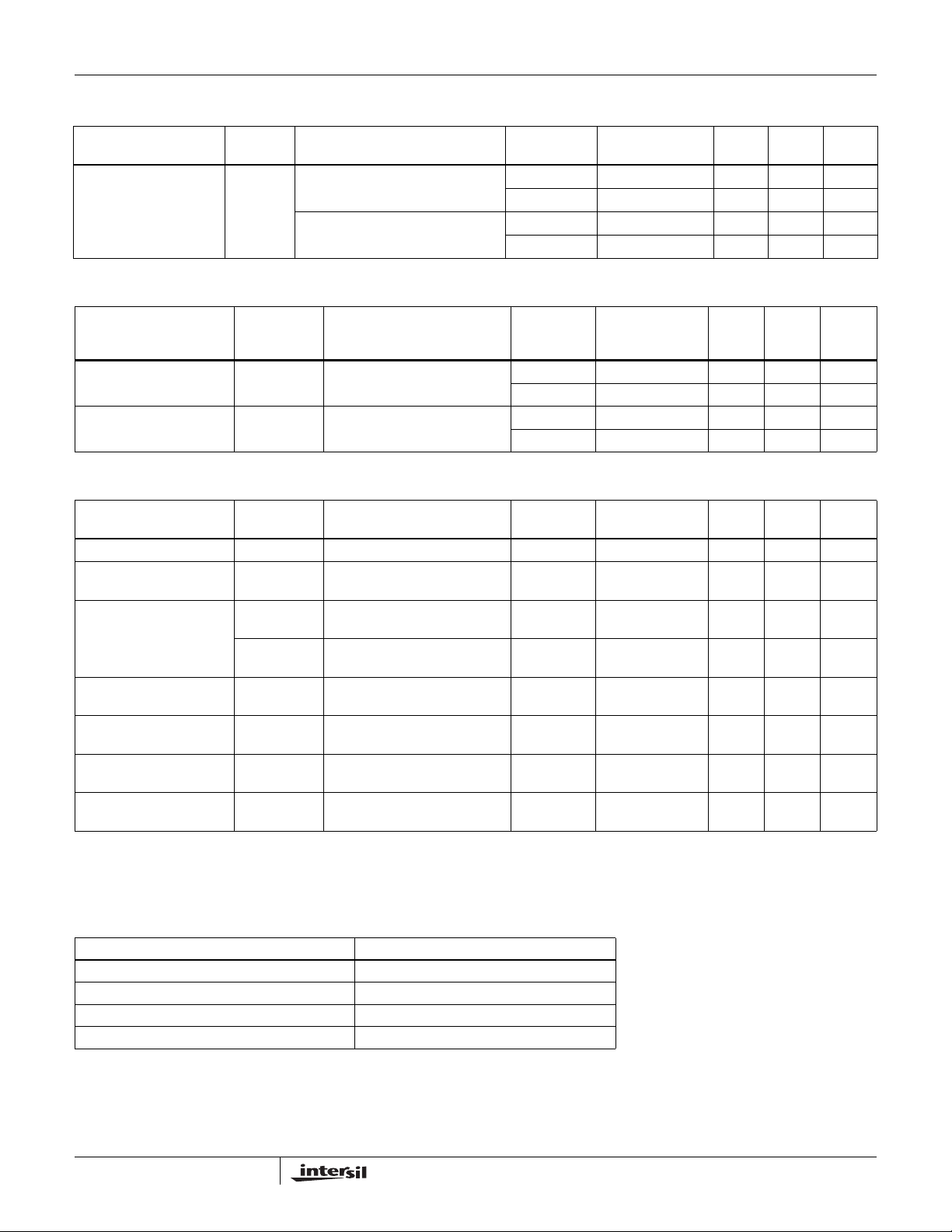
Burn-In Circuit
www.BDTIC.com/Intersil
HI-200/883
NOTES:
3. R1 = R2 = 10kΩ
= C2 = 0.01µF (per socket) or 0.1µF (per row)
4. C
1
= D2 = IN4002 or equivalent
5. D
1
6. |(V+) - (V-)| = 30V
Schematic Diagrams
FIGURE 12. HI-200/883 METAL CAN (TO-99)
TTL/CMOS REFERENCE CIRCUIT V
V+
R
2
GND
V-
5K
D
Q
P1
M
P13
Q
3
Q
N2
N1
R
3
24.2K
R
4
5.4K
R
5
7.9K
Q
P2
Q
P4
M
N15
R
300
M
6
Q
Q
N14
CELL
REF
P3
Q
N4
P5
M
N16
M
N17
V
REF
TO P
V
LL
R
7
100K
2
GND
7
FN6059.2
January 30, 2006

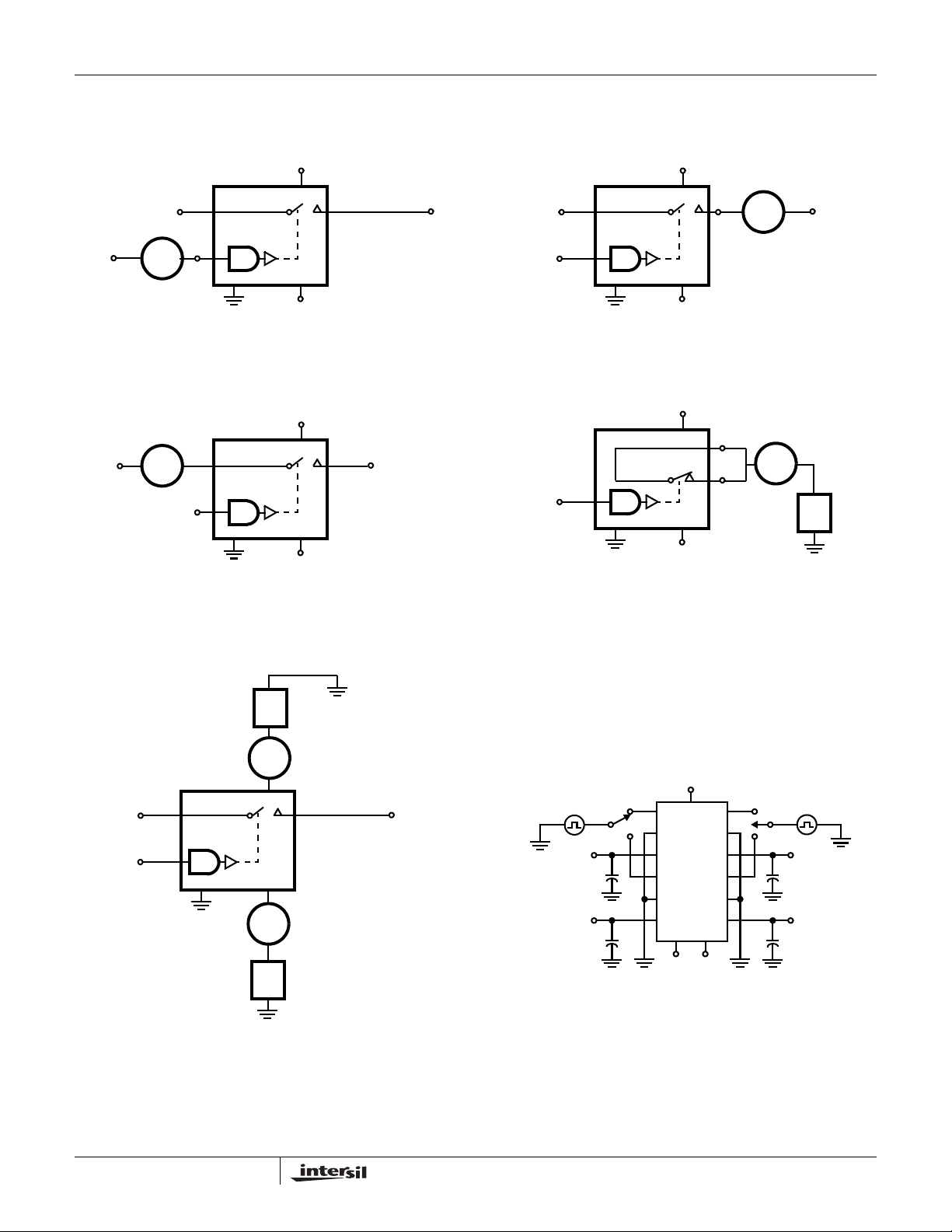
Schematic Diagrams (Continued)
www.BDTIC.com/Intersil
’
A
HI-200/883
SWITCH CELL
N11
P1
P3
INPUT
A’
P4
P11
V+
N13
V-
N12
P12
DIGITAL INPUT BUFFER AND LEVEL SHIFTER
P5
OUTPUT
V+
R
1
200Ω
V+
V-VA
N13
N11
N12
OUTPUT
P12
V-
N1
N8
P8
P9
N9
P7
D
1
D
2
N2
TO V
TO V
P2
LL
REF
N4
N3
P6
N7
N6
N5
V-
N10
P10
INPUT
P11
8
FN6059.2
January 30, 2006

HI-200/883
www.BDTIC.com/Intersil
Test Circuits and Waveforms T
80
70
60
50
40
30
ON RESISTANCE (Ω)
20
10
0
-25-50 0 25 50 75 100 125
TEMPERATURE (°C)
VIN = 0V
= 25°C, V
A
= ±15V, VAH = 2.4V, VAL = 0.8V and V
SUPPLY
100
50
ON RESISTANCE (Ω)
0
-15 -10 -5 0 5 10 15
= Open
REF
V+ = +10V
V- = -10V
V+ = +12.5V
V- = -12.5V
V+ = +15V
V- = -15V
ANALOG SIGNAL LEVEL (V)
FIGURE 13. ON RESISTANCE vs TEMPERATURE FIGURE 14. ON RESISTANCE vs ANALOG SIGNAL
LEVEL AND POWER SUPPLY VOLTAGE
100
I
10
CURRENT (nA)
1.0
0.1
25 50 75 100
S(OFF)/ID(OFF)
I
TEMPERATURE (°C)
D(ON)
125
90
80
70
60
50
40
30
SWITCH CURRENT (mA)
20
10
0
1234 567
0
VOLTAGE ACROSS SWITCH (±V)
FIGURE 15. LEAKA G E CURRENT vs T E MPERATURE FIGURE 16. SWITCH CURRENT vs VOLTAGE
140
120
100
80
60
OFF ISOLATION (dB)
40
20
0
100Hz 1kHz 10kHz 100kHz 1MHz
RL = 1kΩ
FREQUENCY (Hz)
FIGURE 17. OFF ISOLATION vs FREQUENCY
9
January 30, 2006
FN6059.2

Die Characteristics
www.BDTIC.com/Intersil
DIE ATTACH:
Material: Gold/Silicon Eutectic Alloy
Temperature: Metal Can - 420°C (Max)
Metallization Mask Layout
HI-200/883
HI-200
IN 2
GND
3
A
2
A
1
V+
91012
IN 1
8
OUT 2
4 5 6 7
V-
10
V
REF
OUT 1
FN6059.2
January 30, 2006

Metal Can Packages (Can)
www.BDTIC.com/Intersil
HI-200/883
REFERENCE PLANE
A
ØD ØD1
F
Q
Øb1
NOTES:
1. (All leads) Øb applies between L1 and L2. Øb1 applies between
L2 and 0.500 from the reference plane. Diameter is uncontrolled
in L1 and beyond 0.500 from the reference plane.
2. Measured from maximum diameter of the product.
α is the basic spacing from the centerline of the tab to terminal 1
3.
and β is the basic spacing of each lead or lead position (N -1
places) from
4. N is the maximum number of terminal positions.
5. Dimensioning and tolerancing per ANSI Y14.5M - 1982.
6. Controlling dimension: INCH.
α, looking at the bottom of the package.
L
L2
L1
A
A
Øe
Øb1
Øb
BASE AND
SEATING PLANE
BASE METAL LEAD FINISH
SECTION A-A
Øb2
e1
ØD2
2
β
N
1
α
k
T10.B MIL-STD-1835 MACY1-X10 (A2)
10 LEAD METAL CAN PACKAGE
INCHES MILLIMETERS
SYMBOL
A 0.165 0.185 4.19 4.70 -
Øb 0.016 0.019 0.41 0.48 1
k1
C
L
Øb1 0.016 0.021 0.41 0.53 1
Øb2 0.016 0.024 0.41 0.61 -
ØD 0.335 0.375 8.51 9.52 ØD1 0.305 0.335 7.75 8.51 ØD2 0.110 0.160 2.79 4.06 -
e 0.230 BSC 5.84 BSC -
e1 0.115 BSC 2.92 BSC -
F - 0.040 - 1.02 k 0.027 0.034 0.69 0.86 -
k1 0.027 0.045 0.69 1.14 2
L 0.500 0.750 12.70 19.05 1
L1 - 0.050 - 1.27 1
L2 0.250 - 6.35 - 1
Q 0.010 0.045 0.25 1.14 -
α
β 36
N10 104
36o BSC 36o BSC 3
o
BSC 36o BSC 3
NOTESMIN MAX MIN MAX
Rev. 0 5/18/94
All Intersil U.S. products are manufactured, assembled and tested utilizing ISO9000 quality systems.
Intersil Corporation’s quality certifications can be viewed at www.intersil.com/design/quality
Intersil products are sold by description only. Intersil Corporation reserves the right to make changes in circuit design, software and/or specifications at any time without
notice. Accordingly, the reader is ca utioned to verify that data she ets are current before pl acing orders. Information fur nished by Intersil is believed to be accurate and
reliable. However, no responsibility is assumed by Intersil or its subsidiaries for its use; nor for any infringements of patents or other rights of third parties which may result
from its use. No license is granted by implication or othe rwise under any patent or patent rights of Intersil or its subsidia ries.
For information regarding Intersil Corporation and its products, see www.intersil.com
11
FN6059.2
January 30, 2006
 Loading...