Intersil Corporation HI1826 Datasheet

October 1998
Semiconductor
HI1826
See HI3086
NOT RECOMMENDED FOR NEW DESIGNS
6-Bit, 140 MSPS, Flash A/D Converter
Features
• Ultra-High Speed Operation with Maximum
Conversion Rate. . . . . . . . . . . . . . . . . . . . . . . 140 MSPS
[ /Title (HI1826)
• Low Input Capacitance . . . . . . . . . . . . . . . . . . . . . . . 7pF
/Subject (6-Bit, 140 MSPS, Flash A/D Converter)
• Wide Analog Input Bandwidth (Min) . . . . . . . . 200MHz
/Author ()
/Keywords (Harris Semiconductor, RGB, Video, Flat
• Low Power Consumption . . . . . . . . . . . . . . . . . .225mW
Panel, LCD)
• Low Error Rate
/Creator ()
/DOCINFO pdfmark
Applications
• RGB Graphics Processing
[ /PageMode /UseOutlines
• Digital Data Storage Read Channels
/DOCVIEW pdfmark
• Digital Communications
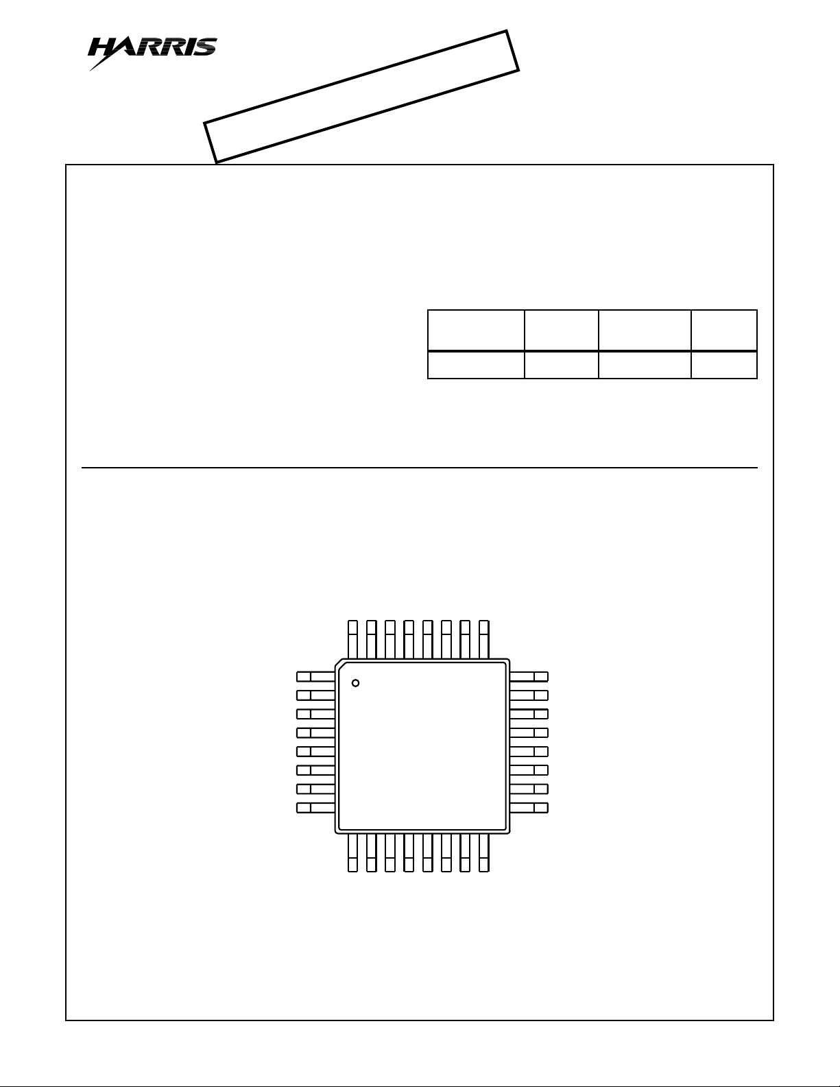
Pinout
HI1826
(MQFP)
TOP VIEW
Description
HI1826 is a 6-bit, 140 MSPS, flash A/D converter IC capable
of digitizing analog signals at the maximum rate of 140
MSPS. The digital input/output level is compatible with the
ECL 100K/10KH/10K.
Ordering Information
PART
NUMBER
HI1826JCQ -20 to 75 32 Ld MQFP Q32.7x7-S
TEMP.
RANGE (oC) PACKAGE PKG. NO.
DGND1
DGND2
NC
NC
NC
NC
DGND2
DGND1
EE
CLKN
CLKP
DV
D0 (LSB)
D1
D2
32 31 30 29 28 27 26 25
1
2
3
4
5
6
7
8
EE
D4
D3
D5 (MSB)
DV
INV
NC
AV
AV
EE
EE
161514131211109
AGND
AGND
24
23
22
21
20
19
18
17
V
RTS
V
RT
AGND
NC
V
IN
AGND
V
RB
V
RBS
CAUTION: These devices are sensitive to electrostatic discharge. Users should follow proper IC Handling Procedures.
Copyright
© Harris Corporation 1998
4-1
File Number 4107.2

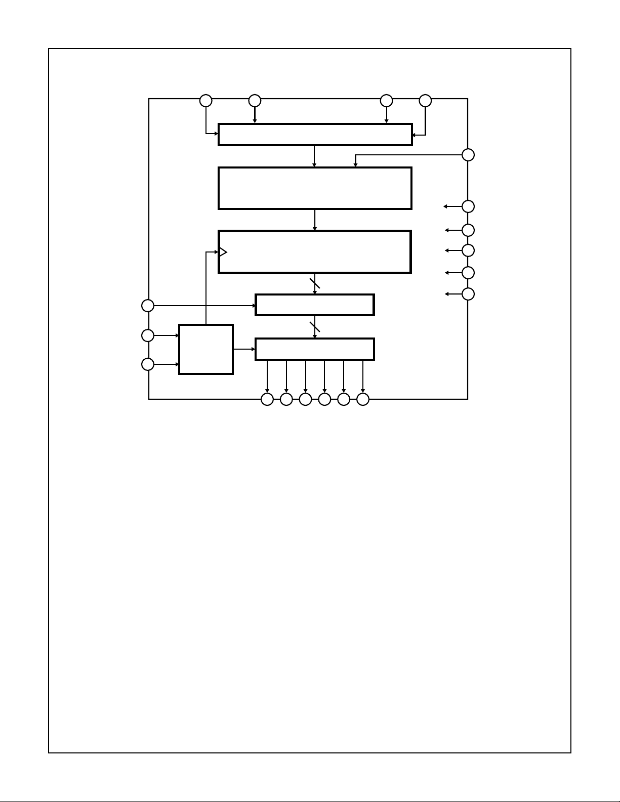
Block Diagram
HI1826
INV
CLKP
CLKN
V
RB
18 17
13
28
CLK DRIVER
27
V
RBS
REFERENCE RESISTANCE
COMPARATOR ARRAY
ENCODER LOGIC
EXOR ARRAY
OUTPUT BUFFER
6
6
V
RTS
24 23
V
RT
20
V
IN
8
DGND1
7
DGND2
19
AGND
12
DV
EE
15
AV
EE
D0
(LSB)
D1
D3 D4 D5
D2
11109323130
(MSB)
4-2

Pin Descriptions
PIN NO. SYMBOL I/O
HI1826
TYPICAL
VOLTAGE
LEVEL EQUIVALENT CIRCUIT DESCRIPTION
16, 19,
22, 25
AGND - 0V Analog GND. Used as GND for input
buffers and latches of comparators.
Separated from DGND1 and DGND2.
15, 26 AV
EE
- -5.2V Analog VEE. Typical voltage is -5.2V.
Connected internally with DVEE.
(Resistance is 4 to 6Ω.) Connect to
AGND through a ceramic chip capacitor
of 0.1µF or more just near the pin.
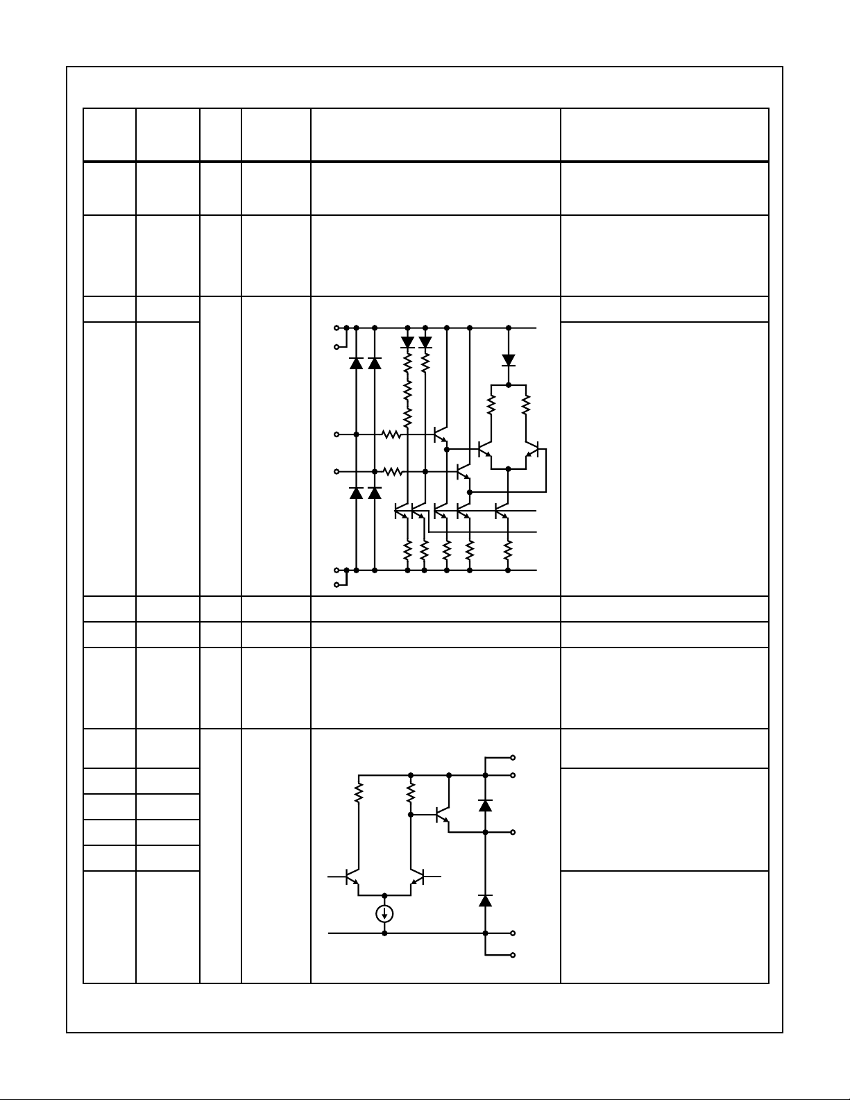
28 CLKP I ECL CLK Input.
DGND1
27 CLKN CLK Complementary Input. When left
R
R
open, voltage goes to ECL threshold
potential (-1.3V). Although only CLKP
input can be used for operation with
R
CLKN input open, complementary input
is recommended in order to attain high
CLKP
CLKN
DV
EE
R
RR
speed and stable operation.
1, 8 DGND1 - 0V Digital GND for Internal Circuits.
2, 7 DGND2 - 0V Digital GND for Output Transistors.
12, 29 DV
EE
- -5.2V Digital VEE. Connected internally with
AVEE. (Resistance is 4 to 6Ω.) Connect
to DGND through a ceramic chip
capacitor of 0.1µF or more just near the
pin.
30 D0 O ECL LSB of Data Output. External pull-down
DGND2
resistor is required.
31 D1 Data Output. External pull-down resistors
are required.
32 D2
9D3
Di
10 D4
11 D5 MSB of Data Output. External pull-down
resistor is required.
DV
EE
4-3
 Loading...