

Intersil Corporation HI1396 Datasheet
HI1396
August 1997
Features
• Differential Linearity Error ±0.5 LSB (Typ) or Less
• Integral Linearity Error ±0.5 LSB (Typ) or Less
• Built-In Integral Linearity Compensation Circuit
• Ultra High Speed Operation with Maximum
Conversion Rate of 125 MSPS (Min)
• Low Input Capacitance (Typ) . . . . . . . . . . . . . . . . .18pF
• Wide Analog Input Bandwidth
(Min for Full Scale Input). . . . . . . . . . . . . . . . . . 200MHz
• Single Power Supply . . . . . . . . . . . . . . . . . . . . . . . .-5.2V
• Low Power Consumption (Typ) . . . . . . . . . . . . .870mW
• Low Error Rate
• Operable at 50% Clock Duty Cycle
• Capable of Driving 50Ω Loads
• Direct Replacement for Sony CXA1396
Applications
• Video Digitizing • Communication Systems
• HDTV (High Definition TV) • Radar Systems
• Direct RF Down-Conversion • Digital Oscilloscopes
8-Bit, 125 MSPS, Flash A/D Converter
Description
The HI1396 is an 8-bit, ultra high speed flash analog-to-digital
converter IC capable of digitizing analog signals at the maximum rate of 125 MSPS. The digital I/O levels of the converter
are compatible with ECL 100K/10KH/10K.
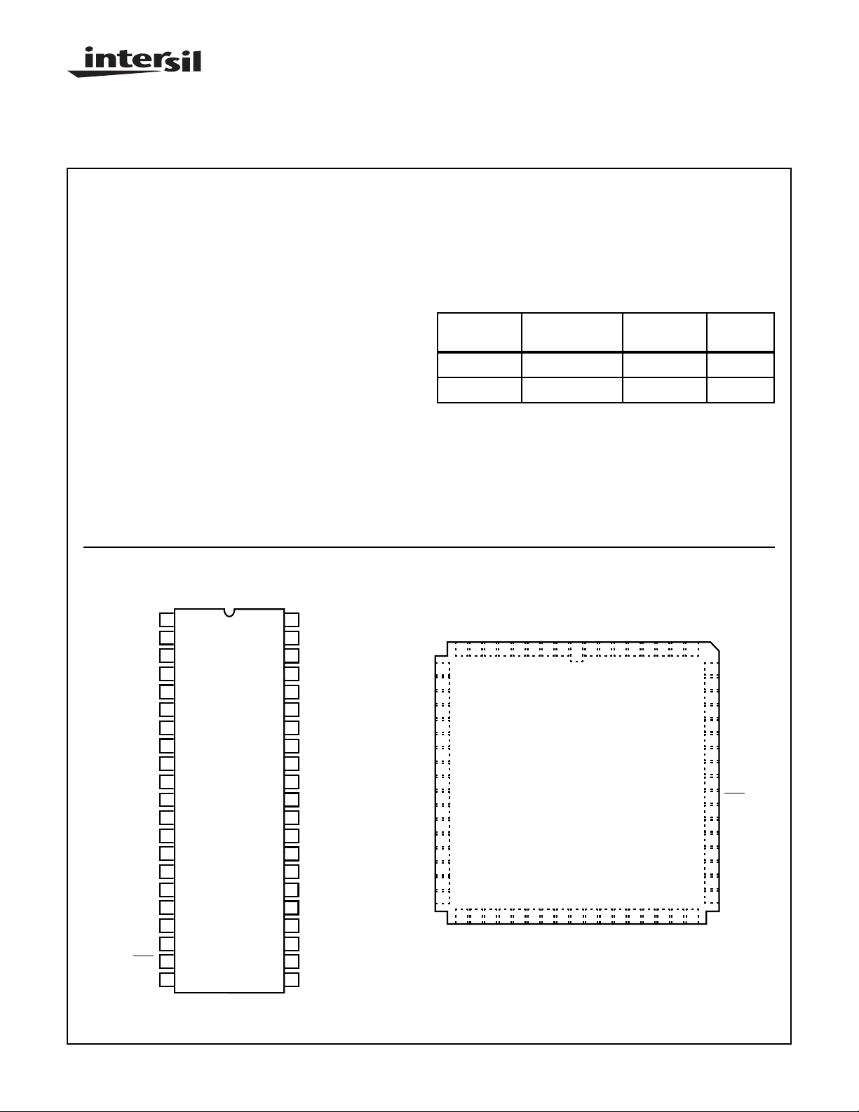
Ordering Information
PART
NUMBER
HI1396JCJ -20to 75 42 Ld SBDIP D42.6
HI1396AIL -20 to 100 68 Ld CLCC J68.A
TEMP. RANGE
(oC) PACKAGE PKG. NO.
Pinouts
AV
LINV
DV
DGND1
DGND2
(LSB) D0
(MSB) D7
DGND2
DGND2
DV
MINV
CLK
EE
NC
EE
D1
D2
D3
D4
D5
D6
EE
NC
1
2
3
4
5
6
7
8
9
10
11
12
13
14
15
16
17
18
19
20
21 2223NCCLK
HI1396 (SBDIP)
TOP VIEW
42
41
40
39
38
37
36
35
34
33
32
31
30
29
28
27
26
25
24
NC
V
RT
NC
AV
EE
AV
EE
NC
NC
AGND
V
IN
AGND
V
RM
AGND
V
IN
AGND
NC
NC
AV
EE
AV
EE
NC
V
RB
NC
AV
EE
AV
EE
NC
V
RT
NC
AV
EE
NC
NC
NC
LINV
NC
DV
EE
NC
DGND1
DGND2
NC
HI1396 (CLCC)
TOP VIEW
NCNCNCNCAGND
NC
876543216867666564636261
9
10
11
12
13
14
15
16
17
18
19
20
21
22
23
24
25
26
27
28 29 30 31 32 33 34 35 36 37 38 39 40 41 42 43
NCNCNC
NC
VINAGND
D1D2D3D4D5
(LSB) D0
VRMAGND
VINAGNDNCNCNCNC
D6
(MSB) D7
NC
DGND2
DGND1
NC
NC
NC
60
NC
59
AV
EE
58
AV
EE
57
NC
56
V
RB
55
NC
54
NC
53
NC
52
CLK
51
CLK
50
NC
49
MINV
48
NC
47
DV
EE
46
NC
45
NC
44
NC
CAUTION: These devices are sensitive to electrostatic discharge; follow proper IC Handling Procedures.
http://www.intersil.com or 407-727-9207
| Copyright © Intersil Corporation 1999
4-1156
File Number 3576.3
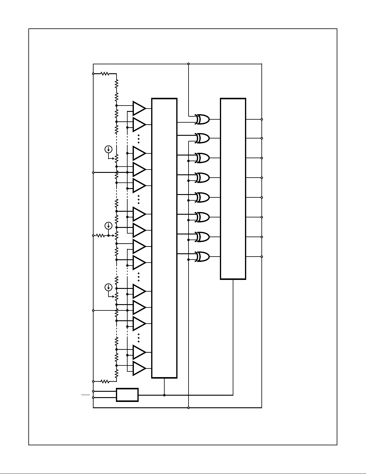
Functional Block Diagram
V
R1
RT
R/2
R
R
R
HI1396
MINV
COMPARATOR
1
D7 (MSB)
2
D6
63
R
V
IN
R2
V
RM
V
IN
64
R
65
R
126
R
127
R
128
R
129
R
191
R
192
R
193
ENCODE
LOGIC
OUTPUT
D5
D4
D3
D2
D1
D0 (LSB)
V
RB
CLK
CLK
R3
R
254
R
255
R/2
CLOCK
DRIVER
LINV
4-1157
HI1396
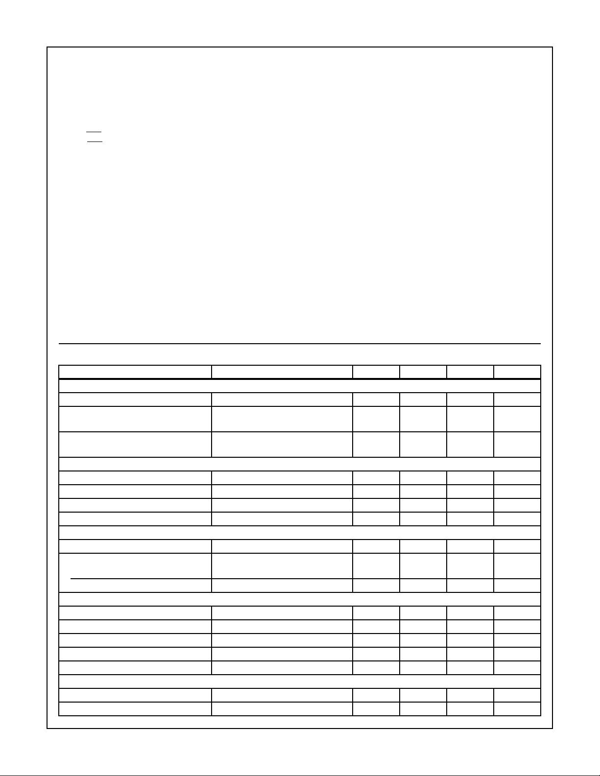
Absolute Maximum Ratings T
Supply Voltage (AVEE, DVEE) . . . . . . . . . . . . . . . . . . . . . . . . . . .-7V
Analog Input Voltage (VIN) . . . . . . . . . . . . . . . . . . . . .-2.7V to +0.5V
Reference Input Voltage
VRT, VRB, VRM . . . . . . . . . . . . . . . . . . . . . . . . . . . -2.7V to +0.5V
|VRT - VRB| . . . . . . . . . . . . . . . . . . . . . . . . . . . . . . . . . . . . . .2.5V
Digital Input Voltage
CLK, CLK, MINV, LINV . . . . . . . . . . . . . . . . . . . . . . . -4V to +0.5V
= 25oC Thermal Information
A
Thermal Resistance (Typical, Note 1) θ
SBDIP Package. . . . . . . . . . . . . . . . . . 45 7
CLCC Package . . . . . . . . . . . . . . . . . . 45 8
Maximum Junction Temperature
Ceramic Packages. . . . . . . . . . . . . . . . . . . . . . . . . . . . . . . 175oC
Maximum Storage Temperature Range (T
Maximum Lead Temperature (Soldering 10s). . . . . . . . . . . . 300oC
o
C/W θ
JA
) . . . .-65oC to 150oC
STG
JC
o
C/W
|CLK-CLK | . . . . . . . . . . . . . . . . . . . . . . . . . . . . . . . . . . . . . . .2.7V
VRM Pin Input Current (I
) . . . . . . . . . . . . . . . . . . -3mA to +3mA
VRM
Digital Output Current (ID0 to ID7). . . . . . . . . . . . . . . -30mA to 0mA
Operating Conditions (Note 1)
Temperature Ranges (Note 4)
SBDIP Package, TA . . . . . . . . . . . . . . . . . . . . . . . . -20oC to 75oC
CLCC Package, TC. . . . . . . . . . . . . . . . . . . . . . . . -20oC to 100oC
Supply Voltage Ranges
AVEE, DVEE . . . . . . . . . . . . . . . . . . . . . . . . . . . . . -5.5V to -4.95V
AVEE - DVEE. . . . . . . . . . . . . . . . . . . . . . . . . . . . . -0.05V to 0.05V
AGND - DGND . . . . . . . . . . . . . . . . . . . . . . . . . . . -0.05V to 0.05V
Reference Input Voltage
VRT. . . . . . . . . . . . . . . . . . . . . . . . . . . . . . . . . . . . . . -0.1V to 0.1V
VRB. . . . . . . . . . . . . . . . . . . . . . . . . . . . . . . . . . . . . -2.2V to -1.8V
CAUTION: Stresses above those listed in “Absolute Maxim um Ratings” ma y cause permanent damage to the device . This is a stress only rating and oper ation of
the device at these or any other conditions above those indicated in the operational sections of this specification is not implied.
NOTE:
1. θJA is measured with the component mounted on an evaluation PC board in free air.
Analog Input Voltage, VIN . . . . . . . . . . . . . . . . . . . . . . . .VRB to V
Pulse Width of Clock
t
. . . . . . . . . . . . . . . . . . . . . . . . . . . . . . . . . . . . . . . 4.0ns (Min)
PW1
t
. . . . . . . . . . . . . . . . . . . . . . . . . . . . . . . . . . . . . . . 4.0ns (Min)
PW0
RT
Electrical Specifications T
= 25oC, AVEE = DVEE = -5.2V, VRT = 0V, VRB = -2V (Note 1)
A
PARAMETER TEST CONDITIONS MIN TYP MAX UNIT
SYSTEM PERFORMANCE
Resolution - 8 - Bits
Integral Linearity Error, INL
HI1396JCJ, HI1396AIL fC = 125 MSPS - ±0.3 ±0.5 LSB
Differential Linearity Error, DNL
HI1396JCJ, HI1396AIL fC = 125 MSPS - - ±0.5 LSB
ANALOG INPUT
Input Bandwidth VIN = 2V
Analog Input Capacitance, C
Analog Input Resistance, R
Input Bias Current, I
IN
IN
IN
VIN = 1V + 0.07V
VIN = -1V 20 130 400 µA
P-P
RMS
200 - - MHz
-17-pF
50 190 - kΩ
REFERENCE INPUTS
Reference Resistance, R
REF
75 110 155 Ω
Offset Voltage
E
OT
E
OB
V
RT
V
RB
81932mV
01524mV
DIGITAL INPUTS
Logic H Level, V
Logic L Level, V
Logic H Current, I
Logic L Current, I
IH
IL
IH
IL
Input Connected to -0.8V 0 - 50 µA
Input Connected to -1.6V 0 - 50 µA
-1.13 - - V
- - -1.50 V
Input Capacitance - 7 - pF
DIGITAL OUTPUTS
Logic H Level, V
Logic L Level, V
OH
OL
RL = 50Ω to -2V -1.10 - - V
RL = 50Ω to -2V - - -1.62 V
4-1158
 Loading...