Intersil Corporation HFA5251 Datasheet

HFA5251
Data Sheet September 1998 File Number 3689.4
800MHz Monolithic Pin Driver
The HFA5251 is a very high speed monolithic pin driver
solution for high performance test systems. The device will
switch at high data rates between two input voltage levels
providing variable amplitude pulses. The output impedance
is trimmed to achieve a precision 50Ω source forimpedance
matching. TwodifferentialECL/TTLcompatibleinputs control
the operation of the HFA5251, one controlling the
V
HIGH/VLOW
switchingand the other controlling the output’s
high-impedance state. The HFA5251’s 800MHz data rate
makes it compatible with today’s high-speed VLSI test
systems and the +7V to -2V output swing allows testing of all
common logic families.
The HFA5251 is manufactured in Intersil’s proprietary
complementary bipolar UHF-1 process. The HFA5251 is
offered in die form. Contact your local sales representative
for packaging options.
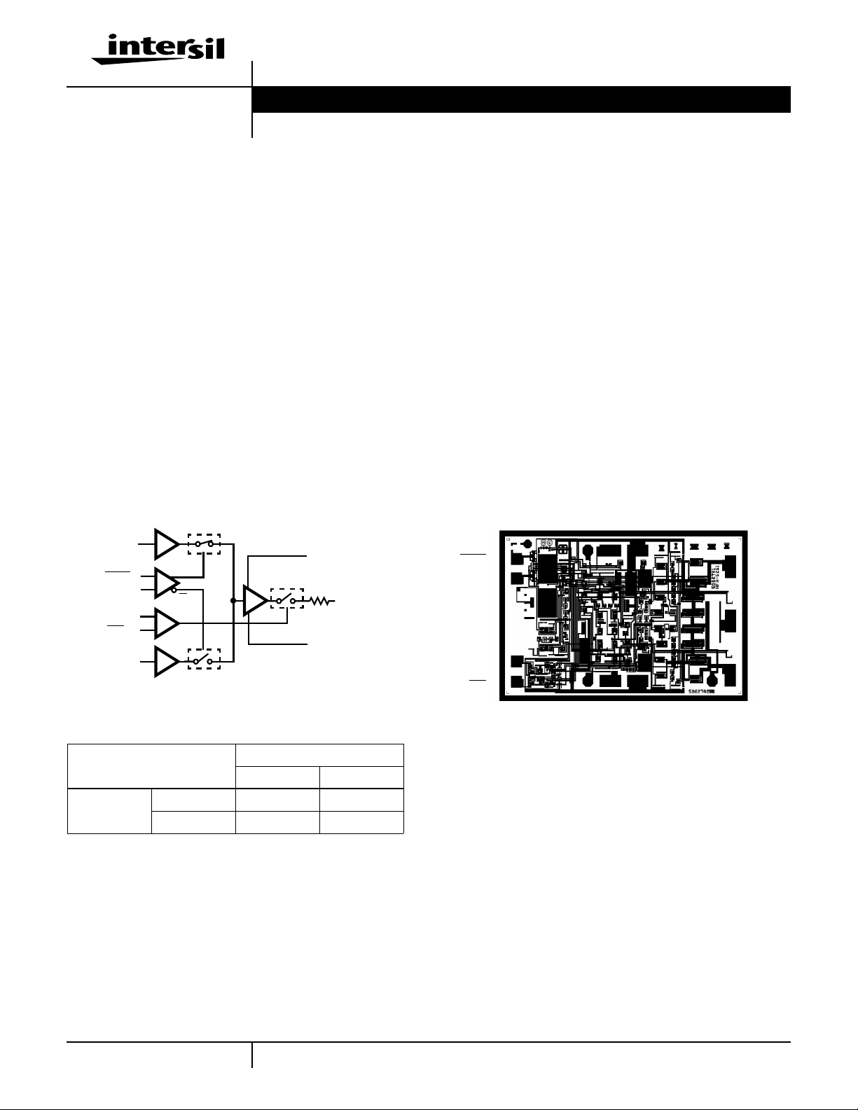
Functional Diagram
INPUT
BUFFER
V
HIGH
DATA
DAT A
HiZ
HiZ
V
LOW
HiZ 0 V
Q
-
+
Q
+
-
INPUT
BUFFER
TRUTH TABLE FOR V
1 HiZ HiZ
LOW
V
CC2
50Ω
V
OUT
V
EE2
OUT
DATA
01
V
HIGH
Features
• High Digital Data Rate . . . . . . . . . . . . . . . . . . . . . 800MHz
• Very Fast Rise/Fall Times. . . . . . . . . . . . . . . . . . . . .500ps
• Wide Output Range . . . . . . . . . . . . . . . . . . . . . +7V to -2V
• Precise 50Ω Output Impedance
• High Impedance, Three-State Output Control
Applications
• IC Tester Pin Electronics
• Pattern Generators
• Pulse Generators
• Level Comparator/Translator
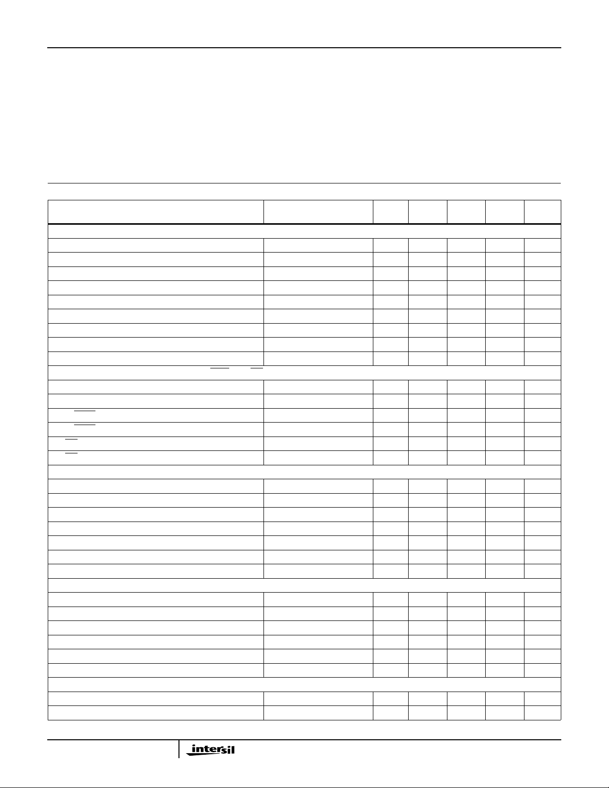
Pinout
HFA5251 (DIE FORM)
V
V
HIGH
CC1
DATA
DAT A
HiZ
HiZ
V
LOWVEE1
V
V
V
CC2
OUT
EE2
1
CAUTION: These devices are sensitive to electrostatic discharge; follow proper IC Handling Procedures.
1-888-INTERSIL or 321-724-7143
| Copyright © Intersil Corporation 1999

HFA5251
Pin Descriptions
NAME FUNCTION
V
CC1
V
EE1
V
CC2
V
EE2
V
HIGH
V
LOW
V
OUT
DATA,
DATA
HiZ,
HiZ
Positive Supply. Nominal value is 10V ±0.2V. Reducing supply voltage below 9.8V will reduce positive output voltage swing. The
totalsupply voltage from V
CC1
toV
shouldnot exceed 15.6V fornormaloperation or exceed 17.0Vto prevent damage. Intersil
EE1
recommends two wire bonds to this pad to provide the lowest possible impedance. In addition, power supply decoupling chip
capacitors of 470pF, 0.1µF and a 10µF tantalum are recommended.
Negative Supply. Nominal value is -5.2V ±0.2V. A supply voltage more positive than -5.0V will reduce negative output voltage
swing. The total supply voltage from V
CC1
to V
should not exceed 15.6V for normal operation or exceed 17.0V to prevent
EE1
damage. Intersil recommends two wire bonds to this pad to provide the lowest possible impedance. In addition, power supply
decoupling chip capacitors of 470pF, 0.1µF and a 10µF tantalum are recommended.
Output Stage Positive Supply. Nominal voltage and cautions are the same as for V
to V
and V
CC2
and V
CC2
is essential since large AC current will flow through this pad to the output during transients. Normally V
EE2
are connected together close to the die and share decoupling capacitors. Intersil recommends two wire bonds for this
pad.
Output Stage NegativeSupply. Nominal voltage and cautions are the sameas for V
to V
and V
CC2
and V
EE2
is essential since large AC current will flow through this pad to the output during transients. Normally V
EE2
are connected together close to the die and share decoupling capacitors. Intersil recommends two wire bonds for this
pad.
Input Voltage High is used to set the output high level VOH.V
high frequency noise can be achieved with a low pass filter consisting of a 50Ω chip resistor and a 470pF chip capacitor. Without
this precaution the pin driver may oscillate due to feedback from the output through the PC board ground.
Input Voltage Low is used to set the output low level VOL. V
high frequency noise can be achieved with a low pass filter consisting of a 50Ω chip resistor and a 470pF chip capacitor. Without
this precaution the pin driver may oscillate due to feedback from the output through the PC board ground.
Driver Output. The output impedance has been laser trimmed to match a 50Ω transmission line ±2Ω. Custom output impedance
trimming is available (contact sales office for details) to provide the best match possible to your 50Ω system.
Differential Digital Inputs used to switch V
OUT
to the V
HIGH
plementary ECL signals to provide optimal switching speeds and timing accuracy. However a large Common Mode and Differential Voltage Range is provided to accommodate a variety of signals including single ended TTL and CMOS. When using single
ended signals the other input must be tied to an appropriate threshold.
Differential Digital Inputs used to switch V
from an Active to a High Impedance State. Intersil recommends that this input pair
OUT
be driven by complementary ECL signals to provide optimal switching speeds and timing accuracy. However a large Common
Mode and Differential Voltage Range is provided to accommodate a variety of signals including single ended TTL and CMOS.
When using single ended signals the other input must be tied to an appropriate threshold.
. Having decoupling chip capacitors close
CC1
. Having decouplingchip capacitors close
EE1
is sensitive to capacitively coupled AC noise. Protection from
HIGH
is sensitive to capacitively coupled AC noise. Protection from
LOW
or V
level. Intersil recommends this input pair be driven by com-
LOW
CC1
EE1
2

HFA5251
Absolute Maximum Ratings Thermal Information
Supply Voltage. . . . . . . . . . . . . . . . . . . . . . . . . . . . . . . . . . . . . . 17V
Differential Input Voltage (DATA and HiZ) . . . . . . . . . . . . . . . . . . 5V
Output Current Continuous (Note 1) . . . . . . . . . . . . . . . . . . . 160mA
Input Voltage (Any pin except as specified). . . . . . . . . . VCC to V
V
Voltage. . . . . . . . . . . . . . . . . . . . . . . . . . . . . . . . . 8V to -5.5V
OUT
V
Voltage . . . . . . . . . . . . . . . . . . . . . . . . . . . . . . . . .VCC to -3V
HIGH
V
Voltage . . . . . . . . . . . . . . . . . . . . . . . . . . . . . . . . . 8V to V
LOW
V
to V
HIGH
CAUTION: Stresses above those listed in “Absolute Maximum Ratings” may cause permanent damage to the device. This is a stress only rating and operation of the
device at these or any other conditions above those indicated in the operational sections of this specification is not implied.
Voltage. . . . . . . . . . . . . . . . . . . . . . .V
LOW
HIGH
> V
EE
EE
LOW
Maximum Junction Temperature (Die) . . . . . . . . . . . . . . . . . . . 175oC
Maximum Storage Temperature Range. . . . . . . . . . -65oC to 150oC
Electrical Specifications V
= +10V, VEE = -5.2V, VIH = -0.9V, VIL = -1.75V, Unless Otherwise Specified
CC
TEMP.
PARAMETER TEST CONDITIONS
, V
INPUT CHARACTERISTICS (V
Input Offset Voltage V
V
HIGH
Input Offset Voltage V
V
LOW
Input Bias Current V
V
HIGH
Input Bias Current V
V
LOW
Voltage Range 25 -2.25 - 7.5 V
V
HIGH
V
Voltage Range 25 -2.5 - 7.25 V
LOW
to V
V
HIGH
V
HIGH/VLOW
V
HIGH/VLOW
Differential Voltage Range 25 0.25 - 10 V
LOW
Interaction at 500mV (Note 11) 25 - 2 4 mV
Interaction at 250mV (Note 11) 25 - 20 40 mV
HIGH
LOGIC INPUT CHARACTERISTICS (DATA,
)
LOW
DATA, HiZ, HiZ)
= 0V 25 -150 -50 +50 mV
OUT
= 0V 25 -150 -50 +50 mV
OUT
= -2.25V to +7.5V 25 -50 110 300 µA
HIGH
= -2.5V to +7.25V 25 -300 -110 50 µA
LOW
(oC) MIN TYP MAX UNITS
Logic Input Voltage Range 25 -2 - 7 V
Logic Differential Input Voltage 25 0.4 - 5 V
DATA Logic Input High Current VIH = 0V, VIL = -2V 25 -50 110 300 µA
DATA/
DATA Logic Input Low Current VIH = 0V, VIL = -2V 25 -700 -300 50 µA
DATA/
HiZ Logic Input High Current VIH = 0V, VIL = -2V 25 -50 70 200 µA
HiZ/
HiZ Logic Input Low Current VIH = 0V, VIL = -2V 25 -300 -80 50 µA
HiZ/
TRANSFER CHARACTERISTICS
Voltage Gain V
V
HIGH
Voltage Gain V
V
LOW
V
HIGH/VLOW
V
HIGH/VLOW
V
HIGH/VLOW
V
HIGH
V
HIGH/VLOW
SWITCHING CHARACTERISTICS (Z
Linearity Error (Note 7) Fullscale = 5V 25 -0.5 - 0.5 %
Linearity Error (Note 8) Fullscale = 8.5V 25 -0.75 - 0.75 %
End Point Gain Deviation (Notes 10, 13) 0.5V Steps 25 -2.0 - 2.0 %
End Point Gain Error (Notes 10 and 14) V
-3dB Bandwidth 200mV
= 16 inches of RG-58 Terminated with 50Ω)
LOAD
= -1V to 6.5V 25 0.95 - 1 V/V
HIGH
= -1.5V to 6V 25 0.95 - 1 V/V
LOW
= 6.7V to 7.0V 25 -20 - 20 mV
OUT
P-P
25 - 100 - MHz
Propagation Delay (Notes 2, 17) 25 0.8 - 1.5 ns
Propagation Delay Match (Notes 2, 17) Rising to Falling Edge 25 -100 - 100 ps
Rising Edge Propagation Delay vs Duty Cycle (Notes 12, 17) 25 -120 -20 80 ps
Falling Edge Propagation Delay vs Duty Cycle (Notes 12, 17) 25 -80 20 120 ps
Active to HiZ Delay (Note 17) 25 1.2 1.7 2.2 ns
HiZ to Active Delay (Note 17) 25 2.1 2.6 3.1 ns
TRANSIENT RESPONSE (Z
Rise/Fall Time (20%-80%) 1V
Rise/Fall Time (10%-90%) 3V
= 16 inches of RG-58 Terminated with 5pF)
LOAD
P-P
P-P
25 - 450 500 ps
25 - 890 1000 ps
3
 Loading...