Intersil Corporation HFA3861BIN96, HFA3861BIN Datasheet
TM
Data Sheet February 2002
Direct Sequence Spread Spectrum
Baseband Processor
The Intersil HFA3861B Direct
Sequence Spread Spectrum (DSSS)
baseband processor is part of the
PRISM® 2.4GHz WLAN Chip Set,
and contains all the functions necessary for a full or half
duplex packet baseband transceiver.
The HFA3861B has on-board A/D’s and D/A for analog I and
Q inputs and outputs, for which the HFA3783 IF QMODEM is
recommended. Differential phase shift keying modulation
schemes DBPSK and DQPSK, with data scrambling
capability, are available along with Complementary Code
Keying to provide a variety of data rates. Built-in flexibility
allows the HFA3861B to be configured through a general
purpose control bus, for a range of applications. Both
Receive and Transmit AGC functions with 7-bit AGC control
obtain maximum performance in the analog portions of the
transceiver. The HFA3861B is housed in a thin plastic quad
flat package (TQFP) suitable for PCMCIA board
applications.
Ordering Information
TEMP.
PART NUMBER
RANGE (oC) PACKAGE PKG. NO.
HFA3861BIN -40 to 85 64 Ld TQFP Q64.10x10
HFA3861BIN96 -40 to 85 Tape and Reel
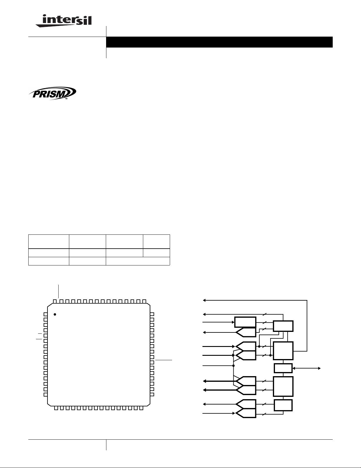
Pinout
HFA3861B
FN4816.2
Features
• Complete DSSS Baseband Processor
• Processing Gain. . . . . . . . . . . . . . . . . . . . FCC Compliant
• Programmable Data Rate. . . . . . . . 1, 2, 5.5, and 11Mbps
• Ultra Small Package. . . . . . . . . . . . . . . . . . . . . 10 x 10mm
• Single Supply Operation (44MHz Max) . . . . . 2.7V to 3.6V
• Modulation Methods. . . . . . . . DBPSK, DQPSK, and CCK
• Supports Full or Half Duplex Operations
• On-Chip A/D and D/A Converters for I/Q Data (6-Bit,
22MSPS), AGC, and Adaptive Power Control (7-Bit)
•Targeted for Multipath Delay Spreads ~50ns
• Supports Short Preamble Acquisition
• Supports Antenna Diversity
Applications
• Enterprise WLAN Systems
• Systems Targeting IEEE 802.11 Standard
• DSSS PCMCIA Wireless Transceiver
• Spread Spectrum WLAN RF Modems
• TDMA Packet Protocol Radios
•Part 15 Compliant Radio Links
•Portable PDA/Notebook Computer
• Wireless Digital Audio, Video, Multimedia
• PCN/Wireless PBX
• Wireless Bridges
GNDd
V
DDD
SD
SCLK
R/W
CS
GNDd
V
DDD
GNDa
RX_I+
RX_IV
DDA
RX_Q+
RX_Q-
GNDa
V
REF
ESET
SDI
R
TX_PE
RX_PE
CCA
6463 62 61 60 59 58 57 56 55 54 53 52 51 50 49
1
2
3
4
5
6
7
8
9
10
11
12
13
14
15
16
17 18 19 20 21 22 23 24 25 26 27 28 29 30 31 32
DDA
V
RX-IF_DET
TX_AGC_IN
I
GNDa
REF
TX_RDY
V
DDA
TXD
V
TX_I-
TX_I+
DDD
GNDd
GNDa
TXCLK
MD_RDY
RXD
GNDa
TX_Q+
COMPRES2
COMPCAP2
RXCLK
TEST7
TX_Q-
1
TEST6
TEST5
TEST4
48
TEST3
47
TEST2
46
TEST1
45
TEST0
44
GNDd
43
MCLK
42
NC
41
ANT-SEL
40
A
NT-SEL
39
RX-RF_AGC
38
V
37
DDD
GNDd
36
TX_IF_AGC
35
RX_IF_AGC
34
COMPCAP1
33
DDA
V
COMPRES1
CAUTION: These devices are sensitive to electrostatic discharge; follow proper IC Handling Procedures.
PRISM® is a registered trademark of Intersil Corporation. PRISM and design is a trademark of Intersil Corporation.
Simplified Block Diagram
ANT_SEL
RX_RF_AGC
RX_IF_DET
RX_IF_AGC
RX_I±
RX_Q±
V
REF
TX_I±
TX_Q±
TX_IF_AGC
TX_AGC_IN
44MHz MCLK
1-888-INTERSIL or 321-724-7143
THRESH.
DETECT
|
Intersil (and design) is a trademark of Intersil Americas Inc.
Copyright © Intersil Americas Inc. 2002. All Rights Reserved
IF
DAC
I ADC
Q ADC
I DAC
Q DAC
TX
DAC
TX
ADC
1
1
AGC
7
CTL
6
DEMOD
6
I/O
6
6
MOD
7
6
TX
ALC
HFA 3861B BBP
DATA I/O
Typical Application Diagram
AntSel
2
PLL
HFA3963
RFPA
(FILE# 4635)
HFA3683A RF/IF
CONV (FILE# 4634)
Σ
REF IN
RF
LO
Σ
REF IN
I/O LO
PLL
HFA3783 QUAD IF
(FILE# 4633)
REFOUT
IF
LO
RF
DAC
RF
ADC
IF
DAC
I ADC
Q ADC
I DAC
Q DAC
TX
DAC
TX
ADC
REF IN
1
1
AGC
7
CTL
6
DEMOD
6
I/O
6
6
MOD
7
TX
ALC
6
HFA3861B BBP
(FILE# 4816)
RADIO
DATA
INTERFACE
RADIO
CONTROL
PORTS
GP SERIAL
PORTS
WEP
ENGINE
CPU
16-BIT
PIPELINED
CONTROL
PROCESSOR
HFA3841
(FILE# 4661)
INTERFACE
MEMORY
ACCESS
ARBITER
EXTERNAL
MEMORY
MAC
HOST
LOGIC
HOSTPC
INTERFACE
HFA3861B
T/Rsw
DIFFERENTIAL SIGNALS
44MHz MCLK
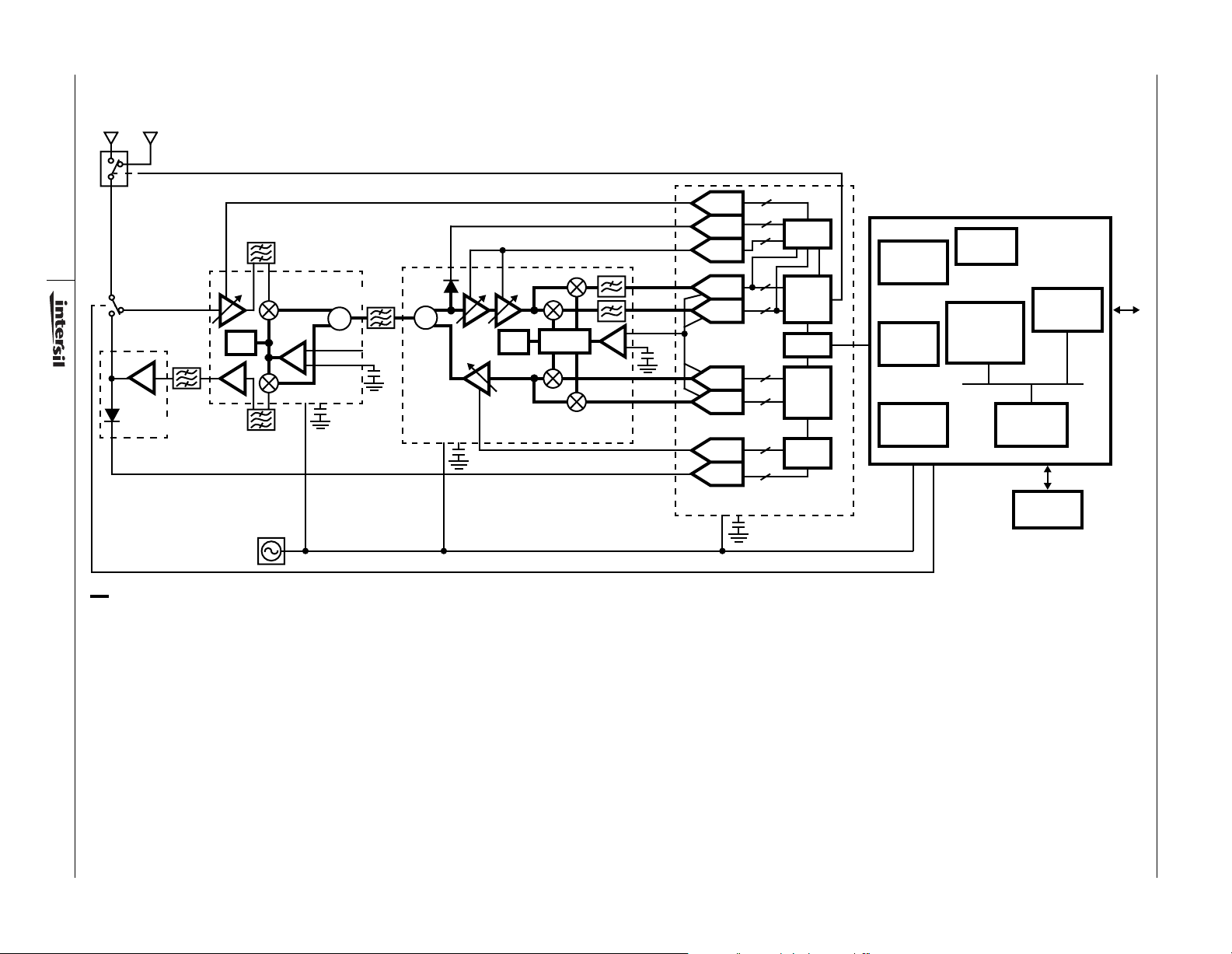
TYPICAL TRANSCEIVER APPLICATION CIRCUIT USING THE HFA3861B
For additional information on the PRISM® chip set, visit our web site
www.intersil.com or call 1-888-INTERSIL or 321-724-7143.

HFA3861B
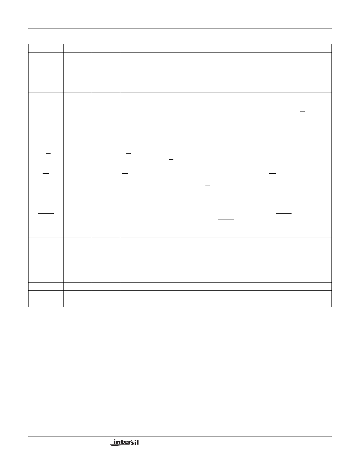
Pin Descriptions
NAME PIN TYPE I/O DESCRIPTION
V
(Analog) 12, 17, 22, 31Power DC power supply 2.7V - 3.6V (Not Hard wired Together On Chip).
DDA
V
(Digital) 2, 8, 37, 57 Power DC power supply 2.7 - 3.6V.
DDD
GNDa
(Analog)
GNDd (Digital) 1, 7, 36, 43, 56Ground DC power supply 2.7 - 3.6V, ground.
9, 15, 20,
25, 28,
Ground DC power supply 2.7 - 3.6V, ground (Not Hard wired Together On Chip).
V
REF
I
REF
RXI
, +/-
RXQ
, +/-
ANTSEL
ANTSEL 40 O The antenna select signal changes state as the receiver switches from antenna to antenna during the
RX_IF_DET 19 I Analog input to the receive power A/D converter for AGC control.
RX_IF_AGC 34 O Analog drive to the IF AGC control.
RX_RF_AGC 38 O Drive to the RF AGC stage attenuator. CMOS digital.
TX_AGC_IN 18 I Input to the transmit power A/D converter for transmit AGC control.
TX_IF_AGC 35 O Analog drive to the transmit IF power control.
TX_PE 62 I When active, the transmitter is configured to be operational, otherwise the transmitter is in standby
TXD 58 I TXD is an input, used to transfer MAC Payload Data Unit (MPDU) data from the MAC or network
TXCLK 55 O TXCLK is a clock output used to receive the data on the TXD from the MAC or network processor to
TX_RDY 59 O TX_RDY is an output to the external network processor indicating that Preamble and Header
CCA 60 O Clear Channel Assessment (CCA) is an output used to signal that the channel is clear to transmit. The
RXD 53 O RXD is an output to the external network processor transferring demodulated Header information and
RXCLK 52 O RXCLK is the bit clock output. This clock is used to transfer Header information and payload data
16 I Voltage reference for A/D’s and D/A’s.
21 I Current reference for internal ADC and DAC devices. Requires a 12k
10/11 I Analog input to the internal 6-bit A/D of the In-phase received data. Balanced differential 10+/11-.
13/14 I Analog input to the internal 6-bit A/D of the Quadrature received data. Balanced differential 13+/14-.
39 O The antenna select signal changes state as the receiver switches from antenna to antenna during the
acquisition process in the antenna diversity mode. This is a complement for ANTSEL (pin 40) for
differential drive of antenna switches.
acquisition process in the antenna diversity mode. This is a complement for ANTSEL (pin 39) for
differential drive of antenna switches.
mode. TX_PE is an input from the external Media Access Controller (MAC) or network processor to
the HFA3861B. The rising edge of TX_PE will start the internal transmit state machine and the falling
edge will initiate shut down of the state machine. TX_PE envelopes the transmit data except for the
last bit. The transmitter will continue to run for 4
down gracefully.
processor to the HFA3861B. The data is received serially with the LSB first. The data is clocked in the
HFA3861B at the rising edge of TXCLK.
the HFA3861B, synchronously. Transmit data on the TXD bus is clocked into the HFA3861B on the
rising edge. The clocking edge is also programmable to be on either phase of the clock. The rate of
the clock will be dependent upon the data rate that is programmed in the signalling field of the header.
information has been generated and that the HFA3861B is ready to receive the data packet from the
network processor over the TXD serial bus.
CCA may be configured to one of four possible algorithms. The CCA algorithm and its features are
described elsewhere in the data sheet.
Logic 0 = Channel is clear to transmit.
Logic 1 = Channel is NOT clear to transmit (busy).
This polarity is programmable and can be inverted.
data in a serial format. The data is sent serially with the LSB first. The data is frame aligned with
MD_RDY.
through the RXD serial bus to the network processor. This clock reflects the bit rate in use. RXCLK is
held to a logic “0” state during the CRC16 reception. RXCLK becomes active after the SFD has been
detected. Data should be sampled on the rising edge. This polarity is programmable and can be
inverted.
µ s after TX_PE goes inactive to allow the PA to shut
Ω resistor to ground.
3
HFA3861B
Pin Descriptions
NAME PIN TYPE I/O DESCRIPTION
MD_RDY 54 O MD_RDY is an output signal to the network processor, indicating header data and a data packet are
RX_PE 61 I When active, the receiver is configured to be operational, otherwise the receiver is in standby mode.
SD 3 I/O SD is a serial bidirectional data bus which is used to transfer address and data to/from the internal
SCLK 4 I SCLK is the clock for the SD serial bus. The data on SD is clocked at the rising edge. SCLK is an input
SDI 64 I Serial Data Input in 3 wire mode described in Tech Brief 383. This pin is not used in the 4 wire interface
R/W 5IR/W is an input to the HFA3861B used to change the direction of the SD bus when reading or writing
CS 6ICS is a Chip select for the device to activate the serial control port. The CS doesn’t impact any of the
TEST 7:0 51, 50, 49,
48, 47, 46,
RESET 63 I Master reset for device. When active TX and RX functions are disabled. If RESET is kept low the
MCLK 42 I Master Clock for device. The nominal frequency of this clock is 44MHz. This is used internally to
TXI
+/-
TXQ
+/-
CompCap 33 I Compensation Capacitor.
CompCap2 26 I Compensation Capacitor.
CompRes1 32 I Compensation Resistor.
CompRes2 27 I Compensation Resistor.
NOTE: See CR10[3].
(Continued)
ready to be transferred to the processor. MD_RDY is an active high signal that signals the start of data
transfer over the RXD serial bus. MD_RDY goes active when the SFD (Note) is detected and returns
to its inactive state when RX_PE goes inactive or an error is detected in the header.
This is an active high input signal. In standby, RX_PE inactive, all RX A/D converters are disabled.
registers. The bit ordering of an 8-bit word is MSB first. The first 8 bits during transfers indicate the
register address immediately followed by 8 more bits representing the data that needs to be written or
read at that register. In the 4 wire interface mode, this pin is three-stated unless the R/W
clock and it is asynchronous to the internal master clock (MCLK). The maximum rate of this clock is
11MHz or one half the master clock frequency, whichever is lower.
described in this data sheet. It should not be left floating.
data on the SD bus. R/W must be set up prior to the rising edge of SCLK. A high level indicates read
while a low level is a write.
other interface ports and signals, i.e., the TX or RX ports and interface signals. This is an active low
signal. When inactive SD, SCLK, and R/W become “don’t care” signals.
I/O This is a data port that can be programmed to bring out internal signals or data for monitoring. These
bits are primarily reserved by the manufacturer for testing. A further description of the test port is given
45, 44
23/24 O TX Spread baseband I digital output data. Data is output at the chip rate. Balanced differential 23+/24-.
29/30 O TX Spread baseband Q digital output data. Data is output at the chip rate. Balanced differential
in the appropriate section of this data sheet.
HFA3861B goes into the power standby mode. RESET does not alter any of the configuration register
values nor does it preset any of the registers into default values. Device requires programming upon
power-up See the section on Control Register 12 bit 7 for important initialization information.
generate all other internal necessary clocks and is divided by 2 or 4 for the transceiver clocks.
29+/30-.
pin is high.
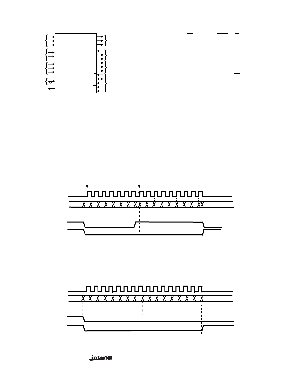
External Interfaces
There are three primary digital interface ports for the
HFA3861B that are used for configuration and during
normal operation of the device as shown in Figure 1. These
ports are:
• The
Control Port
read the status of the internal HFA3861B registers.
• The
TX Port
to be transmitted from the network processor.
• The
RX Port
demodulated data to the network processor.
In addition to these primary digital interfaces the device
includes a byte wide parallel
, which is used to configure, write and/or
, which is used to accept the data that needs
, which is used to output the received
Test Port
which can be
4
configured to output various internal signals and/or data. The
device can also be set into various power consumption
modes by external control. The HFA3861B contains three
Analog to Digital (A/D) converters and four Digital to Analog
converters. The analog interfaces to the HFA3861B include,
the In phase (I) and quadrature (Q) data component inputs/
outputs, and the RF and IF receive automatic gain control
and transmit output power control.
HFA3861B
HFA3861B
ANALOG
INPUTS
REFERENCE
A/D
POWER
DOWN
SIGNALS
TEST
PORT
ANT_SEL
8
RXI
RXQ
AGC
V
REF
I
REF
TX_PE
RX_PE
RESET
TEST
AGC
TXI
TXQ
TXD
TXCLK
TX_RDY
RXD
RXC
MD_RDY
CS
SD
SCLK
R/W
SDI
ANALOG
OUTPUTS
TX_PORT
RX_PORT
CONTROL_PORT
FIGURE 1. EXTERNAL INTERFACES
Control Port (4 Wire)
The serial control port is used to serially write and read
data to/from the device. This serial port can operate up to a
11MHz rate or 1/2 the maximum master clock rate of the
device, MCLK (whichever is lower). MCLK must be running
and RESET must be inactive during programming. This
port is used to program and to read all internal registers.
The first 8 bits always represent the address followed
immediately by the 8 data bits for that register. The LSB of
the address is a don’t care, but reserved for future
expansion. The serial transfers are accomplished through
the serial data pin (SD). SD is a bidirectional serial data
bus. Chip Select (CS
), and Read/Write (R/W) are also
required as handshake signals for this port. The clock used
in conjunction with the address and data on SD is SCLK.
This clock is provided by the external source and it is an
input to the HFA3861B. The timing relationships of these
signals are illustrated in Figures 2 and 3. R/W
data is to be read, and low when it is to be written. CS
asynchronous reset to the state machine. CS
active (low) during the entire data transfer cycle. CS
is high when
is an
must be
selects
the serial control port device only. The serial control port
operates asynchronously from the TX and RX ports and it
can accomplish data transfers independent of the activity at
the other digital or analog ports.
The HFA3861B has 96 internal registers that can be
configured through the control port. These registers are
listed in the Configuration and Control Internal Register
table. Table 9 lists the configuration register number, a brief
name describing the register, the HEX address to access
each of the registers and typical values. The type indicates
whether the corresponding register is Read only (R) or
Read/Write (R/W). Some registers are two bytes wide as
indicated on the table (high and low bytes).
FIRST ADDRESS BIT FIRST DATABIT OUT
SCLK
SD
R/W
CS
7654321076543210
1234567 01234567
LSB DATA OUTMSBMSB ADDRESS IN
NOTES:
1. The HFA3861B always uses the rising edge of SCLK to sample address and data and to generate read data.
2. These figures show the controller using the falling edge of SCLK to generate address and data and to sample read data.
FIGURE 2. CONTROL PORT READ TIMING
SCLK
SD
R/W
7654321076543210
1234567 012345670
LSB DATA INMSBMSB ADDRESS IN
CS
FIGURE 3. CONTROL PORT WRITE TIMING
5
HFA3861B
TX Port
The transmit data port accepts the data that needs to be
transmitted serially from an external data source. The data is
modulated and transmitted as soon as it is received from the
external data source. The serial data is input to the HFA3861B
through TXD using the next rising edge of TXCLK to clock it in
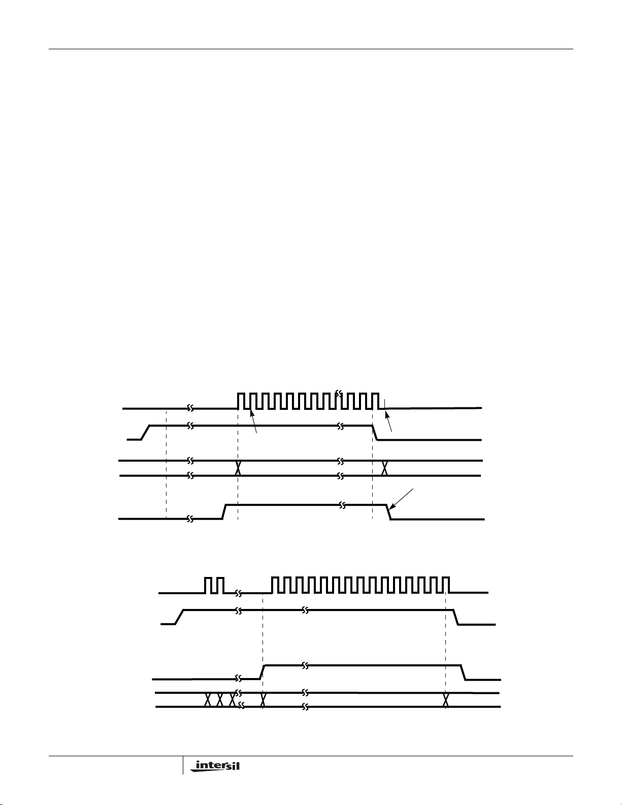
the HFA3861B. TXCLK is an output from the HFA3861B. A
timing scenario of the transmit signal handshakes and
sequence is shown on timing diagram Figure 4.
The external processor initiates the transmit sequence by
asserting TX_PE. TX_PE envelopes the transmit data packet
on TXD. The HFA3861B responds by generating a Preamble
and Header. Before the last bit of the Header is sent, the
HFA3861B begins generating TXCLK to input the serial data
on TXD. TXCLK will run until TX_PE goes back to its inactive
state indicating the end of the data packet. The user needs to
hold TX_PE high for as many clocks as there bits to transmit.
For the higher data rates, this will be in multiples of the
number of bits per symbol. The HFA3861B will continue to
output modulated signal for 4
to supply bits to flush the modulation path. TX_PE must be
held until the last data bit is output from the MAC/FIFO. The
minimum TX_PE inactive pulse required to restart the
preamble and header generation is 2.22
modulator is 4.22
µ
s.
µ
s after the last data bit is output,
µ s and to reset the
The HFA3861B internally generates the preamble and header
information from information supplied via the control registers.
The external source needs to provide only the data portion of
the packet and set the control registers. The timing diagram of
this process is illustrated on Figure 4. Assertion of TX_PE will
initialize the generation of the preamble and header. TX_RDY,
which is an output from the HFA3861B, is used (if needed) to
indicate to the external processor that the preamble has been
generated and the device is ready to receive the data packet
(MPDU) to be transmitted from the external processor.
Signals TX_RDY, TX_PE and TXCLK can be set individually,
by programming Configuration Register (CR) 1, as either
active high or active low signals.
The transmit port is completely independent from the
operation of the other interface ports including the RX port,
therefore supporting a full duplex mode.
RX Port
The timing diagram Figure 5 illustrates the relationships
between the various signals of the RX port. The receive data
port serially outputs the demodulated data from RXD. The
data is output as soon as it is demodulated by the HFA3861B.
RX_PE must be at its active state throughout the receive
operation. When RX_PE is inactive the device's receive
functions, including acquisition, will be in a stand by mode.
TXCLK
TX_PE
TXD
TX_RDY
NOTE: Preamble/Header and Data is transmitted LSB first. TXD shown generated from rising edge of TXCLK.
RXCLK
RX_PE
HEADER
FIELDS
PROCESSING
MD_RDY
RXD
PREAMBLE/HEADER
FIRST DATA BIT SAMPLED
LSB DATA PACKET
FIGURE 4. TX PORT TIMING
LSB DATA PACKET MSB
MSB
DATA
LAST DATA BIT SAMPLED
DEASSERTED WHEN LAST
CHIP OF MPDU CLEARS
MOD PATH OF 3861 EXCEPT FOR
TX FILTER AND D/A
NOTE: MD_RDY active after CRC16. See detailed timing diagrams (Figures 18, 19, 20).
FIGURE 5. RX PORT TIMING
6
7
HFA3861B
RXCLK is an output from the HFA3861B and is the clock for
the serial demodulated data on RXD. MD_RDY is an output
from the HFA3861B and it may be set to go active after the
SFD or CRC fields. Note that RXCLK becomes active after
the Start Frame Delimiter (SFD) to clock out the Signal,
Service, and Length fields, then goes inactive during the
header CRC field. RXCLK becomes active again for the
data. MD_RDY returns to its inactive state after RX_PE is
deactivated by the external controller, or if a header error is
detected. A header error is either a failure of the CRC
check, or the failure of the received signal field to match
one of the 4 programmed signal fields. For either type of
header error, the HFA3861B will reset itself after reception
of the CRC field. If MD_RDY had been set to go active after
CRC, it will remain low.
MD_RDY and RXCLK can be configured through CR 1, bits
1 and 0 to be active low, or active high. The receive port is
completely independent from the operation of the other
interface ports including the TX port, supporting therefore a
full duplex mode.
RX I/Q A/D Interface
The PRISM baseband processor chip (HFA3861B) includes
two 6-bit Analog to Digital converters (A/Ds) that sample the
balanced differential analog input from the IF down
converter. The I/Q A/D clock, samples at twice the chip rate.
The nominal sampling rate is 22MHz.
The interface specifications for the I and Q A/Ds are listed in
Ta ble 1. The HFA3861B is designed to be DC coupled to the
HFA3783.
TABLE 1. I, Q, A/D SPECIFICATIONS
PARAMETER MIN TYP MAX
Full Scale Input Voltage (V
Input Bandwidth (-0.5dB) - 11MHz -
Input Capacitance (pF) - 2 -
Input Impedance (DC) 5k
(Sampling Frequency) - 22MHz -
f
S
The voltages applied to pin 16, V
the references for the internal I and Q A/D converters. In
addition, For a nominal I/Q input of 250mV
suggested V
voltage is 1.2V.
REF
) 0.90 1.00 1.10
P-P
Ω
and pin 21, I
REF
HFA3683 HFA3783
--
, the
P-P
REF
set
RX_RF_AGC
RX_IF_DET
RX_IF_AGC
RX_I±
RX_Q±
AGC Circuit
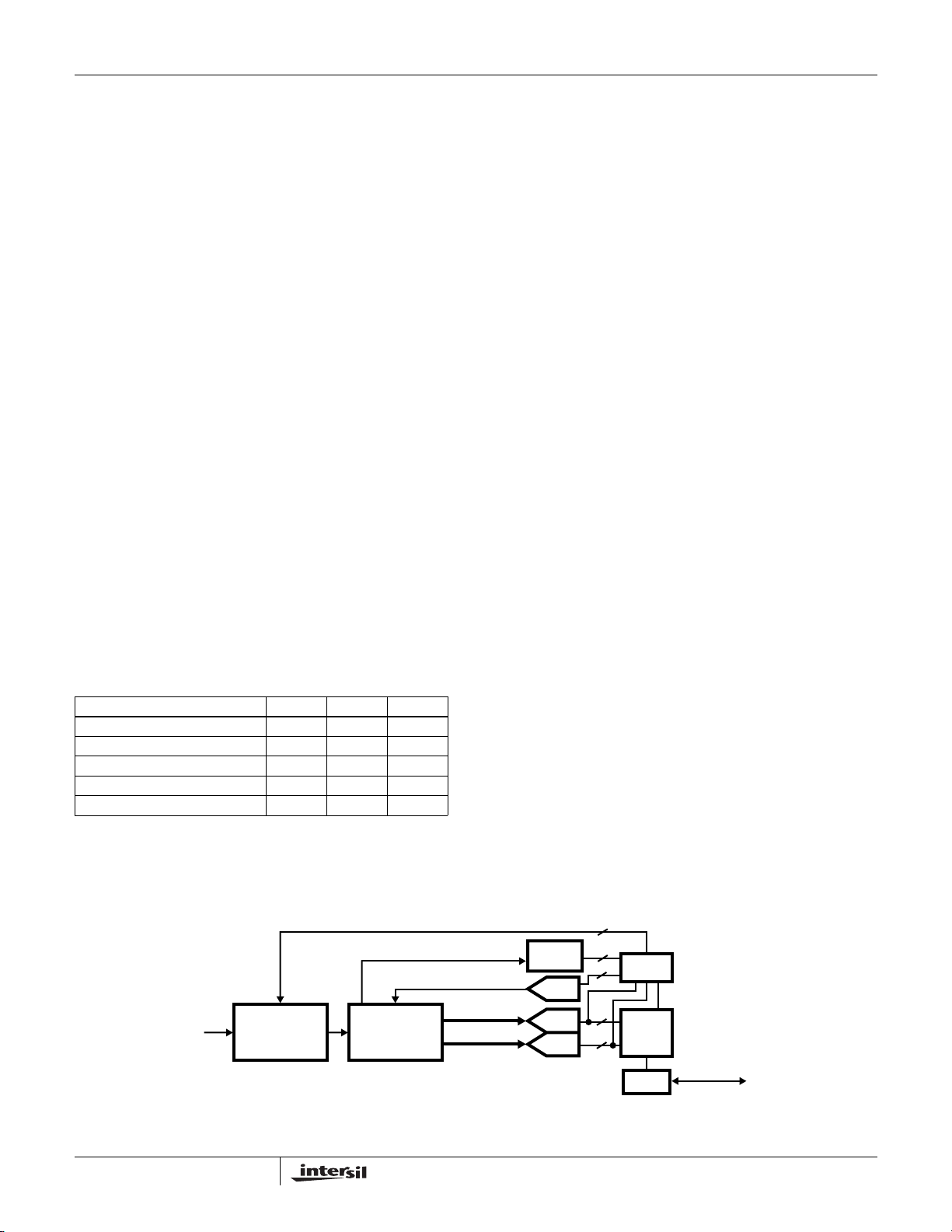
The AGC circuit is designed to optimize A/D performance for
the I and Q inputs by maintaining the proper headroom on
the 6-bit converters. There are two gain stages being
controlled. At RF, the gain control is a 30dB step in gain from
turning off the LNA. This RF gain control optimizes the
receiver dynamic range when the signal level is high and
maintains the noise figure of the receiver when it is needed
most. At IF the gain control is linear and covers the bulk of
the gain control range of the receiver.
The AGC sensing mechanism uses a combination of the
I and Q A/D converters and the detected signal level in the IF
to determine the gain settings. The A/D outputs are
monitored in the HFA3861B for the desired nominal level.
When it is reached, by adjusting the receiver gain, the gain
control is locked for the remainder of the packet.
RX_AGC_IN Interface
The signal level in the IF stage is monitored to determine
when to impose the up to 30dB gain reduction in the RF
stage. This maximizes the dynamic range of the receiver by
keeping the RF stages out of saturation at high signal levels.
When the IF circuits’ sensor output reaches 0.5V, the
HFA3861B comparator switches in the 30dB pad and
compensates the IF AGC and RSSI measures.
TX I/Q DAC Interface
The transmit section outputs balanced differential analog
signals from the transmit DACs to the HFA3783. These are
DC coupled and digitally filtered.
Test Port
The HFA3861B provides the capability to access a number of
internal signals and/or data through the Test port, pins TEST
7:0. The test port is programmable through configuration
register (CR 34). Any signal on the test port can also be read
from configuration register (CR50) via the serial control port.
Additionally, the transmit DACs can be configured to show
signals in the receiver via CR 14. This allows visibility to
analog like signals that would normally be very difficult to
capture.
1
THRESH.
DETECT
DAC
I ADC
Q ADC
1
AGC
7
6
6
CTL
DEMOD
IF
HFA3861B
FIGURE 6. AGC CIRCUIT
I/O
DATA I/O

HFA3861B
TX
RX
Power Down Modes
The power consumption modes of the HFA3861B are
controlled by the following control signals.
Receiver Power Enable (RX_PE, pin 61), which disables the
receiver when inactive.
Tr ansmitter Power Enable (TX_PE, pin 62), which disables
the transmitter when inactive.
Reset (RESET
mode. The power down mode where, both RESET
RX_PE are used is the lowest possible power consumption
mode for the receiver. Exiting this mode requires a
maximum of 10
The contents of the Configuration Registers are not effected
by any of the power down modes. No reconfiguration is
required when returning to operational modes. Activation of
RESET does corrupt learned values of AGC settings and
noise floor values. Optimum receiver operation may not be
achieved until these values are reestablished (typically
<50
µ
s of operation in noise only needed). The power
savings of activating RESET must be weighed against this.
Ta ble 2 describes the power down modes available for the
HFA3861B (V
other inputs to the part (MCLK, SCLK, etc.) continue to run
except as noted.
, pin 63), which puts the receiver in a sleep
and
µ
s before the device is operational.
= 3.3V). The table values assume that all
CC
Transmitter Description
The HFA3861B transmitter is designed as a Direct
Sequence Spread Spectrum Phase Shift Keying (DSSS
PSK) modulator. It can handle data rates of up to 11Mbps
(refer to AC and DC specifications). The various modes of
the modulator are Differential Binary Phase Shift Keying
(DBPSK) for 1Mbps, Differential Quaternary Phase Shift
Keying (DQPSK) for 2Mbps, and Complementary Code
Keying (CCK) for 5.5Mbps and 11Mbps. These implement
data rates as shown in Table 3. The major functional blocks
of the transmitter include a network processor interface,
DPSK modulator, high rate modulator, a data scrambler and
a spreader, as shown in Figure 7. CCK is essentially a
quadra-phase form of M-ARY Orthogonal Keying. A
description of that modulation can be found in Chapter 5 of:
“Telecommunications System Engineering”, by Lindsey and
Simon, Prentis Hall publishing.
The preamble is always transmitted as the DBPSK
waveform while the header can be configured to be either
DBPSK, or DQPSK, and data packets can be configured for
DBPSK, DQPSK, or CCK. The preamble is used by the
receiver to achieve initial PN synchronization while the
header includes the necessary data fields of the
communications protocol to establish the physical layer
link. The transmitter generates the synchronization
preamble and header and knows when to make the DBPSK
to DQPSK or CCK switchover, as required.
TABLE 2. POWER DOWN MODES
AT
MODE RX_PE TX_PE RESET
SLEEP
STANDBY Inactive Inactive Inactive 1.5mA Both transmit and receive operations disabled. Device will resume its operational
NO CLOCK
DATA
MODULATION
DBPSK 22 00 00 1 1
DQPSK 22 01 01 2 1
CCK 22 10 10 5.5 1.375
CCK 22 11 11 11 1.375
Inactive Inactive Active 1mA Both transmit and receive functions disabled. Device in sleep mode. Control
Inactive Active Inactive 15mA Receiver operations disabled. Receiver will return in its operational state within 1 µ s
Active Inactive Inactive 50mA Transmitter operations disabled. Transmitter will return to its operational state within
Standby Active 300
I
CC
TABLE 3. BIT RATE TABLE EXAMPLES FOR MCLK = 44MHz
A/D SAMPLE CLOCK
(MHz)
44MHz DEVICE STATE
Interface is still active. Register values are maintained. Device will return to its active
state within 10
state within 1 µ s of RX_PE or TX_PE going active.
of RX_PE going active.
2 MCLKs of TX_PE going active.
µ A All inputs at V
TX SETUP CR 5
BITS 1, 0
µ s.
or GND.
CC
RX SIGNAL CR 63
BITS 7, 6 DATA RATE (Mbps)
SYMBOL RATE
(MSPS)
8
HFA3861B
9
DATA
I
OUT
Q
OUT
CHIP
RATE
SYMBOL
RATE
I vs Q
802.11 DSSS BPSK 802.11 DSSS QPSK
1Mbps
BARKER
1 BIT ENCODED TO
ONE OF 2 CODE
WORDS
(TRUE-INVERSE)
11 CHIPS
11 MC/S 11 MC/S
1 MS/S 1 MS/S
2 BITS ENCODED
TO ONE OF
4 CODE WORDS
2Mbps
BARKER
11 CHIPS
FIGURE 7. MODULATION MODES
5.5Mbps CCK
COMPLEX
SPREAD FUNCTIONS
4 BITS ENCODED
TO ONE OF 16
COMPLEX CCK
CODE WORDS
8 CHIPS
11 MC/S
1.375 MS/S
11Mbps CCK
COMPLEX
SPREAD FUNCTIONS
8 BITS ENCODED
TO ONE OF 256
COMPLEX CCK
CODE WORDS
8 CHIPS
11 MC/S
1.375 MS/S
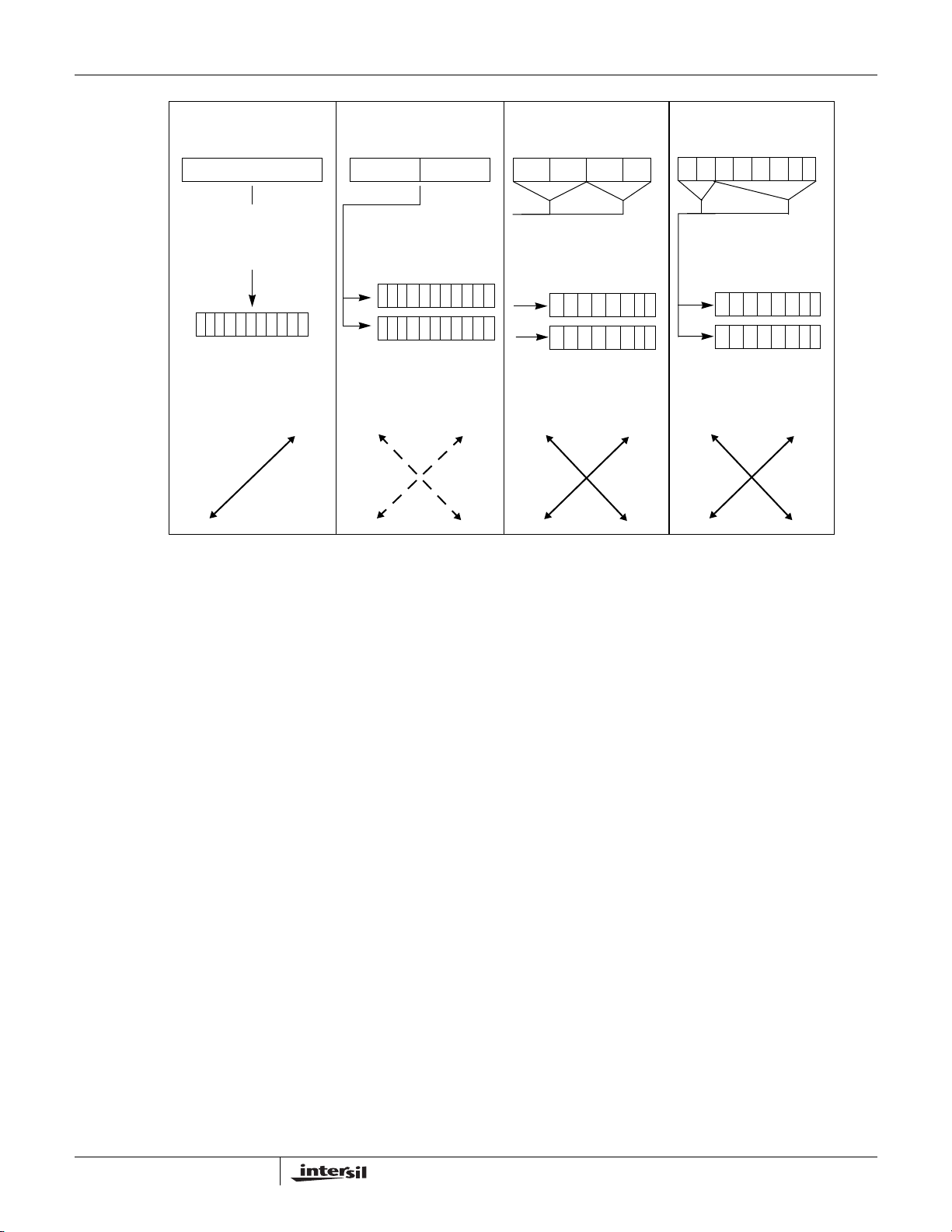
For the 1 and 2Mbps modes, the transmitter accepts data
from the external source, scrambles it, differentially encodes
it as either DBPSK or DQPSK, and spreads it with the BPSK
PN sequence. The baseband digital signals are then output
to the external IF modulator.
For the CCK modes, the transmitter inputs the data and
partitions it into nibbles (4 bits) or bytes (8 bits). At 5.5Mbps,
it uses two of those bits to select one of 4 complex spread
sequences from a table of CCK sequences and then QPSK
modulates that symbol with the remaining 2 bits. Thus, there
are 4 possible spread sequences to send at four possible
carrier phases, but only one is sent. This sequence is then
modulated on the I and Q outputs. The initial phase
reference for the data portion of the packet is the phase of
the last bit of the header. At 11Mbps, one byte is used as
above where 6 bits are used to select one of 64 spread
sequences for a symbol and the other 2 are used to QPSK
modulate that symbol. Thus, the total possible number of
combinations of sequence and carrier phases is 256. Of
these only one is sent.
The bit rate Table 3 shows examples of the bit rates and the
symbol rates and Figure 7 shows the modulation schemes.
The modulator is completely independent from the
demodulator, allowing the PRISM baseband processor to be
used in full duplex operation.
Header/Packet Description
The HFA3861B is designed to handle packetized Direct
Sequence Spread Spectrum (DSSS) data transmissions.
The HFA3861B generates its own preamble and header
information. It uses two packet preamble and header
configurations. The first is backwards compatible with the
existing IEEE 802.11-1997 1 and 2Mbps modes and the
second is the optional shortened mode which maximizes
throughput at the expense of compatibility with legacy
equipment.
In the long preamble mode, the device uses a
synchronization preamble of 128 symbols along with a
header that includes four fields. The preamble is all 1's
(before entering the scrambler) plus a start frame delimiter
(SFD). The actual transmitted pattern of the preamble is
randomized by the scrambler. The preamble is always
transmitted as a DBPSK waveform (1Mbps). The duration of
the long preamble and header is 192
In the short preamble mode, the modem uses a
synchronization field of 56 zero symbols along with an SFD
transmitted at 1Mbps. The short header is transmitted at
2Mbps. The synchronization preamble is all 0’s to distinguish
it from the long header mode and the short preamble SFD is
the time reverse of the long preamble SFD. The duration of
the short preamble and header is 96
µ s.
µ s.

HFA3861B
10
Start Frame Delimiter (SFD) Field (16 Bits) - This field is
used to establish the link frame timing. The HFA3861B will
not declare a valid data packet, even if it PN acquires, unless
it detects the SFD. The HFA3861B receiver is programmed
to time out searching for the SFD via CR 10 BITS 4 and 5.
The timer starts counting the moment that initial PN
synchronization has been established on the preamble.
The four fields for the header shown in Figure 8 are:
Signal Field (8 Bits) -
This field indicates what data rate the
data packet that follows the header will be. The HFA3861B
receiver looks at the signal field to determine whether it
needs to switch from DBPSK demodulation into DQPSK, or
CCK demodulation at the end of the preamble and header
fields.
Service Field (8 Bits) -
The MSB of this field is used to
indicate the correct length when the length field value is
ambiguous at 11Mbps. See IEEE STD 802.11 for definition
of the other bits. Bit 2 is used by the HFA3861B. To indicate
that the carrier reference and the bit timing references are
derived from the same oscillator.
Length Field (16 Bits) -
This field indicates the number of
microseconds it will take to transmit the payload data
(PSDU). The external controller (MAC) will check the length
field in determining when it needs to de-assert RX_PE.
CCITT - CRC 16 Field (16 Bits) -
This field includes the
16-bit CCITT - CRC 16 calculation of the three header fields.
This value is compared with the CCITT - CRC 16 code
calculated at the receiver. The HFA3861B receiver will
indicate a CCITT - CRC 16 error via CR24 bit 2 and will
lower MD_RDY and reset the receiver to the acquisition
mode if there is an error.
The CRC or cyclic Redundancy Check is a CCITT CRC-16
FCS (frame check sequence). It is the ones compliment of
the remainder generated by the modulo 2 division of the
protected bits by the polynomial:
16
12
x
+ x
+ x
5
+ 1
The protected bits are processed in transmit order. All CRC
calculations are made ahead of data scrambling. A shift
register with two taps is used for the calculation. It is preset
to all ones and then the protected fields are shifted through
the register. The output is then complemented and the
residual shifted out MSB first.
The following Configuration Registers (CR) are used to
program the preamble/header functions, more programming
details about these registers can be found in the Control
Registers section of this document:
CR 4 -
Defines the preamble length minus the SFD in
symbols. The 802.11 protocol requires a setting of
128d = 80h for the mandatory long preamble and 56d = 38h
for the optional short preamble.
CR 10 Bits 4, 5 -
Define the length of time that the
demodulator searches for the SFD before returning to
acquisition.
CR 5 Bits 0, 1 -
These bits of the register set the Signal field
to indicate what modulation is to be used for the data portion
of the packet.
CR 6 -
The value to be used in the Service field.
CR 7 and 8 -
Defines the value of the transmit data length
field. This value includes all symbols following the last
header field symbol and is in microseconds required to
transmit the data at the chosen data rate.
The packet consists of the preamble, header and MAC
protocol data unit (MPDU). The data is transmitted exactly
as received from the control processor. Some dummy bits
will be appended to the end of the packet to insure an
orderly shutdown of the transmitter. This prevents spectrum
splatter. At the end of a packet, the external controller is
expected to de-assert the TX_PE line to shut the
transmitter down. Set the scrambler CR36E37 seed valve
for the transmitter.
Scrambler and Data Encoder Description
The modulator has a data scrambler that implements the
scrambling algorithm specified in the IEEE 802.11 standard.
This scrambler is used for the preamble, header, and data in
all modes. The data scrambler is a self synchronizing circuit.
It consists of a 7-bit shift register with feedback from
specified taps of the register. Both transmitter and receiver
use the same scrambling algorithm. The scrambler can be
disabled by setting CR32 bit 2 to 1.
NOTE: Be advised that the IEEE 802.11 compliant scrambler in the
HFA3861B has the property that it can lock up (stop scrambling) on
random data followed by repetitive bit patterns. The probability of this
happening is 1/128. The patterns that have been identified are all
zeros, all ones, repeated 10s, repeated 1100s, and repeated
111000s. Any break in the repetitive pattern will restart the scrambler.
To insure that this does not cause any problem, the CCK waveform
uses a ping pong differential coding scheme that breaks up repetitive
0s patterns.
PREAMBLE (SYNC)
128/56 BITS
PREAMBLE
SFD
16 BITS
SIGNAL FIELD
8 BITS
FIGURE 8. 802.11 PREAMBLE/HEADER
SERVICE FIELD
8 BITS
HEADER
LENGTH FIELD
16 BITS
CRC16
16 BITS

ce
j ϕ1ϕ2ϕ3ϕ
4
+++()
e
j ϕ1ϕ3ϕ
4
++()
e
j ϕ1ϕ2ϕ
4
++()
,
e
j ϕ1ϕ4+()ej ϕ1ϕ2ϕ
3
++()
e
j ϕ1ϕ3+() ej ϕ1ϕ2+()ejϕ
1
,–,,,–
,,
=
HFA3861B
11
Scrambling is done by a division using a prescribed
polynomial as shown in Figure 9. A shift register holds the
last quotient and the output is the exclusive-or of the data
and the sum of taps in the shift register. The taps are
programmable. The transmit scrambler seed for the long
preamble or for the short preamble can be set with CR36 or
CR37.
SERIAL
Z-5 Z-6 Z
DATA OUT
-7
SERIAL DATA
IN
XOR
Z-1 Z-2 Z-3 Z
FIGURE 9. SCRAMBLING PROCESS
-4
XOR
For the 1Mbps DBPSK data rates and for the header in all
rates, the data coder implements the desired DBPSK coding
by differential encoding the serial data from the scrambler
and driving both the I and Q output channels together. For
the 2Mbps DQPSK data rate, the data coder implements the
desired coding as shown in the DQPSK Data Encoder table.
This coding scheme results from differential coding of dibits
(2 bits). Vector rotation is counterclockwise although bits 6
and 7 of configuration register CR 1 can be used to reverse
the rotation sense of the TX or RX signal if desired.
TABLE 4. DQPSK DATA ENCODER
DIBIT PATTERN (d0, d1)
PHASE SHIFT
000
+90 01
+180 11
d0 IS FIRST IN TIME
For the 2Mbps DQPSK mode, the serial data is formed into
dibits or bit pairs in the differential encoder as detailed
above. One of the bits from the differential encoder goes to
the I Channel and the other to the Q Channel. The I and Q
Channels are then both multiplied with the 11-bit Barker
word at the spread rate. This forms QPSK modulation at the
symbol rate with BPSK modulation at the spread rate.
Transmit Filter Description
To minimize the requirements on the analog transmit
filtering, the transmit section shown in Figure 11 has an
output digital filter. This filter is a Finite Impulse Response
(FIR) style filter whose shape is set by tap coefficients. This
filter shapes the spectrum to meet the radio spectral mask
requirements while minimizing the peak to average
amplitude on the output. To meet the particular spread
spectrum processing gain regulatory requirements in Japan,
an extra FIR filter shape has been included that has a wider
main lobe. This increases the 90% power bandwidth from
about 11MHz to 14MHz. It has the unavoidable side effect of
increasing the amplitude modulation, so the available
transmit power is compromised by 2dB when using this filter
(CR 11 bit 5). The receive section Channel Matched Filter
(CMF) is also tailored to match the characteristics of the
transmit filter.
CCK Modulation
The spreading code length is 8 and based on
complementary codes. The chipping rate is 11Mchip/s and
the symbol duration is exactly 8 complex chips long. The
following formula is used to derive the CCK code words that
are used for spreading both 5.5 and 11Mbps:
Spread Spectrum Modulator Description
The modulator is designed to generate DBPSK, DQPSK, and
CCK spread spectrum signals. The modulator is capable of
automatically switching its rate where the preamble is
DBPSK modulated, and the data and/or header are
modulated differently. The modulator can support date rates
of 1, 2, 5.5 and 11Mbps. The programming details to set up
the modulator are given at the introductory paragraph of this
section. The HFA3861B utilizes Quadraphase (I/Q)
modulation at baseband for all modulation modes.
In the 1Mbps DBPSK mode, the I and Q Channels are
connected together and driven with the output of the
scrambler and differential encoder. The I and Q Channels
are then both multiplied with the 11-bit Barker word at the
spread rate. The I and Q signals go to the Quadrature
upconverter (HFA3724) to be modulated onto a carrier.
Thus, the spreading and data modulation are BPSK
modulated onto the carrier.
-90 10
(LSB to MSB), where c is the code word.
The terms:
ϕ
1, ϕ
2, ϕ
3, and ϕ
4 are defined below for
5.5Mbps and 11Mbps.
This formula creates 8 complex chips (LSB to MSB) that are
transmitted LSB first. The coding is a form of the generalized
Hadamard transform encoding where
chips,
ϕ 2 is added to all odd code chips, ϕ 3 is added to all
odd pairs of code chips and
ϕ
4 is added to all odd quads of
ϕ
1 is added to all code
code chips.
The phases
ϕ 1 modify the phase of all code chips of the
sequence and are DQPSK encoded for 5.5 and 11Mbps.
This will take the form of rotating the whole symbol by the
appropriate amount relative to the phase of the preceding
symbol. Note that the last chip of the symbol defined above
is the chip that indicates the symbol’s phase.
 Loading...