Intersil Corporation HFA3766 Datasheet

HFA3766
PRELIMINARY
400MHz AGC Quadrature IF
Modulator/Demodulator
™
The HFA3766 is a highly integrated
baseband converter for quadrature
modulation applications. It features all
the necessary blocks for baseband
modulation and demodulation of I and
Q signals. It has a twostageintegratedAGCIFamplifierwith
82dB of voltage gain and 76dB of gain control range.
Baseband antialiasing is integrated into the design. Four
filter bandwidths are programmable via a two bit digital
control interface. In addition, these filters are continuously
tunable over a ±20% frequency range via one external
resistor. For baseband modulation digital I and Q data are
delivered to the transmit section. To achieve broadband
operation, the Local Oscillator frequency input is required
to be twice the desired frequency of modulation and
demodulation. A selectable buffered divide by 2 LO output
and a stable reference voltage are provided for convenience
of the user. The device is housed in a thin 80 lead TQFP
package well suited for PCMCIA board applications.
January 1999 File Number 4328.1
Features
• Integrates all IF Transmit and AGC Receive Functions
• Broad Frequency Range . . . . . . . . . . 10MHz to 400MHz
• I/Q Amplitude and Phase Balance . . . . 0.2dB, 2 Degrees
• 5th Order Programmable
Low Pass Filter. . . . . . . . . . . . . . . . . .2.2MHz to 17.6MHz
• 400MHz AGC Gain Strip . . . . . . . . . . . . . . . . . . . . . 82dB
• AGC Range . . . . . . . . . . . . . . . . . . . . . . . . . . . . . . . 75dB
• Low LO Drive Level . . . . . . . . . . . . . . . . . . . . . . . -15dBm
• Fast AGC Switching . . . . . . . . . . . . . . . . . . . . . . . . . . 1µs
• Fast Transmit-Receive Switching . . . . . . . . . . . . . . . . . . . 1µs
• Power Management/Standby Mode
• Single Supply 3.0V Operation
• Wireless Local Loop
• Wireless Local Area Networks
• PCMCIA Wireless Transceivers
• ISM Systems
• CDMA Radios
• PCS/Wireless PBX
Ordering Information
TEMP.
PART NUMBER
HFA3766IN -40 to 85 80 Ld TQFP Q80.14x14
HFA3766IN96 -40 to 85 Tape and Reel
RANGE (oC) PACKAGE PKG. NO.
Simplified
AGC_SEl
AGC1_IN
AGC1_VAGC
AGC2_VAGC
LO_IN
LO_OUT
LO_GND
MOD_TX_IF_OUT
1
AGC1_OUT
AGC2_IN
2V REF
2V REF
CAUTION: These devices are sensitive to electrostatic discharge; follow proper IC Handling Procedures.
AGC2_OUT
∑
DEMOD_IFIN
÷2
0o/90
DEMOD_RXQ
I
M
U
o
X
Q
LPF_TXI
MOD_TXI
LPF_TXQ
MOD_TXQ
www.intersil.com or 407-727-9207 | Copyright © Intersil Corporation 1999
LPF_SEL0
LPF_SEL1
LPF_TUNE_0
LPF_RXI_OUT
LPF_RXQ _OUT
M
U
X
PRISM and PRISM logo are trademarks of Intersil Corporation.
LPF_TXI_IN
LPF_TXQ_IN
TX D OR A
LPF_TUNE_1
LPF_RXI
LPF_RXQ
DEMOD_RXI

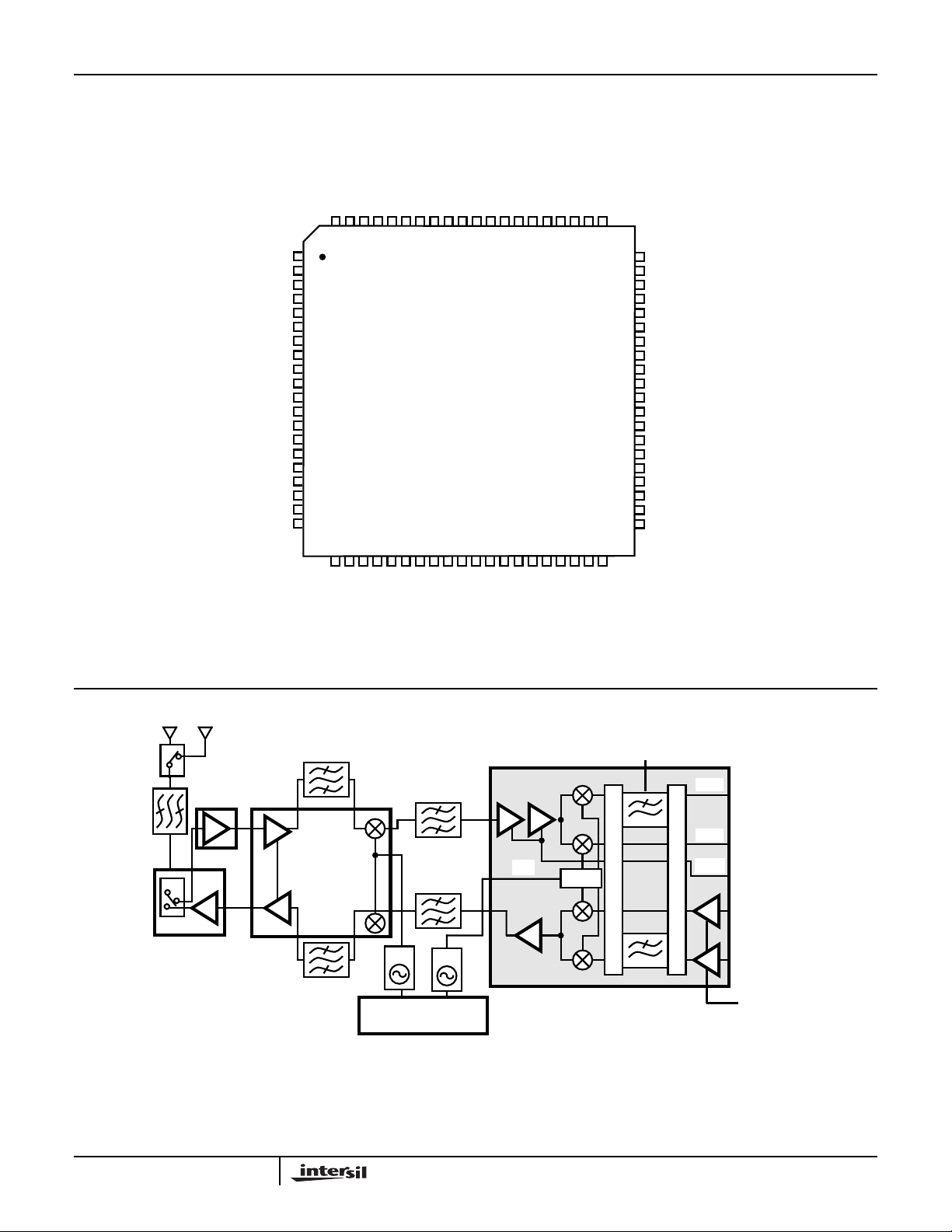
Pinout
HFA3766
80 LEAD TQFP
TOP VIEW
AGC
AGC1_BYP+
AGC1_IN+
GND
AGC1_SEL
AGC1_IN-
AGC1_BYP-
GND
GND
LPF_V
CC
2V REF
LPF_BYP
LPF_TXI_IN
LPF_TXQ_IN
LPF_RXI_OUT
LPF_RXQ_OUT
LPF_SEL1
LPF_SEL0
LPF_TUNE1
LPF_TUNE0
TX D OR A
AGC1_VCCAGC1_PE
AGC1_OUT+
LPF_TXI-
LPF_TXI+
LPF_TXQ-
LPF_TXQ+
AGC1_OUT-
AGC1_VCCGND
LPF_RXQ-
GND
GND
GND
GND
LPF_RXI-
LPF_RXI+
LPF_RXQ+
GND
GND
AGC1_V
GND
80
1
2
3
4
5
6
7
8
9
10
11
12
13
14
15
16
17
18
19
20
2122 2324 25 2627 282930 313233 3435 36
LPF_TX_PE
LPF_RX_PE
GND
GND
GND
AGC2_BYP-
AGC2_IN-
64656667686970717273747576777879
3738 3940
MOD_TXI+
DEMOD_RXI-
DEMOD_RXI+
DEMOD_RXQ-
DEMOD_RXQ+
GND
AGC2_IN+
6362 61
MOD_TXI-
MOD_TXQ+
AGC2_BYP+
60
59
58
57
56
55
54
53
52
51
50
49
48
47
46
45
44
43
42
41
MOD_TXQ-
AGC2_V
AGC
GND
AGC2_V
CC
AGC2_PE
AGC2_OUT+
AGC2_OUTAGC2_V
CC
GND
GND
GND
LO_GND
DEMOD_IFINDEMOD_IFIN+
MOD_V
CC
LO_OUT
MOD_V
CC
LO_IN
DEMOD_RX_PE
MOD_TX_IF_OUT
MOD_TX_PE
Typical Application Diagram
HFA3424(NOTE)
(FILE# 4131)
HFA3624
RF/IF
CONVERTER
(FILE# 4066)
RFPA
HFA3925
(FILE# 4132)
Foradditionalinformation on the PRISM™ FullDuplexRadio
Chip Set, call (407) 724-7800 toaccessIntersil’s AnswerFAX
system. When prompted, key in the four-digit document
number (File #) of the data sheets you wish to receive.
VCO
DUAL SYNTHESIZER
HFA3524 (FILE# 4062)
VCO
HFA3766
(FILE# 4328)
÷ 2
QUAD IF MODEM
0o/90
TUNE/SELECT
M
o
U
X
RXI
I
M
RXQ
U
X
VAGC
M
U
X
Q
PRISM™ CHIP SET FILE #4063
TX D OR A
The four-digit file numbers are shown in Typical Application
Diagram, and correspond to the appropriate circuit.
2

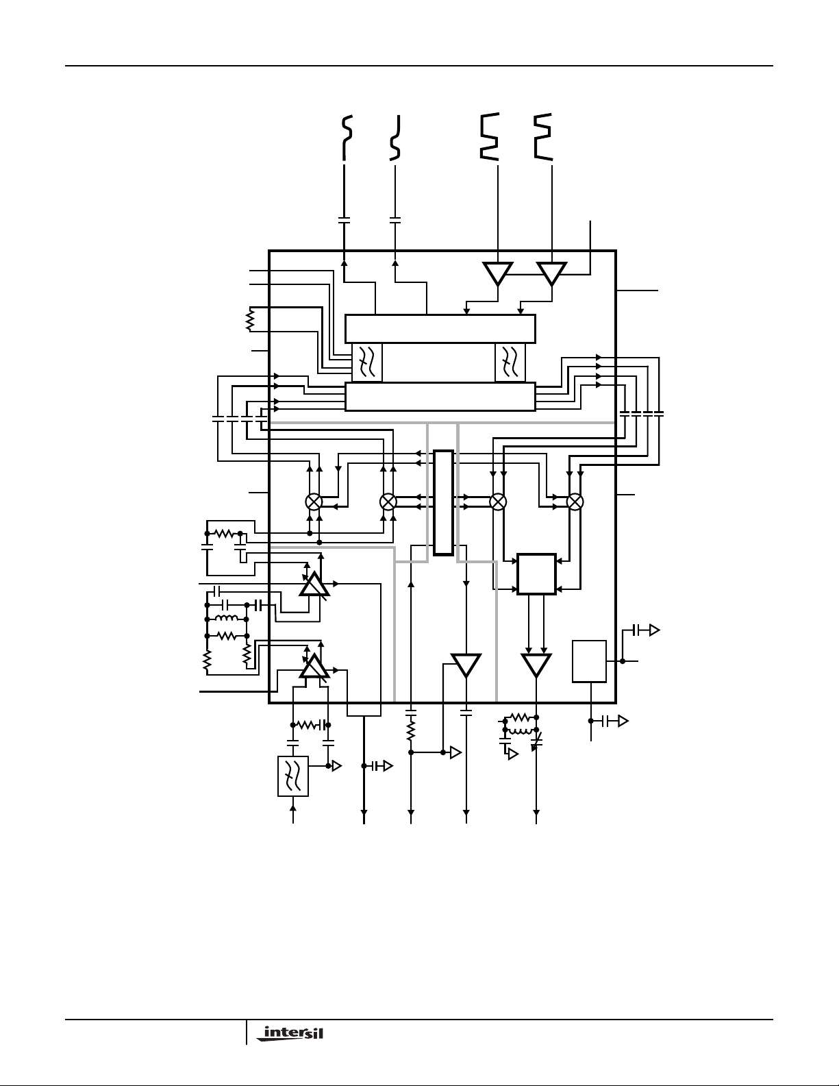
Block Diagram
LPF_RXI -
LPF_RXI +
LPF_RXQ +
LPF_RXQ -
DEMOD_RXQ -
DEMOD_RXQ +
DEMOD_RXI -
DEMOD_RXI +
DEDEMOD_IFIN+
DEMOD_IFIN -
AGC2_OUT -
AGC2_OUT +
AGC2_PE
AGC2_IN+
AGC2_IN-
AGC1_OUT -
AGC1_OUT +
AGC1_PE
LPF_SEL1
LPF_SEL0
LPF_TUNE0
LPF_TUNE1
LPF_RX_PE
DEMOD_RX_PE
1000p
33p
10nH
NO FIT
56
56
1000p
DOWN CONV
IF
IF
HFA3766
LPF_RXI_OUT
LPF_RXQ_OUT
-
I
TX D OR A
LPF_TXI_IN
MUX
Q
MUX
o
/90
o
0
÷2
AGC
UP CONVERTER
LPF_TXQ_IN
∑
MUX_LPF
2V
REF
LPF_TX_PE
LPF_TXQ LPF_TXQ +
LPF_TXI LPF_TXI +
MOD _TXI +
MOD _TXI MOD _TXQ +
MOD _TXQ -
MOD_TX_PE
2V REF
AGC1_IN+
SAW
IF
IN
NOTE: VCC, GND and Bypass capacitors not shown.
3
AGC
AGC1_IN-
AGC1_V
VAGC
AGC
AGC2_V
LO_IN
(2XLO)
LO_GND
50Ω
LO_OUT
CC
V
LPF_BYP
1.25V
IF_OUT
MOD_TX

HFA3766
Pin Descriptions
PIN SYMBOL DESCRIPTION
1 AGC1_BYP+ DC feedback pin for AGC amplifier 1. Requires good decoupling and minimum wire length to a solid signal
ground.
2 AGC1_IN+ Non-inverting analog input of AGC amplifier 1.
3 GND Ground. Connect to a solid ground plane.
4 AGC_SEL This pin selects either differential or single ended input configuration for the first stage AGC. Ground this pin for
differential input configuration. Leave it floating for single ended input configuration.
5 AGC1_IN- Inverting analog input of AGC amplifier 1.
6 AGC1_BYP- DC feedback pin for AGC amplifier 1. Requires good decoupling and minimum wire length to a solid signal
ground.
7, 8 GND Ground. Connect to a solid ground plane.
9 LPF_V
10 2V REF Stable 2V reference voltage output for external applications. Loading must be higher than 10kΩ. A bypass
11 LPF_BYP Internal reference bypass pin. This is the common voltage (VCM) used for the LPF digital thresholds. Requires
12 LPF_TXI_IN Low pass filter in phase (I) channel transmit input. Conventional or attenuated direct coupling is required for
13 LPF_TXQ_IN Low pass filter quadrature (Q) channel transmit input. Conventional or attenuated direct coupling is required for
14 LPF_RX_I Low pass filter in phase (I) channel receive output. Requires AC coupling.
15 LPF_RX_Q Low pass filter quadrature (Q) channel receive output. Requires AC coupling.
16 LPF_SEL1 Digitalcontrolinput pins.Selectsfour programmedcut off frequenciesfor thereceive channel. Tuning speedfrom
17 LPF_SEL0
18 LPF_TUNE1 These two pins are used to fine tune the Low pass filter cutoff frequency. A resistor connected between the two
19 LPF_TUNE0
20 TXD or TXA Selects between digital or analog signals. Tie to GND for digital. Tie to VCC for analog.
21 LPF_RX_PE Digital input control pin to enable the LPF receive mode of operation. Enable logic level is High.
CC
Supply pin for the Low pass filter. Use high quality decoupling capacitors right at the pin.
capacitor of at least 0.1µF is required.
0.1µF decoupling capacitor.
digital inputs.
digital inputs
one cutoff to another is less than 1µs.
SEL1 SEL0 CUTOFF FREQUENCY SEl1 SEl0 CUTOFF FREQUENCY
LO LO 2.2MHz HI LO 8.8MHz
LO HI 4.4MHz HI HI 17.6MHz
pins (R
specifications.
) will fine tune both transmit and receive filters. Refer to the tuning equation in the LPF AC
TUNE
22 LPF_TX_PE Digital input control pin to enable the LPF transmit mode of operation. Enable logic level is High.
23 LPF_TXQ- Negative output of the transmit Low pass filter, quadrature channel. ACcoupling is required. Normally connects
to the inverting input of the quadrature Modulator (Mod_TXQ-), pin 40.
24 LPF_TXQ+ Positive output of the transmit Low pass filter, quadrature channel. AC coupling is required. Normally connects
to the non inverting input of the quadrature Modulator (Mod_TXQ+), pin 39.
25 LPF_TXI- Negative output of the transmit Low pass filter, in phase channel. ACcouplingisrequired.Normally connects to
the inverting input of the in phase Modulator (Mod_TXI-), pin 38.
26 LPF_TXI+ Positive output of the transmit Low pass filter, in phase channel. AC coupling is required. Normally connects to
the non inverting input of the in phase Modulator (Mod_TXI+), pin 37.
27 LPF_RXQ- Low pass filter inverting input of the receive quadrature channel. AC coupling is required. This input is normally
coupled to the negative output of the quadrature demodulator (Mod_RXQ-), pin 36.
4
 Loading...