

TM
HFA3761
Data Sheet July 1999 File Number 4236.4
400MHz AGC and Quadrature IF
Demodulator
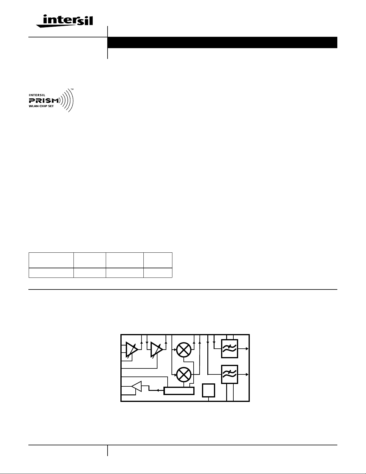
The HFA3761 is a highly integrated
baseband converter for quadrature
demodulation applications. The
HFA3761 400MHz AGC and
quadrature IF demodulator is one of the
seven chips in the PRISM® full duplex chip set (see Typical
Application Diagram). It features all the necessary blocks for
baseband demodulation of I and Q signals. It has a two
stage integrated AGC IF amplifier with 82dB of voltage gain
and 76dB of gain control range. Baseband antialiasing and
shaping filters are integrated in the design. Four filter
bandwidths are programmable via a two bit digital control
interface. In addition, these filters are continuously tunable
over a ±20% frequency range via one external resistor. To
achieve broadband operation, the Local Oscillator
frequency input is required to be twice the desired
frequency of demodulation. A selectable buffered divide by
2 LO output and a stable reference voltage are provided for
convenience of the user. The device is housed in a thin 80
lead TQFP package well suited for PCMCIA board
applications.
Features
• Integrates all IF and AGC Receive Functions
• Broad Frequency Range . . . . . . . . . . 10MHz to 400MHz
• I/Q Amplitude and Phase Balance . . . . 0.2dB, 2 Degrees
• 5th Order Programmable
Low Pass Filter. . . . . . . . . . . . . . . . . 2.2MHz to 17.6MHz
• 400MHz AGC Gain Strip . . . . . . . . . . . . . . . . . . . . . 82dB
• AGC Range . . . . . . . . . . . . . . . . . . . . . . . . . . . . . . . 75dB
• Low LO Drive Level . . . . . . . . . . . . . . . . . . . . . . . -15dBm
• Fast AGC Switching . . . . . . . . . . . . . . . . . . . . . . . . . . 1µs
• Power Management/Standby Mode
• Single Supply 2.7V to 5.5V Operation
Applications
• Wireless Local Loop
• Wireless Local Area Networks
• PCMCIA Wireless Transceivers
• ISM Systems
Ordering Information
TEMP.
PART NUMBER
HFA3761IN -40 to 85 80 Ld TQFP Q80.14x14
RANGE (oC) PACKAGE PKG. NO.
Simplified Block Diagram
AGC1_OUT
AGC2_IN
AGC_SEL
AGC1_IN
AGC1_V
AGC
AGC2_V
AGC
DEMOD_LO_IN
DEMOD_LO_OUT
LO_GND
AGC2_OUT
DEMOD_IF_IN
÷2
0o/90
• CDMA Radios
• PCS/Wireless PBX
LPF_TUNE_1
LPF_RX_I
LPF_RX_Q
DEMOD_RX_I
DEMOD_RX_Q
I
Q
2V
o
REF
2V REF
LPF_SEL0
LPF_TUNE_0
LPF_RXI_OUT
LPF_RXQ _OUT
LPF_SEL1
4-1
1-888-INTERSIL or 321-724-7143 | Intersil and Design is a trademark of Intersil Corporation. | Copyright © Intersil Corporation 2000
CAUTION: These devices are sensitive to electrostatic discharge; follow proper IC Handling Procedures.
PRISM® is a registered trademark of Intersil Corporation. PRISM logo is a trademark of Intersil Corporation.
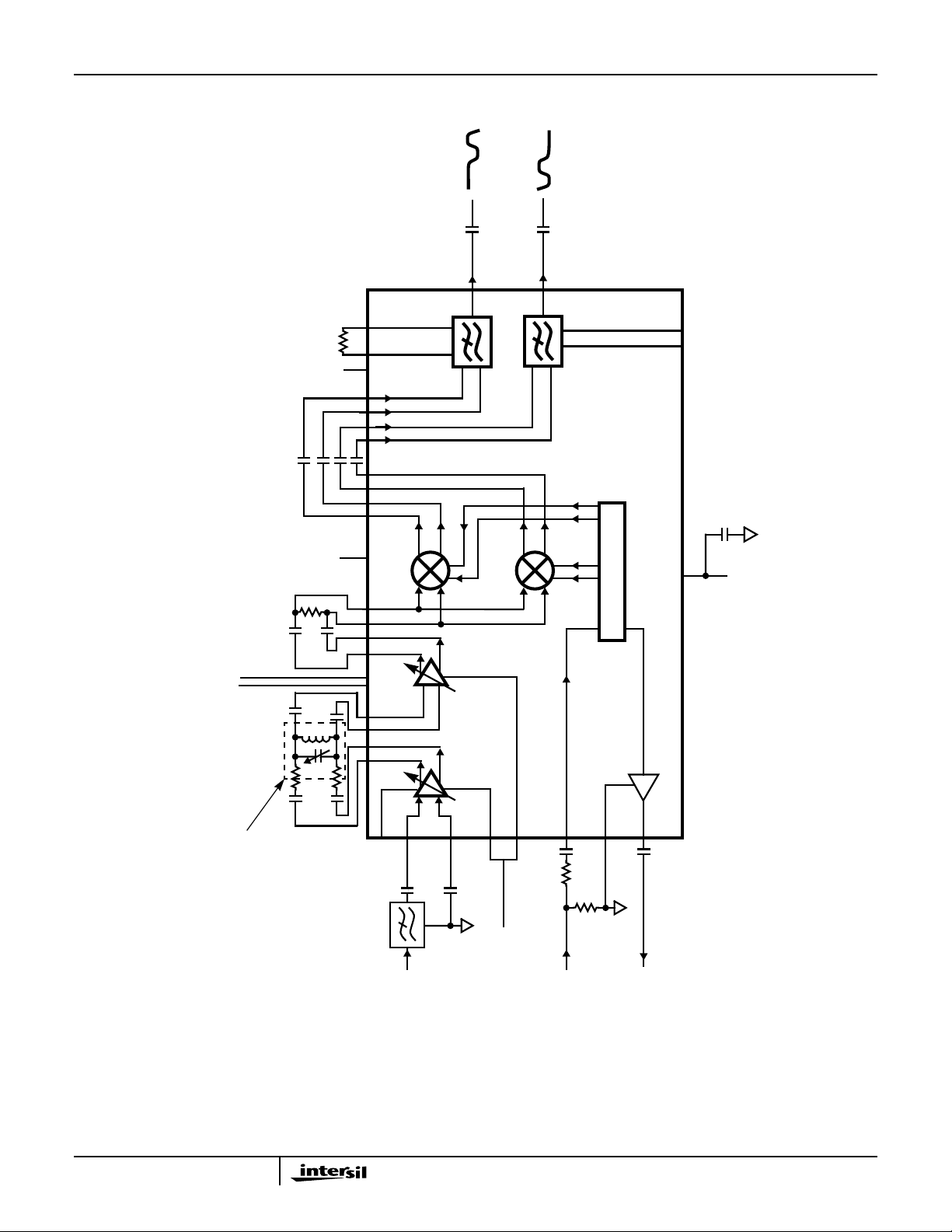
Pinout
HFA3761
80 LEAD TQFP
TOP VIEW
AGC1_BYP+
AGC1_IN+
GND
AGC_SEL
AGC1_IN-
AGC1_BYP-
GND
GND
LPF_V
CC
2V REF
LPF_BYP
NC
LPF_RXI_OUT
LPF_RXQ_OUT
NC
LPF_SEL1
LPF_SEL0
LPF_TUNE1
LPF_TUNE0
GND
CC
AGC
GND
AGC1_V
AGC1_V
80
1
2
3
4
5
6
7
8
9
10
11
12
13
14
15
16
17
18
19
20
2122 2324 2526 27 2829 3031 323334 3536
NC
GND
LPF_RX_PE
AGC1_PE
AGC1_OUT-
AGC1_OUT+
NCNCNC
CC
GND
GND
AGC1_V
LPF_RXI-
LPF_RXQ-
LPF_RXQ+
GND
GND
GND
GND
GND
LPF_RXI+
AGC2_BYP-
GND
GND
GND
AGC2_IN-
64656667686970717273747576777879
3738 3940
NCNCNC
DEMOD_RXI-
DEMOD_RXI+
DEMOD_RXQ-
DEMOD_RXQ+
AGC2_IN+
GND
6362 61
AGC2_BYP+
AGC2_V
60
GND
59
AGC2_V
58
AGC2_PE
57
AGC2_OUT+
56
AGC2_OUT-
55
54
AGC2_V
53
GND
GND
52
GND
51
LO_GND
50
DEMOD_IFIN-
49
DEMOD_IFIN+
48
DEMOD_V
47
46
LO_OUT
45
DEMOD_V
44
LO_IN
43
DEMOD_RX_PE
DEMOD_V
42
41
GND
NC
AGC
CC
CC
CC
CC
CC
Typical Full Duplex Application Diagram
PRISM FULL DUPLEX CHIP SET
HFA3424/21
(File #4131)
D
U
P
L
E
X
E
R
LNA BPF
HFA3925
(File #4132)
PA BPF
HFA3524
(File #4062)
HFA3524
(File #4062)
For additional information on the PRISM Full Duplex Radio
Chip Set, call (321) 724-7800 to access Intersil’ AnswerFAX
system. When prompted, key in the four-digit document
number (File #) of the data sheets you wish to receive.
HFA3661
(File #4240)
LNA
SYNTHESIZER
SYNTHESIZER
AGC
HFA3663 (File #4241)
HFA3664 (File #4242)
RF/IF
CONVERTER
RF LO1
RF LO2
IF/RF
CONVERTER
FILTER
IF LO1
IF LO2
HFA3761 (File #4236)
IF AGC
AGC
QMODEM
LPF
LPF
HFA3763
(File #4237)
LPF
QMODEM
LPF
A/D
BASEBAND
D/A
OPTIONAL WHEN IN
ANALOG MODE
PRISM FULL DUPLEX RADIO
CHIP SET, FILE #4238
The four-digit file numbers are shown in Typical Application
Diagram, and correspond to the appropriate circuit.
4-2
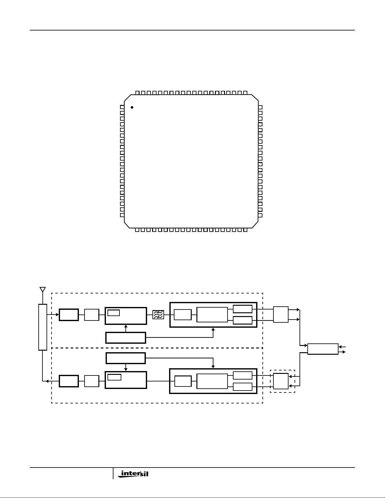
Block Diagram
HFA3761
DEMOD_RX Q -
DEMOD_RX Q +
DEMOD_RX I -
DEMOD_RX I +
DEMOD_IF_IN +
DEMOD_IF_IN -
AGC2_OUT -
AGC2_OUT +
AGC2_PE
AGC1_PE
AGC2_IN+
AGC2_IN-
AGC1_OUT -
AGC1_OUT +
LPF_TUNE0
LPF_TUNE1
LPF_RX PE
LPF_RX I -
LPF_RX I +
LPF_RX Q +
LPF_RX Q -
DEMOD_RX PE
DOWN CONV
LPF_RXI_OUT
IF
LPF_RXQ_OUT
LPF_SEL1
LPF_SEL0
o
/90
o
0
2V REF
÷2
OPTIONAL FILTER
NOTE: VCC, GND and Bypass capacitors not shown.
4-3
AGC_SEL
SAW
IF
IF
AGC1_IN+
IN
AGC
AGC1_IN-
AGC1_V
AGC
AGC2_V
AGC CTRL
LO_GND
(2XLO)
DEMOD_LO_IN
50Ω
DEMOD_LO_OUT

HFA3761
Pin Descriptions
PIN SYMBOL DESCRIPTION
1 AGC1_BYP+ DCfeedback pinforAGC amplifier 1. Requiresgooddecouplingand minimum wire length to a solid signalground.
2 AGC1_In+ Non-inverting analog input of AGC amplifier 1.
3 GND Ground. Connect to a solid ground plane.
4 AGC_Sel This pin selects either differential or single ended input configuration for the first stage AGC. Ground this pin for
differential input configuration. Leave it floating for single ended input configuration.
5, AGC1_In- Inverting analog input of AGC amplifier 1.
6, AGC1_BYP- DC feedbackpinfor AGC amplifier 1.Requiresgooddecoupling and minimum wire length to asolidsignalground.
7, 8 GND Ground. Connect to a solid ground plane.
9 LPF_V
10 2V REF Stable 2V reference voltage output for external applications. Loading must be higher than 10kΩ. A bypass
11 LPF_BYP Internal reference bypass pin. This is the common voltage (VCM) used for the LPF digital thresholds. Requires
12 NC Connected internally for test purposes. Pin must be left floating.
13 NC Connected internally for test purposes. Pin must be left floating.
14 LPF_RXI_Out Low pass filter in phase (I) channel receive output. Requires AC coupling.
15 LPF_RXQ_Out Low pass filter quadrature (Q) channel receive output. Requires AC coupling.
16 LPF_Sel1 Digital control input pins. Selects four programed cut off frequencies for the receive channel. Tuning speed from
17 LPF_Sel0
18 LPF_Tune1 These two pins are used to fine tune the Low pass filter cutoff frequency. A resistor connected between the two
19 LPF_Tune0
20 GND Ground. Connect to a solid ground plane.
21 LPF_RX_PE Digital input control pin to enable the LPF receive mode of operation. Enable logic level is High.
22 GND Ground. Connect to a solid ground plane.
23 NC Connected internally for test purposes. Pin must be left floating.
24 NC Connected internally for test purposes. Pin must be left floating.
25 NC Connected internally for test purposes. Pin must be left floating.
26 NC Connected internally for test purposes. Pin must be left floating.
27 LPF_RXQ- Low pass filter inverting input of the receive quadrature channel. AC coupling is required. This input is normally
28 LPF_RXQ+ Low pass filter non inverting input of the receive quadrature channel. AC coupling is required. This input is
29 LPF_RXI- Low pass filter inverting input of the receive in phase channel. AC coupling is required. This input is normally
30 LPF_RXI+ Low pass filter non inverting input of the receive in phase channel. AC coupling is required. This input is normally
31, 32 GND Ground. Connect to a solid ground plane.
33 DEMOD_RXI+ Inphasedemodulatorpositiveoutput.ACcoupling is required. Normally connects to the non inverting input of the
34 DEMOD_RXI- In phase demodulator negative output. AC coupling is required. Normally connects to the inverting input of the
Supply pin for the Low pass filter. Use high quality decoupling capacitors right at the pin.
CC
capacitor of at least 0.1µF is required.
0.1µF decoupling capacitor.
one cutoff to another is less than 1µs.
SEL1 SEL0 CUTOFF FREQUENCY SEL1 SEL0 CUTOFF FREQUENCY
LO LO 2.2MHz HI LO 8.8MHz
LO HI 4.4MHz HI HI 17.6MHz
pins (R
specifications.
coupled to the negative output of the quadrature demodulator (Mod_RXQ-), pin 36.
normally coupled to the positive output of the quadrature demodulator (Mod_RXQ+), pin 35.
coupled to the negative output of the in phase demodulator (Mod_RXI-), pin 34.
coupled to the positive output of the in phase demodulator (DEMOD_RXI-), pin 33.
Low pass filter (LPF_RXI+), pin 30.
Low pass filter (LPF_RXI-), pin 29.
) will fine tune both transmit and receive filters. Refer to the tuning equation in the LPF AC
TUNE
4-4

HFA3761
Pin Descriptions (Continued)
PIN SYMBOL DESCRIPTION
35 DEMOD_RXQ+ Quadrature demodulator positive output. AC coupling is required. Normally connects to the non inverting input of
the Low pass filter (LPF_RXQ+), pin 28.
36 DEMOD_RXQ- Quadrature demodulator negative output. AC coupling is required. Normally connects to the inverting input of the
Low pass filter (LPF_RXQ+), pin 27.
37 NC Connected internally for test purposes. Pin must be left floating.
38 NC Connected internally for test purposes. Pin must be left floating.
39 NC Connected internally for test purposes. Pin must be left floating.
40 NC Connected internally for test purposes. Pin must be left floating.
41 GND Ground. Connect to a solid ground plane.
42 DEMOD_V
43 DEM_RX_PE Digital input control to enable the demodulator section. Enable logic level is High.
44 DEM_LO_In
(2XLO)
45 DEMOD_V
46 DEM_LO_Out Divide by 2 buffered output reference from “DEMOD_LO_in” input. Used for external applications where the
47 DEMOD_V
48 DEMOD_IFIN+ Demodulator, non-inverting input. Requires AC coupling.
49 DEMOD_IFIN- Demodulator, inverting input. Requires AC coupling.
50 LO_GND When grounded, this pin enables the LO buffer (DEMOD_LO_Out). When open (NC) it disables the LO buffer.
51, 52, 53 GND Ground. Connect to a solid ground plane.
54 AGC2_V
55 AGC2_Out- Positive output of AGC amplifier 2. Requires AC coupling.
56 AGC2_Out+ Negative output of AGC amplifier 2. Requires AC coupling.
57 AGC2_PE Digital input control to enable the AGC amplifier 2. Enable logic level is High.
58 AGC2_V
59 GND Ground. Connect to a solid ground plane.
60 AGC2_V
61 AGC2_BYP+ DC feedback pin forAGC amplifier 2. Requires good decouplingandminimumwire length to a solid signal ground.
62 AGC2_In+ Non-inverting analog input of AGC amplifier 2.
63 GND Ground. Connect to a solid ground plane.
64 AGC2_In- Inverting input of AGC amplifier 2.
65 AGC2_BYP- DC feedbackpinfor AGC amplifier2.Requiresgood decoupling and minimum wire length to asolidsignal ground.
66 - 73 GND Ground. Connect to a solid ground plane.
74 AGC1_V
75 AGC1_Out- Negative output of AGC amplifier 1. Requires AC coupling.
76 AGC1_Out+ Positive output of AGC amplifier 1. Requires AC coupling.
77 AGC1_PE Digital input control to enable the AGC amplifier 1. Enable logic level is High.
78 AGC1_V
79 GND Ground. Connect to a solid ground plane.
80 AGC1_V
Supply pin for the Demodulator. Use high quality decoupling capacitors right at the pin.
CC
Single ended local oscillator current input. Frequency of input signal must be twice the required demodulator LO
frequency. Input current is optimum at 200µA
range of power and impedances at this port. Typical input impedance is 130Ω. This pin requires AC coupling.
NOTE: High second harmonic content input waveforms may degrade I/Q phase accuracy.
Supply pin for the Demodulator. Use high quality decoupling capacitors right at the pin.
CC
demodulating carrier reference frequency is required. 50Ω single end driving capability. This output can be
disabled by use of pin 50. AC coupling is required.
Supply pin for the Demodulator. Use high quality decoupling capacitors right at the pin.
CC
Supply pin for the AGC amplifier 2. Use high quality decoupling capacitors right at the pin.
CC
Supply pin for the AGC amplifier 2. Use high quality decoupling capacitors right at the pin.
CC
AGC amplifier 2, AGC control input.
AGC
AGC amplifier 1 supply pin. Use high quality decoupling capacitors right at the pin.
CC
AGC amplifier 1 supply pin. Use high quality decoupling capacitors right at the pin.
CC
AGC amplifier 1, AGC control input.
AGC
. Input matching networks and filters can be designed for a wide
RMS
4-5

HFA3761
Absolute Maximum Ratings Thermal Information
Supply Voltage. . . . . . . . . . . . . . . . . . . . . . . . . . . . . . -0.3V to +6.0V
Voltage on Any Other Pin. . . . . . . . . . . . . . . . . . -0.3V to VCC +0.3V
Operating Conditions
Supply Voltage Range. . . . . . . . . . . . . . . . . . . . . . . . . . . 2.7 to 5.5V
Operating Temperature Range . . . . . . . . . . . . . . -40oC ≤ TA≤ 85oC
CAUTION: Stresses above those listed in “Absolute Maximum Ratings” may cause permanent damage to the device. This is a stress only rating and operation of the
device at these or any other conditions above those indicated in the operational sections of this specification is not implied.
NOTE:
1. θJA is measured with the component mounted on an evaluation PC board in free air.
Thermal Resistance (Typical, Note 1) θJA (oC/W)
TQFP Package. . . . . . . . . . . . . . . . . . . . . . . . . . . . . 75
Package Power Dissipation at 70oC
TQFP Package. . . . . . . . . . . . . . . . . . . . . . . . . . . . . . . . . . . .1.1W
Maximum Junction Temperature (Plastic Package). . . . . . . . .150oC
Maximum Storage Temperature Range. . . . . . . -65oC ≤ TA≤ 150oC
Maximum Lead Temperature (Soldering 10s) . . . . . . . . . . . . .300oC
(TQFP - Lead Tips Only)
Cascaded DC Electrical Specifications V
PARAMETER
Total Supply Current, at 5.5V A Full - 80 112 mA
Shutdown (Standby) Current at 5.5V A Full - .8 1.5 mA
All Digital Inputs VIH (TTL Threshold for All VCC) A Full 2.0 - V
All Digital Inputs VIL (TTL Threshold for All VCC) A Full -0.2 - 0.8 V
High Level Input Current at 5.5V VCC for pins 16 and 21 with VIN = 2.4V A Full -200 -65 0 µA
High Level Input Current at 5.5V VCC for pins 16 and 21 with VIN = 4.0V A Full -150 -30 0 µA
Low Level Input Current at 5.5V VCC for pins 16 and 21 with VIN = 0.8V A Full -300 -95 0 µA
High Level Input Current at 5.5V VCC for pin 17, with VIN = 2.4V A Full 0 50 200 µA
High Level Input Current at 5.5V VCC for pin 17, with VIN = 4.0V A Full 0 80 300 µA
Low Level Input Current at 5.5V VCC for pin 17, with VIN = 0.8V A Full 0 15 150 µA
High Level Input Current at 5.5V VCC for pin 43 with VIN = 2.4V A Full -20 1 20 µA
High Level Input Current at 5.5V VCC for pin 43 with VIN = 4.0V A Full 0 110 300 µA
Low Level Input Current at 5.5V VCC for pin 43 with VIN = 0.8V A Full -20 .1 20 µA
V
Input for Max Gain (Note 5) A 25 .8 1.1 - V
AGC
V
Input for Min Gain (Note 5) A 25 - 2.1 2.2 V
AGC
V
Control Input Impedance (Per Stage) (Note 3) C 25 - 410 - Ω
AGC
V
Control Input Current (Per Stage) at Max Control Voltage A 25 - .5 2.0 mA
AGC
Full Range AGC Switching Large Signal Recovery (Note 4) B 25 - 400 - ns
Full Range AGC Switching 1dB Settling Time (Note 4) B 25 - 1.5 - µs
Power Down/Up Switching Speed (Note 4) B 25 - 2 - µs
Reference Voltage A Full 1.85 2.0 2.15 V
Reference Voltage Variation Over Temperature B 25 - 800 - µV/oC
Reference Voltage Variation Over Supply Voltage B 25 - 1.6 - mV/V
Reference Voltage Minimum Load Resistance C 25 10 - - kΩ
NOTES:
2. A = Production Tested, B = Based on Characterization, C = By Design.
3. 1.2V reference source in series with 410Ω.
4. Determined by external components.
5. Measured at probe.
= 4.5V to 5.5V, Unless Otherwise Specified
CC
(NOTE 2)
TEST
LEVEL TEMP (oC) MIN TYP MAX UNITS
CC
V
4-6

HFA3761
Cascaded AC Electrical Specifications, Demodulator Chain Performance V
MHz, Unless Otherwise Specified
(NOTE 6)
TEST
PARAMETER
IF Demodulator I and Q Outputs Voltage Swing
(IF input Range of -70 dBm to -30 dBm)
IF Demodulator I and Q Channels Output Drive Capability
(Z
= 50Ω) C
OUT
IF Demodulator I/Q Amplitude Balance, IFin = -70dBm at 50Ω A Full -1.0 0 +1.0 dB
IF Demodulator I/Q Phase Balance, IFin = -70dBm at 50Ω A Full -4.0 0 +4.0 Degrees
IF Demodulator Output, P1dB TBD TBD TBD TBD TBD mV
NOTES:
6. A = Production Tested, B = Based on Characterization, C = By Design.
7. Determined by external components.
MAX
= 10pF, V
OUT
= 500mV
P-P
AC Electrical Specifications, Cascaded AGC Stages Performance V
PARAMETER
Frequency Range (Note 9) B 25 10 - 400 MHz
Voltage Gain at Max Gain (Note 10)
(V
= 0.8V, RS = 50Ω, RL = 500Ω)
AGC
Voltage Gain at Min Gain (V
Noise Figure at Max Gain, RS = 50Ω B 25 - 10 11 dB
Output P 1dB at Min Gain, RS = 50Ω, dBm into RL = 500Ω B 25 -16 -13 - dBm
Input P 1dB at Min Gain, RS = 50Ω B 25 -13 -10 - dBm
Output IP3 at Min Gain, dBm into RL = 500Ω B 25 -5 -2 - dBm
Input IP3 at Min Gain, RS = 50Ω B 25 -2 1 - dBm
Group Delay, 20MHz Bandwidth B 25 - 2.0 - ns
Single Ended Input Impedance, AGC_SEL = floating B 25 - 50 - Ω
Differential Input Impedance, AGC_SEL = ground B 25 - 100 - Ω
Differential Output Impedance B 25 - 80 - Ω
NOTES:
8. A = Production Tested, B = Based on Characterization, C = By Design.
9. Determined by external components.
10. Measured at probe.
= 2.1V, RS = 50Ω, RL = 500Ω) B25-7-dB
AGC
LEVEL TEMP. (
A Full 250 - - mV
C 25 1.2 2 - kΩ
= 4.5V to 5.5V
CC
(NOTE 8)
TEST
LEVEL TEMP. (oC) MIN TYP MAX UNITS
A257882-dB
= 4.5v to 5.5v,LO = 560 MHz, and IF=280
CC
o
C) MIN TYP MAX UNITS
P-P
P-P
AC Electrical Specifications, I/Q Down Converter Individual Performance V
(NOTE 11)
TEST
PARAMETER
Quadrature Demodulator Input Frequency Range B 25 10 - 400 MHz
Demodulator Baseband I/Q Frequency Range C 25 - - 30 MHz
Demodulator Voltage Gain Over Frequency Range B 25 6 8 9 dB
Demodulator Differential Input Resistance C 25 - 1 - kΩ
Demodulator Differential Input Capacitance C 25 - 0.5 - pF
LEVEL TEMP. (oC) MIN TYP MAX UNITS
= 4.5V to 5.5V
CC
4-7
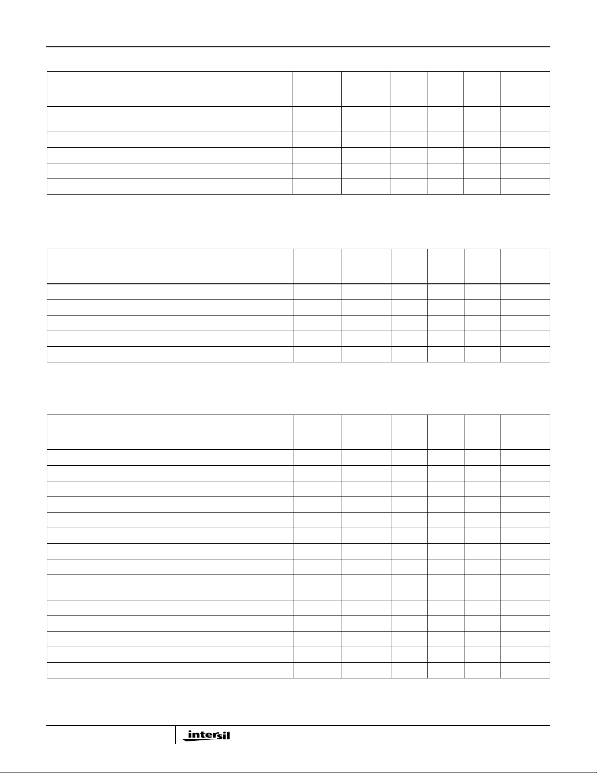
HFA3761
AC Electrical Specifications, I/Q Down Converter Individual Performance V
(NOTE 11)
TEST
PARAMETER
Demodulator Differential Output Level at 4K Load,
(Output Controlled By AGC Action)
Demodulator Amplitude Balance A 25 -1.0 - 1.0 dB
Demodulator Phase Balance at 286MHz A 25 -4 - 4 Degrees
Demodulator Phase Balance at 400MHz B 25 -4 - 4 Degrees
Demodulator Output 1dB Compression Voltage at 4K Load B 25 - 1.25 - V
NOTE:
11. A = Production Tested, B = Based on Characterization, C = By Design.
AC Electrical Specifications, LO Individual Performance V
PARAMETER
2XLO Input Frequency Range (2 X Input Range) B 25 20 - 800 MHz
2XLO Input Current Range C 25 50 200 300 µA
2XLO Input Impedance C 25 - 130 - Ω
Buffered LO Output Voltage, Single Ended C 25 50 100 - mV
Buffered LO Output Impedance C 25 - 50 - Ω
NOTE:
12. A = Production Tested, B = Based on Characterization, C = By Design.
LEVEL TEMP. (oC) MIN TYP MAX UNITS
B 25 400 500 560 mV
= 4.5V to 5.5V
CC
(NOTE 12)
TEST
LEVEL TEMP. (oC) MIN TYP MAX UNITS
= 4.5V to 5.5V (Continued)
CC
P-P
P-P
RMS
P-P
AC Electrical Specifications, RX 5TH Order LPF Individual Performance V
(NOTE 13)
TEST
PARAMETER
RX LPF 3dB Bandwidth, Sel0 = 0, Sel1 = 0 A 25 1.8 2.20 2.4 MHz
RX LPF 3dB Bandwidth, Sel0 = 1, Sel1 = 0 A 25 3.6 4.40 4.8 MHz
RX LPF 3dB Bandwidth, Sel0 = 0, Sel1 = 1 A 25 7.4 8.80 9.6 MHz
RX LPF 3dB Bandwidth, Sel0 = 1, Sel1 = 1 A 25 14.8 17.60 19.2 MHz
RX LPF Sel0, Sel1 Tuning Speed B 25 - - 1 µs
RX LPF 3dB Bandwidth Tuning A 25 -20 - +20 %
LPF Tune Nominal Resistance B 25 - 787 - Ω
RX LPF Voltage Gain A 25 -1.0 0 1.0 dB
RX LPF Single Ended Output Voltage Swing at 2kΩ Load
(Controlled By AGC Action)
RX LPF Differential Input Impedance A 25 4 5 - kΩ
RX I/Q Channel Amplitude Match A Full -1 - 1 dB
RX I/Q Channel Phase Match A Full -4 - 4 Degrees
RX LPF Total Harmonic Distortion B 25 - 3 6 %
LPF Output Impedance, Single-Ended C 25 - 50 - Ω
NOTE:
13. A = Production Tested, B = Based on Characterization, C = By Design.
LEVEL TEMP. (oC) MIN TYP MAX UNITS
B 25 - - 550 mV
= 4.5V to 5.5V
CC
P-P
4-8

HFA3761
TABLE 1. LOW PASS FILTER PROGRAMING AND TUNING INFORMATION
f
MODE LPF SEL1 LPF SEL0
BW0 0 0 2.2MHz
BW1 0 1 4.4MHz
BW2 1 0 8.8MHz
BW3 1 1 17.6MHz
3dB
(NOMINAL R
TUNE
)
f
3dBNOMINAL
--------------------------------------------------- -=
-10 -5 0 +5 +10 +15
[(787 - R
TUNE
+20%
-20%
PERCENT OF NOMINAL FREQUENCY
-30
-25 -20 -15
f
TUNED
3dB
FREQUENCY R
20% Low 984Ω
Nominal 787Ω
20% High 656Ω
FIGURE 1. TYPICAL f
R
)/R
3dB
TUNE
TUNE
vs R
∗
787
]* 100%
TUNE
TUNE
+20
+25
+30
4-9
 Loading...