

TM
HFA3683A
Data Sheet June 2000
2.4GHz RF/IF Converter and Synthesizer
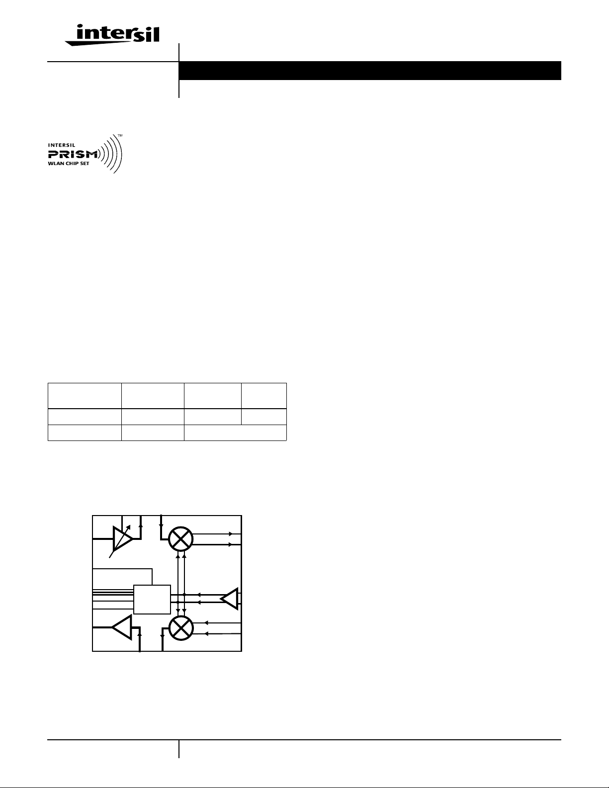
The HFA3683A is a monolithic SiGe
half-duplex RF/IF transceiver designed
to operate in the 2.4GHz ISM band.
The receive chain featuresalownoise,
gain selectableamplifier (LNA) followed
by a down-converter mixer. An up-converter mixer and a
high performance preamplifier compose the transmit chain.
The remaining circuitry comprises a high frequency Phase
Locked Loop (PLL) synthesizer with a three wire
programmable interface for local oscillator applications.
A reduced filter count is realized by multiplexing the receive
and transmit IF paths and by sharing a common differential
matching network. Furthermore, both transmit and receive
RF amplifiers can be directly connected to mixers. The
inherent image rejection of both the transmit and receive
functions allow this economic advantage.
The HFA3683A is housed in a 64 lead TQFP package well
suited for PCMCIA board applications.
File Number 4634.5
Features
• Highly Integrated
• Multiplexed RX/TX IF Path Utilizes Single IF Filter
• Programmable Synthesizer
• Gain Selectable LNA
• Power Management/Standby Mode
• Single Supply 2.7V to 3.3V Operation
Cascaded LNA/Mixer (High Gain)
• Gain . . . . . . . . . . . . . . . . . . . . . . . . . . . . . . . . . . . . . .25dB
• SSB Noise Figure. . . . . . . . . . . . . . . . . . . . . . . . . . . 3.7dB
• Input IP3. . . . . . . . . . . . . . . . . . . . . . . . . . . . . . . . -13dBm
• IF Frequency . . . . . . . . . . . . . . . . . . . 280MHz to 600MHz
Cascaded LNA/Mixer (Low Gain)
• Gain . . . . . . . . . . . . . . . . . . . . . . . . . . . . . . . . . . . . . .-5dB
• Input P1dB . . . . . . . . . . . . . . . . . . . . . . . . . . . . . +2.5dBm
Ordering Information
PART
NUMBER
HFA3683AIN -40 to 85 64 Ld TQFP Q64.10x10
HFA3683AIN96 -40 to 85 Tape and Reel
TEMP. RANGE
(oC) PACKAGE PKG. NO.
Simplified Block Diagram
RX_MX_IN
RF_OUT
H/L
RX_IN
CP_DO
INTERFACE
REF_IN
TXA_OUT
PLL
MODULE
RX_MX_OUT
LO_IN
TX_MX_IN
• IF Frequency . . . . . . . . . . . . . . . . . . . 280MHz to 600MHz
Cascaded Mixer/Preamplifier
• Transmit Cascaded Mixer/Preamplifier Gain . . . . . . .25dB
• SSB Noise Figure. . . . . . . . . . . . . . . . . . . . . . . . . . . .10dB
• Output P1dB. . . . . . . . . . . . . . . . . . . . . . . . . . . . . . . 4dBm
• IF Frequency . . . . . . . . . . . . . . . . . . . 280MHz to 600MHz
Applications
• IEEE802.11 1MBPS and 2MBPS Standard
• Systems Targeting IEEE802.11, 11MBPS Standard
• Wireless Local Area Networks
• PCMCIA Wireless Transceivers
• ISM Systems
• TDMA Packet Protocol Radios
TXA_IN
2-1
TX_MX_OUT
1-888-INTERSIL or 321-724-7143 | Intersil and Design is a trademark of Intersil Corporation. | Copyright © Intersil Corporation 2000
CAUTION: These devices are sensitive to electrostatic discharge; follow proper IC Handling Procedures.
PRISM® is a registered trademark of Intersil Corporation. PRISM logo is a trademark of Intersil Corporation.
Pinout
HFA3683A
HFA3683A
(TQFP)
TOP VIEW
PTAT_RES
ITAT_RES1
REF_IN
PRE_VCC1
GND
GND
GND
SYN_VCC2
GND
RX_MX_IN
CP_D0
CP_VCC2
GND
TX_MX_IN+
48
47
46
45
44
43
42
41
40
39
38
37
36
35
34
33
LD
GND
RX_MX_OUT+
RX_MX_OUTTX_MX_INGND
RX_LO_DRIVER_VCC1
GND
LO_VCC1
GND
LO_INLO_IN+
GND
TX_LO_DRIVER_VCC1
TX_MX_VCC1
TX_MX_VCC1
TX_MX_VCC1
TX_MX_OUT
TX_MX_VCC1
GND
LNA_VCC1
GND
RX_IN
GND
BIAS1_VCC1
GND
H/L
PE2
PE1
TX_VCC1
GND
TXA_OUT
GND
GND
GND
GND
COL_OUT
GND
RF_OUT
GND
ITAT_RES2
BIAS2_VCC1
6463 62 61 60 59 58 57 56 55 54 53 52 51 50 49
1
2
3
4
5
6
7
8
9
10
11
12
13
14
15
16
17 18 19 20 21 22 23 24 25 26 27 28 29 30 31 32
LE
GND
CLK
DAT A
REF_BY
GND
TXA_IN
TX_VCC1
Pin Description
PIN NAME DESCRIPTION
2 LNA_VCC1 Low Noise Amplifier Positive Power Supply.
4 RX_IN LowNoise Amplifier RF Input, internally DC coupled and requires an external blocking capacitor. A shunt capacitor to
ground matches the input for return loss and optimum NF.
6 BIAS1_VCC1 Bias Positive Power Supply for the LNA and Preamplifier.
8 H/L High or Low Gain Select, controls the LNA high and low gain modes.
9 PE2 This pin alongwith pinPE1 and bitM(0) ofPLL_PE determine which of variousoperational modes willbe active. Please
refer to the Power Enable Truth Table.
10 PE1 This pin alongwith pinPE2 and bitM(0) ofPLL_PE determine which of variousoperational modes willbe active. Please
refer to the Power Enable Truth Table.
11 TX_VCC1 Transmit Amplifier Positive Power Supply, requires a high quality decoupling capacitor and a short return path.
13 TXA_OUT Transmit Amplifier Output, internally matched to 50Ω, requires an external DC blocking capacitor.
17 TX_VCC1 Transmit Amplifier Positive Power Supply.
19 TXA_IN Transmit Amplifier Input, internally AC coupled.
21 LE Synthesizer Latch Enable, the serial interface is active when LE is low and the serial data is latched into defined
registers on the rising edge of LE.
22 DATA Synthesizer Serial Data Input, clocked in on the rising edge of the serial clock, MSB first.
23 CLK Synthesizer Clock, DATA is clocked in on the rising edge of the serial clock, MSB first.
24 REF_BY Synthesizer Reference Frequency Input Bypass, internally DC coupled and requires an external bypass to ground
when REF_INis used as a Single Ended input, alternatively,requires an external AC coupling capacitor when usedas
a differential input.
25 REF_IN Synthesizer Reference Frequency Input, internally DC coupled and requires an external AC coupling capacitor.
2-2

HFA3683A
Pin Description (Continued)
PIN NAME DESCRIPTION
27 SYN_VCC2 Synthesizer Positive Power Supply.
29 CP_VCC2 Synthesizer Charge Pump Positive Power Supply.
30 CP_DO Synthesizer Charge Pump Output, feeds the PLL loop filter.
32 LD Synthesizer Lock Detect Output.
33 TX_MX_VCC1 Transmit Mixer Positive Power Supply.
34 TX_MX_OUT Transmit Mixer RF output, internal AC coupled and internally matched to 50Ω.
35 TX_MX_VCC1 Transmit Mixer Positive Power Supply.
36 TX_MX_VCC1 Transmit Mixer Positive Power Supply.
37 TX_MX_VCC1 Transmit Mixer Positive Power Supply.
38 TX_LO_Driver_
VCC1
40 LO_IN+ Local Oscillator Positive Input, internally AC coupled, internally matched to 50Ω when the LO is driven single ended
41 LO_IN- Local Oscillator NegativeInput,internally ACcoupled, differential orsingle ended capability,ground externally forsingle
43 LO_VCC1 LO Buffer Positive Power Supply.
45 RX_LO_DRIVER
_VCC1
47 TX_MX_IN- Transmit Mixer NegativeInput, internallyDC coupled,high impedanceinput. Designedto sharea commonIF matching
48 RX_MX_OUT- Receive Mixer Negative Output, open collector, high impedance output. Designed to share a common IF matching
49 RX_MX_OUT+ Receive Mixer Positive Output, open collector, high impedance output. Designed to share a common IF matching
50 TX_MX_IN+ Transmit Mixer PositiveInput, internally DC coupled, high impedance input. Designed to share a common IF matching
52 RX_MX_IN Receive Mixer RF Input, internally DC coupled and requires external AC coupling as well as RF matching. The
54 PRE_VCC1 PLL Prescaler Positive Power Supply.
56 ITAT_RES1 Connection toexternalresistor setsthe receive andtransmitmixers tail currents,independent of AbsoluteTemperature.
57 PTAT_RES Connection to external resistorsets thereceive and transmitmixers tail currents, proportionalto Absolute Temperature.
58 BIAS2_VCC1 Bias Positive Power Supply for the receive and transmit mixers.
59 ITAT_RES2 Connection to external resistor sets the LNA and Preamplifier bias currents, independent of Absolute Temperature.
61 RF_OUT Low Noise Amplifier RF Output, internally AC coupled and internally matched to 50Ω.
63 COL_OUT LNA Collector Output,requires abypasscapacitance which isresonant with thePC boardparasitics.A small resistance
All
Others
GND Circuit Ground Pins (Quantity 23 each).
Transmit LO Driver Positive Power Supply.
and the LO_IN- is grounded.
ended operation.
Receiver LO Driver Positive Power Supply.
network/IF SAW filter with the receive mixer. Care should be exercised regarding the PC board layout to avoid
interference and noise pickup. Layout symmetry andmanagement of PC board parasiticsis also criticalfor maximizing
the bandwidth of the IF matching network.
network/IF SAW filter with the transmit mixer. Care should be exercised regarding the PC board layout to avoid
interference and noise pickup. Layout symmetry andmanagement of PC board parasiticsis also criticalfor maximizing
the bandwidth of the IF matching network.
network/IF SAW filter with the transmit mixer. Care should be exercised regarding the PC board layout to avoid
interference and noise pickup. Layout symmetry andmanagement of PC board parasiticsis also criticalfor maximizing
the bandwidth of the IF matching network.
network/IF SAW filter with the receive mixer. Care should be exercised regarding the PC board layout to avoid
interference and noise pickup. Layout symmetry andmanagement of PC board parasiticsis also criticalfor maximizing
the bandwidth of the IF matching network.
recommend network consists of a 3.3pF series capacitor followed by a small series inductance of 1.4nH and then a
1.2nH shunt inductor. The series inductance is best implemented on the PC board using a narrow transmission line
inductor.
(20Ω) in series with the main PC board VCC buss is recommended to provide isolation from other VCC bypass
capacitors. This ensures the image rejection performance of the LNA is maintained.
2-3
HFA3683A
Absolute Maximum Ratings Thermal Information
Supply Voltage. . . . . . . . . . . . . . . . . . . . . . . . . . . . . . . . . . . . . . 3.6V
Voltage on Any Other Pin. . . . . . . . . . . . . . . . . . . -0.3 to VCC+0.3V
VCC to VCC Decouple . . . . . . . . . . . . . . . . . . . . . . . . . -0.3 to +0.3V
Any GND to GND. . . . . . . . . . . . . . . . . . . . . . . . . . . . . -0.3 to +0.3V
Pins 4, 19, 52, 56, 57 and 59. . . . . . . . . . . . . . . . . . . . . 0.3 to +0.6V
Operating Conditions
Temperature Range. . . . . . . . . . . . . . . . . . . . . . . . . . . . -40 to 85oC
Supply Voltage Range. . . . . . . . . . . . . . . . . . . . . . . . . .2.7V to 3.3V
CAUTION: Stresses above those listed in “Absolute Maximum Ratings” may cause permanent damage to the device. This is a stress only rating and operation of the
device at these or any other conditions above those indicated in the operational sections of this specification is not implied.
NOTE:
1. θJA is measured with the component mounted on an evaluation PC board in free air.
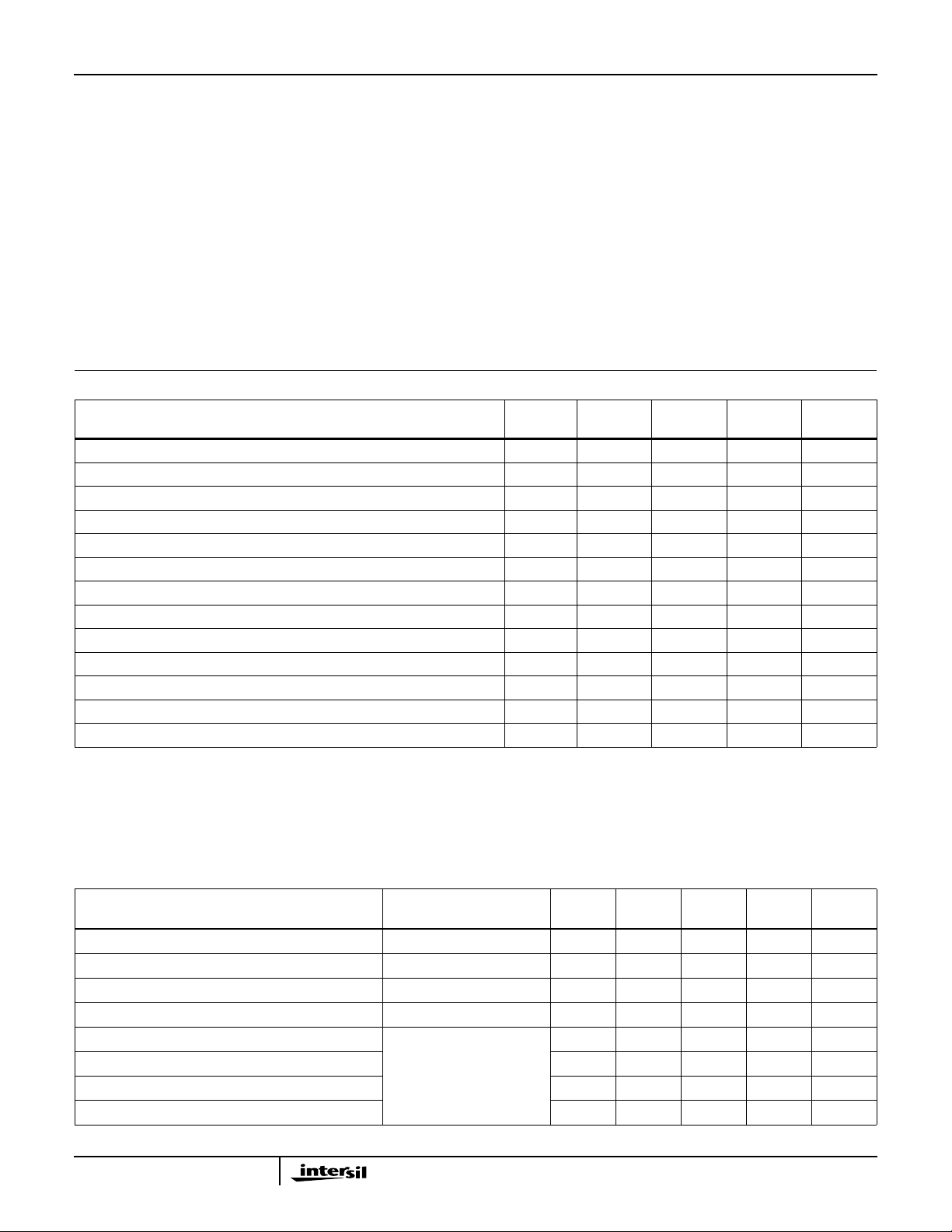
General Electrical Specifications
PARAMETER
Supply Voltage Full 2.7 - 3.3 V
Receive Total Supply Current (LNA in High Gain) 25 - 33 38 mA
Receive Total Supply Current (LNA in Low Gain) 25 - 27 32 mA
Transmit Total Supply Current 25 - 40 45 mA
Standby Total Supply Current (PLL and LO Buffers Active) 25 - 6 8 mA
TX/RX Power Down Supply Current Full - 10 100 µA
TX/RX/Power Down Time (Note 2) Full - 1 10 µs
RX/TX, TX/RX Switching Time (Note 2) Full - 0.2 1 µs
CMOS Low Level Input Voltage (CLK, DATA, LE) (Note 3) Full - - 0.3V
CMOS High Level Input Voltage (CLK, DATA, LE) (Note 3) Full 0.7V
CMOS High or Low Level Input Current (CLK, DATA, LE) Full -3.0 - +3.0 µA
Control Logic Low Level Input Voltage (H/L, PE1, PE2) (Note 4) Full -0.3 - 0.5 V
Control Logic High Level Input Voltage (H/L, PE1, PE2) (Notes 3 and 4) Full V
NOTES:
2. TX/RX/TX switching time and power Down/Up time are dependent on external components.
is thesupply voltage of external Control sources.
3. V
DD
4. These three pins H/L, PE1 and PE2 are not connected to CMOS circuitry and have different thresholds from all other control pins.
Thermal Resistance (Typical, Note 1) θJA (oC/W)
TQFP Package. . . . . . . . . . . . . . . . . . . . . . . . . . . . . 65
Maximum Junction Temperature (Plastic Package). . . . . . . . .150oC
Maximum Storage Temperature Range. . . . . . . . . . -65oC to 150oC
Maximum Lead Temperature (Soldering 10s) . . . . . . . . . . . . .300oC
(TQFP - Lead Tips Only)
TEMP.
(oC) MIN TYP MAX UNITS
V
DD
DD-0.5
DD
- 3.6 V
--V
Cascaded LNA/Mixer AC Electrical Specifications Assumes a direct connection between the LNA and Mixer , IF = 374MHz,
LO = 2075MHz at -6dBm, VCC = 2.7 Unless Otherwise Specified
TEMP.
PARAMETER TEST CONDITIONS
RF Frequency Range Full 2400 - 2500 MHz
IF Frequency Range Full 280 374 600 MHz
LO Frequency Range Full 1800 - 2220 MHz
LO Input Drive Level Single End or Differential Full -10 -6 0 dBm
Power/Voltage Gain High Gain Mode Full 21.5 25 29 dB
Noise Figure SSB Full - 3.7 5.0 dB
Input IP3 Full -17.5 -11 - dBm
Input P1dB Full -27.5 -22 - dBm
2-4
(oC) MIN TYP MAX UNITS
HFA3683A
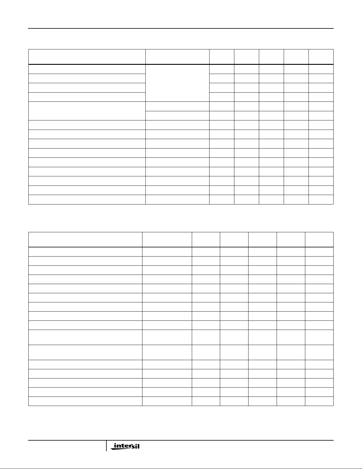
Cascaded LNA/Mixer AC Electrical Specifications Assumes a direct connection between the LNA and Mixer , IF = 374MHz,
LO = 2075MHz at -6dBm, VCC = 2.7 Unless Otherwise Specified (Continued)
TEMP.
PARAMETER TEST CONDITIONS
Power/Voltage Gain Low Gain Mode Full -9 -5 -1 dB
Noise Figure 25 - 25 - dB
Output IM3 at -4dBm Input Tones Full -42 -40.5 -40 dBc
Input P1dB Full -1 +2.5 - dBm
LNA Input 50Ω VSWR High Gain Mode 25 1.28 1.65:1 2.0:1 -
Low Gain Mode 25 1.1:1 1.3:1 2.0:1 LO 50Ω VSWR LO = Single End 25 1.4:1 1.4:1 2.0:1 Differential IF Output Load Shared with TX 25 - 200 - Ω
IF Output Capacitance (Single Ended) 25 - 1.2 - pF
IF Output Resistance (Single Ended) 25 - 5.5 - kΩ
LO to Mixer RF Feedthrough (Uncascaded) 25 - -50 -20 dBm
LO to LNA Input Feedthrough (Cascaded, no filter) 25 -69 -60 -50 dBm
Gain Switching Speed at Full Scale - High to Low ±1dB settling Full - 0.03 0.1 µs
Gain Switching Speed at Full Scale - Low to High ±1dB settling Full - 0.25 0.3 µs
Image Rejection With Matching Network 25 - 14 - dB
(oC) MIN TYP MAX UNITS
Cascaded Transmit Mixer AC Electrical Specifications Assumes a direct connection between the Mixer and Preamplifier,
F = 374MHz, LO = 2075MHz at -6dBm, VCC = 2.7 Unless Otherwise
Specified.
TEMP.
PARAMETER TEST CONDITIONS
RF Frequency Range Full 2400 - 2500 MHz
IF Frequency Range Full 280 374 600 MHz
LO Frequency Range Full 1800 - 2220 MHz
Power Conversion Gain 200Ω In, 50Ω Out Full 21 25 29 dB
SSB Noise Figure Full - 10 15 dB
Output IP3 Full +12 +14 +20 dBm
Output P1dB Full +2 +4 +9 dBm
LO Input Drive Level Same as RX Full -10 -6 0 dBm
LO to Transmit Mixer RF Feedthrough (Uncascaded) 25 - -37 -20 dBm
LO to Transmit Amp. Output Feedthrough
(Uncascaded)
LO to Transmit Amp. Output Feedthrough
(Cascaded, no filter)
Preamplifier Output 50Ω VSWR 25 - 2.3:1 3.0:1 LO 50Ω VSWR LO = Single End 25 - 1.4:1 2.0:1 Differential IF Input Load Shared with RX 25 - 200 - Ω
IF Input Capacitance (Single Ended) 25 - 1.1 - pF
IF Input Resistance (Single Ended) 25 - 0.7 - kΩ
o
(
C) MIN TYP MAX UNITS
25 - -45 -30 dBm
25 - -15 -5 dBm
2-5

HFA3683A
Phase Lock Loop Electrical Specifications (See Notes 5 through 13)
TEMP.
o
PARAMETER TEST CONDITIONS
Operating LO Frequency (32/33 Prescaler) Full 1800 - 2220 MHz
Operating LO Frequency (64/65 Prescaler) Full 1800 - 3500 MHz
Reference Oscillator Frequency Full - - 50 MHz
Selectable Prescaler Ratios (P) Full 32/33 - 64/65 Swallow Counter Divide Ratio (A Counter) Full 0 - 127 Programmable Counter Divide Ratio (B Counter) Full 3 - 2047 Reference Counter Divide Ratio (R Counter) Full 3 - 32767 Reference Oscillator Sensitivity,Single orDifferential
Sine Inputs
Reference Oscillator Sensitivity, CMOS Inputs,
Single Ended or Complimentary
Reference Oscillator Duty Cycle CMOS Inputs 25 40 - 60 %
Charge Pump Sink/Source Current/Tolerance 250µA Selection ±25% 25 0.18 0.25 0.32 mA
Charge Pump Sink/Source Current/Tolerance 500µA Selection ±25% 25 0.375 0.50 0.625 mA
Charge Pump Sink/Source Current/Tolerance 750µA Selection ±25% 25 0.56 0.75 0.94 mA
Charge Pump Sink/Source Current/Tolerance 1mA Selection ±25% 25 0.75 1.0 1.25 mA
Charge Pump Sink/Source Mismatch Full - - 15 %
Charge Pump Output Compliance Full 0.5 - V
Charge Pump Supply Voltage Full 2.7 - 3.6 V
Serial Interface Clock Width High Level t
Low Level t
Serial Interface Data/Clk Set-Up Time t
Serial Interface Data/Clk Hold Time t
Serial Interface Clk/LE Set-Up Time t
Serial Interface LE Pulse Width t
CS
CH
ES
EW
CWH
CWL
NOTES:
5. The Serial data is clocked on the Rising Edge of the serial clock, MSB first. The serial Interface is active when LE is LOW. The serial Data is
latched into defined registers on the rising edge of LE.
6. As longas poweris applied,all registersettings willremain stored,including the power down state. The system may then come in and out of the
power down state without requiring the registers to be rewritten.
7. CMOS Reference Oscillator input levels are given in the General Electrical Specification section.
C) MIN TYP MAX UNITS
(
Full 0.5 - V
CC
V
PP
Full - CMOS - Note 7
-0.5 V
CC2
Full 20 - - ns
Full 20 - - ns
Full 20 - - ns
Full 10 - - ns
Full 20 - - ns
Full 20 - - ns
POWER ENABLE TRUTH TABLE
PLL_PE
PE1 PE2
(SERIAL BUS) STATUS
0 0 1 Power Down State, Registers in Save Mode, Inactive PLL, Active
Serial Interface
1 1 1 Receive State, Active PLL
1 0 1 Transmit State, Active PLL
0 1 1 Inactive Transmit and Receive States, Active PLL, Active Serial
Interface
X X 0 Inactive PLL, Disabled PLL Registers, Active Serial Interface
NOTE:
8. PLL_PE is controlledvia the serialinterface, and can be used to disable the synthesizer. The actual synthesizer control is a logic AND function
of PLL_PE andthe resultof thelogic ORfunction of PE1 and PE2.PE1 andPE2 directlycontrol the power enable functionality of theLO buffers.
2-6

HFA3683A
PLL Synthesizer Table
REGISTER
DEFINITION
SERIAL BITS
R Counter 0 0 R(0) R(1) R(2) R(3) R(4) R(5) R(6) R(7) R(8) R(9) R(10) R(11) R(12) R(13) R(14) X (Don’t Care)
A/B Counter 0 1 A(0) A(1) A(2) A(3) A(4) A(5) A(6) B(0) B(1) B(2) B(3) B(4) B(5) B(6) B(7) B(8) B(9) B(10)
Operational
Mode
Reference Frequency Counter/Divider
BIT DESCRIPTION
R(0-14) Least significant bitR(0) to mostsignificant bit R(14) of the divide by R counter. The Reference signal frequency is divided down
LO Frequency Counters/Dividers
BIT DESCRIPTION
A(0-6) Least significant bit A(0) to most significant bit A(6) of a 7-bit Swallow counter and LSB B(0) to MSB B(10) of the 11-bit divider.
B(0-11)
LSB 1 2 345678910111213141516171819MSB
1 0 M(0) 0 M(2) M(3) M(4) M(5) M(6) M(7) M(8) 0 0 0 0 M(13) M(14) M(15) X X
by this counter and is compared with a divided LO by a phase detector.
The LO frequency is divided down by [P*B+A], where P is the Prescaler divider set by bit M(2). This divided signal frequency is
compared by a phase detector with the divided Reference signal.
Operational Modes
BIT DESCRIPTION
M(0) (PLL_PE), Phase Lock Loop Power Enable. 1 = Enable, 0 = Power Down. Serial port always on.
M(2) Prescaler Select. 0 = 32/33, 1 = 64/65
M(3)
M(4)
M(5)
M(6)
M(7)
M(8)
M(13)
M(14)
M(15)
Charge Pump Current Setting M(4) M(3) OUTPUT SINK/SOURCE
0 0 0.25mA
0 1 0.50mA
1 0 0.75mA
1 1 1.00mA
Charge Pump Sign M(6) M(5)
0 0 Source Current if LO/ [P*B+A] < Ref/R
0 1 Source Current if LO/ [P*B+A] > Ref/R
LD Pin Multiplex Operation M(13) M(8) M(7) OUTPUT AT PIN LD
0 0 X Lock Detect Operation
0 1 X Short to GND
1 0 X Serial Register Read Back
1 1 0 Ref. Divided by R Waveform
1 1 1 LO Divided by [P*B+A]
Charge Pump Operation/Test M(15) M(14) OPERATION/TEST
0 0 Normal Operation
0 1 Charge Pump Constant Current Source
1 0 Charge Pump Constant Current Sink
1 1 High Impedance State
Waveform
2-7
HFA3683A
DAT A
REF_IN
BIT 20: MSB
R COUNTER
R
TO
DC OFFSET
CAL
BIT 19
V
ISOURCE
CP_D0
ISINK
RESET
N COUNTER
A
RESET
DUAL MODULUS
B
VCONTROL
FIGURE 1. PLL SIMPLIFIED BLOCK DIAGRAM
BIT 10 BIT 9 BIT 1 BIT 1: LSB
CONTROL
P/P+1
PRESCALER
TO LO DIVIDE BY 2 DRIVERS
LO_IN+
VCO
CLOCK
LE
OR
LE
t
CS
t
CH
NOTES:
9. Parenthesis data indicates programmable reference divider data.
10. Data shifted into register on clock rising edge.
11. Data is shifted in MSB first.
FIGURE 2. SERIAL DATA INPUT TIMING
t
t
CWH
CWL
t
EW
t
ES
2-8

LD
HFA3683A
f
R
f
P
D
O
fR > f
H
P
fR = f
P
Z
III
L
fR < f
P
fR < f
P
fR < f
NOTES:
12. Phase difference detection range: -2π to +2π.
13. The minimum width pump up and pump down current pulses occur at the DO pin when the loop is locked.
FIGURE 3. PHASE COMPARATOR AND INTERNAL CHARGE PUMP CHARACTERISTICS
P
2-9

HFA3683A
Typical Evaluation Board Application
C12
0.01µF
0.01µF
R11
LNA_OUT
VCC1
LNA_IN
C5
R3
100K
LNA_H/L
R4
100K
PE2
PE1
R5
100K
PRE_OUT
GP4
(NO FIT)
C1
0.5pF
GP1
R6
GP2
GP3
C9
XTAL__VCC
(NO FIT)
R16
0.01µF
100K
7pF
C53
0
R2 20
C14
C8
C29
100pF
PRE_IN
C54
4.7µF
7pF
VCC1
0.01µF
0.1µF
R1
C3
C2
C4
C26
1.2pF
C33
3.9pF
7.0pF
7.0pF
0
C10
.01µF
7pF
4
VDD
1
ENB
2
GND
11.5K
GND
1
LNA_VCC1
2
GND
3
RX_IN
4
GND
5
BIAS1_VCC1
6
GND
7
H/L
8
PE2
9
PE1
10
TX_VCC1
11
GND
12
TXA_OUT
13
GND
14
GND
15
16
GND
C36
0.01µF
U6
OUT
F4106
VCC1
C7
0.01µF
GND
GND
COL_OUT
TX_VCC1
GND
TXA_IN
C19
R10
3
1.5K
0.56µH
RF_OUT
GND
L1
GND
ITAT_RES2
BIAS2_VCC1
HFA3683AIN
DAT ALECLK
1000pF
C32
1000pF
C6
22pF
C17
R12 1.5K
R13
9.53K
C16
0.01µF
GND
GND
PTAT_RES
ITAT_RES1
PRE_VCC1
RX_LO_DRIVER_VCC1
U1
TX_LO_DRIVER_VCC1
REF_BY
REF_IN
GND
SYN_VCC2
GND
100pF
C20
C21
R8
0
(NO FIT)
REF_IN
(NO FIT)
L23
3.3pF
49505152535455565758596061626364
GND
RX_MX_IN
TX_MX_IN+
RX_MX_OUT-
TX_MX_IN-
GND
GND
LO_VCC1
GND
LO_IN-
LO_IN+
GND
TX_MX_VCC1
TX_MX_VCC1
TX_MX_VCC1
TX_MX_OUT
TX_MX_VCC1
GND
CP_VCC2
CP_D0
29
323130282726252423222120191817
(NO FIT)
C22
47pF
0.1µF
R27
10K
1.2nH
RX_MX_OUT+
48
47
46
45
44
43
42
41
40
39
38
37
36
35
34
33
C39
0.01µF
LD
C23
LD
R25
20K
R28
10K
DAT A
CLK
C40
47pF
R26
R29
10K
C25
L10
39nH
L9
39nH
0.01µF
LE
GND
RX_MIX_IN
220pF
R15
1.1K
R14
1.1K
VCC1
C38
0.01µF
R30
20K
VCC2
20K
N/C
UP2
UP1
2-10
N/C

HFA3683A
Typical Evaluation Board Application (Continued)
C27
R36
3.3pF
0
T1
IF_IN/OUT
C31
3.3pF
220pF
C37
TX_MIX_OUT
R9
4
C46
0.1µF
C51
0.1µF
+
4.7µF
C47
C63
+
4.7µF
(NO FIT)
0
C34
0.01µF
C52
VCC2
U4
OUT IN
MAX8867
2
C58
1000pF
2
3
10pF
SHDN
BPGND
VCC
VCONT
3
1
5
10pF
ENFVZ5F81
GROUND
5A 5B 5C 5D4
C49
C50
0.01µF
C55
RF
0.1µF
235
4
U2
1
C48
U3
6
R34
+
4.7µF
UPC2745TB
1
C56
R33
91
R35
10pF
82
82
D1
VCC_IN
GP5
VCC2
EXT_VCO
R17
R19
560
56
2-11
C62
C43
2700pF
VCC2
4.7µF
C61
C44
R21
R20
0.027µF
1.74K
0.1µF
3.48K
C45
4
300pF
OUT IN
MAX8867
SHDN
GND
2
BP
FILTER VALUES
BW 1KHz 10kHz
C43 0.068µF 2700pF
C44 0.68µF 0.027µF
R20 1.5K 3.48K
R21 649 1.74K
C45 0.01µF 330pF
U5
3
C60
1
5
C57
0.01µF
0.1µF
C59
(10KHz
DEFAUL T)
+
4.7µF

Typical Performance Curves
VCC = 3.30V
RF = 2.0GHz TO 3.0GHz
ROOM TEMP
Pin = -30.dBm
1
HFA3683A
SCALE
1dB/DIV
2
3
1
VCC = 3.30V
RF = 2.0GHz TO 3.0GHz
ROOM TEMP
Pin = -30.dBm
2
3
Marker 1 = 2.0GHz, Real = 17.6Ω, Imaginary = 35.2Ω
Marker 2 = 2.45GHz, Real = 18.2Ω, Imaginary = 60.1Ω
Marker 3 = 3.0GHz, Real = 24.6Ω, Imaginary = 82.5Ω
FIGURE 4. S11 LNA in HIGH GAIN
SCALE
5dB/DIV
2
VCC = 3.30V
RF = 2.0GHz TO 3.0GHz
1
ROOM TEMP
Pin = -30.dBm
Marker 1 = 2.0GHz, 14.9dB
Marker 2 = 2.45GHz, 13.4dB
Marker 3 = 3.0GHz, 9.1dB
FIGURE 5. S21 LNA in HIGH GAIN
VCC = 3.30V
RF = 2.0GHz TO 3.0GHz
ROOM TEMP
Pin = -30.dBm
3
1
3
2
Marker 1 = 2.0GHz, -50.3dB
Marker 2 = 2.45GHz, 36.9dB
Marker 3 = 3.0GHz, -32.8dB
FIGURE 6. S12 LNA in HIGH GAIN
Marker 1 = 2.0GHz, Real = 25.6Ω, Imaginary = 8.1Ω
Marker 2 = 2.45GHz, Real = 79.5Ω, Imaginary = -30.6Ω
Marker 3 = 3.0GHz, Real = 17.4Ω, Imaginary = -3.2Ω
FIGURE 7. S22 LNA in HIGH GAIN
2-12
Typical Performance Curves (Continued)
VCC = 3.30V
RF = 2.0GHz TO 3.0GHz
ROOM TEMP
Pin = -30.dBm
1
3
2
HFA3683A
SCALE
2dB/DIV
Marker 1 = 2.0GHz, Real = 21.5Ω, Imaginary = 42.5Ω
Marker 2 = 2.45GHz, Real = 20.4Ω, Imaginary = 64.0Ω
Marker 3 = 3.0GHz, Real = 22.6Ω, Imaginary = 87.0Ω
FIGURE 8. S11 LOW GAIN LNA
SCALE
5dB/DIV
1
2
1
2
VCC = 3.30V
RF = 2.0GHz TO 3.0GHz
ROOM TEMP
Pin = -30.dBm
3
Marker 1 = 2.0GHz, -16.4dB
Marker 2 = 2.45GHz, -16.4dB
Marker 3 = 3.0GHz, -17.2dB
FIGURE 9. S21 LOW GAIN LNA
VCC = 3.30V
RF = 2.0GHz TO 3.0GHz
ROOM TEMP
Pin = -30.dBm
3
3
1
2
VCC = 3.30V
RF = 2.0GHz TO 3.0GHz
ROOM TEMP
Pin = -30.dBm
Marker 1 = 2.0GHz, -16.4dB
Marker 2 = 2.45GHz, 16.5dB
Marker 3 = 3.0GHz, -17.6dB
FIGURE 10. S12 LOW GAIN LNA
Marker 1 = 2.0GHz, Real = 29.4Ω, Imaginary = 16.5Ω
Marker 2 = 2.45GHz, Real = 77.7Ω, Imaginary = 22.9Ω
Marker 3 = 3.0, Real = 43.0Ω, Imaginary = 21.7Ω
FIGURE 11. S22 LOW GAIN LNA
2-13

Typical Performance Curves (Continued)
HFA3683A
VCC = 3.30V
RF = 2.0GHz TO 3.0GHz
ROOM TEMP
Pin = -30dBm
3
2
1
Marker 1 = 2.0GHz, Real = 17.4Ω, Imaginary = -14.8Ω
Marker 2 = 4.5GHz, Real = 14.1Ω, Imaginary = 9.8Ω
Marker 3 = 3GHz, Real = 13.1Ω, Imaginary = 33.8Ω
FIGURE 12. S11 RX MIXER
VCC = 3.30V
RF = 2.0GHz TO 3.0GHz
ROOM TEMP
Pin = -30dBm
2
VCC = 3.30V
RF = 2.0GHz TO 3.0GHz
ROOM TEMP
Pin = -30.dBm
2
3
1
Marker 1 = 2.0GHz, Real = 23.4Ω, Imaginary = 5.9Ω
Marker 2 = 2.45GHz, Real = 59.9Ω, Imaginary = 55.7Ω
Marker 3 = 3.0GHz, Real = 72.4Ω, Imaginary = 12.5Ω
FIGURE 13. S22 TX MIXER
SCALE
1dB/DIV
1
3
Marker 1 = 2.0GHz, Real = 13.2Ω, Imaginary = 1.2Ω
Marker 2 = 2.45GHz, Real = 11.2Ω, Imaginary = 31.6Ω
Marker 3 = 3.0GHz, Real = 46.6Ω, Imaginary = 21.7Ω
FIGURE 14. S11 PREAMP
1
Marker 1 = 2.0GHz, 10.7dB
Marker 2 = 2.45GHz, 15.5dB
Marker 3 - 3.0GHz, 12.5dB
FIGURE 15. S21 PREAMP
2
3
VCC = 3.30V
RF = 2.0GHz TO 3.0GHz
ROOM TEMP
Pin = -30.dBm
2-14
Typical Performance Curves (Continued)
SCALE
5dB/DIV
HFA3683A
V
= 3.30V
CC
RF = 2.0GHz TO 3.0GHz
ROOM TEMP
Pin = -30.dBm
3
2
1
VCC = 3.30V
RF = 2.0GHz TO 3.0GHz
ROOM TEMP
Pin = -30.dBm
Marker 1 = 2.0GHz, -35.2dB
Marker 2 = 2.45GHz, 30.1dB
Marker 3 = 3.0GHz, -33.3dB
FIGURE 16. S12 PREAMP
GAIN 14.3dB AT 2.7V, 13.8dB AT 3.3V
NOISE FIGURE 3.5dB AT 2.7V, 3.9dB AT 3.3V
2.7V
3
1
2
Marker 1 = 2.0GHz, Real = 21.9Ω, Imaginary = 48.0Ω
Marker 2 = 2.45GHz, Real = 53.4Ω, Imaginary = 46.5Ω
Marker 3 = 3.0GHz, Real = 21.4Ω, Imaginary = 54.6Ω
FIGURE 17. S22 PREAMP
GAIN 16.5dB AT 2.7V, 15.7dB AT 3.3V
NOISE FIGURE 2.2dB AT 2.7V, 2.7dB AT 3.3V
2.7V
3.3V
TEMP = 125oC
GAIN 6dB/DIV
NF 3dB/DIV
3.3V
2.7V
2.4GHz 2.5GHz
FIGURE 18. LNA HIGH GAIN AND NOISE FIGURE vs SUPPLY
VOLTAGE
3.3V
TEMP = -40oC
GAIN 6dB/DIV
NF 3dB/DIV
3.3V
2.7V
2.4GHz 2.5GHz
FIGURE 19. LNA HIGH GAIN AND NOISE FIGURE vs SUPPLY
VOLTAGE
2-15

Typical Performance Curves (Continued)
HFA3683A
GAIN -16.7dB AT 2.7V, -15.0dB AT 3.3V
3.3V
2.7V
GAIN 6dB/DIV
2.4GHz
FIGURE 20. LNA LOW GAIN vs SUPPLY VOLTAGE FIGURE 21. LNA LOW GAIN vs SUPPLY VOLTAGE
GAIN AT CURSOR 7.5dB AT 2.7V, 7.6dB AT 3.3V
NOISE FIGURE AT CURSOR 8.7dB AT 2.7V, 8.4dB AT 3.3V
2.7V
GAIN 6dB/DIV
NF 3dB/DIV
2.7V
TEMP = 125oC
TEMP = 125oC
3.3V
2.5GHz
GAIN -13.3dB AT 2.7V, -12.7dB AT 3.3V
3.3V
2.7V
GAIN 6dB/DIV
2.4GHz 2.5GHz
GAIN AT CURSOR 9.5dB AT 2.7V, 9.6dB AT 3.3V
NOISE FIGURE AT CURSOR 7.0dB AT 2.7V, 6.9dB AT 3.3V
2.7V
2.7V
TEMP = -40oC
3.3V
TEMP = -40oC
RF 2.4GHz
IF 300MHz
FIGURE 22. RX MIXER GAIN AND SSB NOISE FIGURE vs
SUPPLY VOLTAGE
3.3V
RF 2.5GHz
IF 400MHz
GAIN 6dB/DIV
NF 3dB/DIV
RF 2.4GHz
IF 300MHz
3.3V
FIGURE 23. RX MIXER GAIN AND SSB NOISE FIGURE vs
SUPPLY VOLTAGE
RF 2.5GHz
IF 400MHz
2-16

HFA3683A
Thin Plastic Quad Flatpack Packages (TQFP)
E
E1
GAGE
PLANE
0o-7
D
D1
-D-
Q64.10x10 (JEDEC MS-026ACD ISSUE B)
64 LEAD THIN PLASTIC QUAD FLATPACK PACKAGE
INCHES MILLIMETERS
SYMBOL
NOTESMIN MAX MIN MAX
A - 0.047 - 1.20 -
A1 0.002 0.005 0.05 0.15 -
-A-
-B-
A2 0.038 0.041 0.95 1.05 -
b 0.007 0.010 0.17 0.27 6
b1 0.007 0.009 0.17 0.23 -
D 0.468 0.476 11.90 12.10 3
D1 0.390 0.397 9.9 10.10 4, 5
E 0.468 0.476 11.9 12.10 3
e
E1 0.390 0.397 9.9 10.10 4, 5
L 0.018 0.029 0.45 0.75 -
PIN 1
N64 647
e 0.020 BSC 0.50 BSC -
-H-
0.020
0.008
0o MIN
MIN
11o-13
A2
o
A1
0.08
0.003
0.09/0.16
0.004/0.006
SEATING
PLANE
A
-C-
D
A-B S
SCM
b
b1
0.08
0.003
NOTES:
1. Controlling dimension:MILLIMETER. Converted inch
dimensions are not necessarily exact.
2. All dimensions and tolerances per ANSI Y14.5M-1982.
3. Dimensions Dand E to be determinedat seatingplane .
4. Dimensions D1 andE1 to be determined at datum plane
-H-
.
5. Dimensions D1 and E1 do not include moldprotrusion.
Allowable protrusion is 0.25mm (0.010 inch) per side.
6. Dimension b does not includedambar protrusion. Allowable
dambar protrusion shall not cause the lead width to exceed
the maximum b dimension by more than 0.08mm (0.003
Rev. 0 7/98
-C-
inch).
BASE METAL
L
0.25
o
0.010
11o-13
o
WITH PLATING
0.09/0.20
0.004/0.008
7. “N” is the number of terminal positions.
All Intersil semiconductor products are manufactured, assembled and tested under ISO9000 quality systems certification.
Intersil semiconductor products are sold by descriptiononly.Intersil Corporation reserv esthe right to make changes in circuit design and/or specifications at any time without notice. Accordingly, the reader is cautioned to verify that data sheets are current before placing orders. Information furnished by Intersil is believed to be accurate and
reliable. However, no responsibility is assumed by Intersil or its subsidiaries for its use; nor for any infringements of patents or other rights of third parties which may result
from its use. No license is granted by implication or otherwise under any patent or patent rights of Intersil or its subsidiaries.
For information regarding Intersil Corporation and its products, see web site www.intersil.com
Sales Office Headquarters
NORTH AMERICA
Intersil Corporation
P. O. Box 883, Mail Stop 53-204
Melbourne, FL 32902
TEL: (321) 724-7000
FAX: (321) 724-7240
2-17
EUROPE
Intersil SA
Mercure Center
100, Rue de la Fusee
1130 Brussels, Belgium
TEL: (32) 2.724.2111
FAX: (32) 2.724.22.05
ASIA
Intersil (Taiwan) Ltd.
7F-6, No. 101 Fu Hsing North Road
Taipei, Taiwan
Republic of China
TEL: (886) 2 2716 9310
FAX: (886) 2 2715 3029
 Loading...