Intersil Corporation HFA3663 Datasheet

HFA3663
Data Sheet January 1999 File Number
2.3GHz UpConverter with Gain Control
™
The HFA3663 UpConverter with Gain
Control is a monolithic bipolar device
for up conversion applications in the
2.0GHz to 2.3GHz range.
Manufactured in the Intersil UHF1X
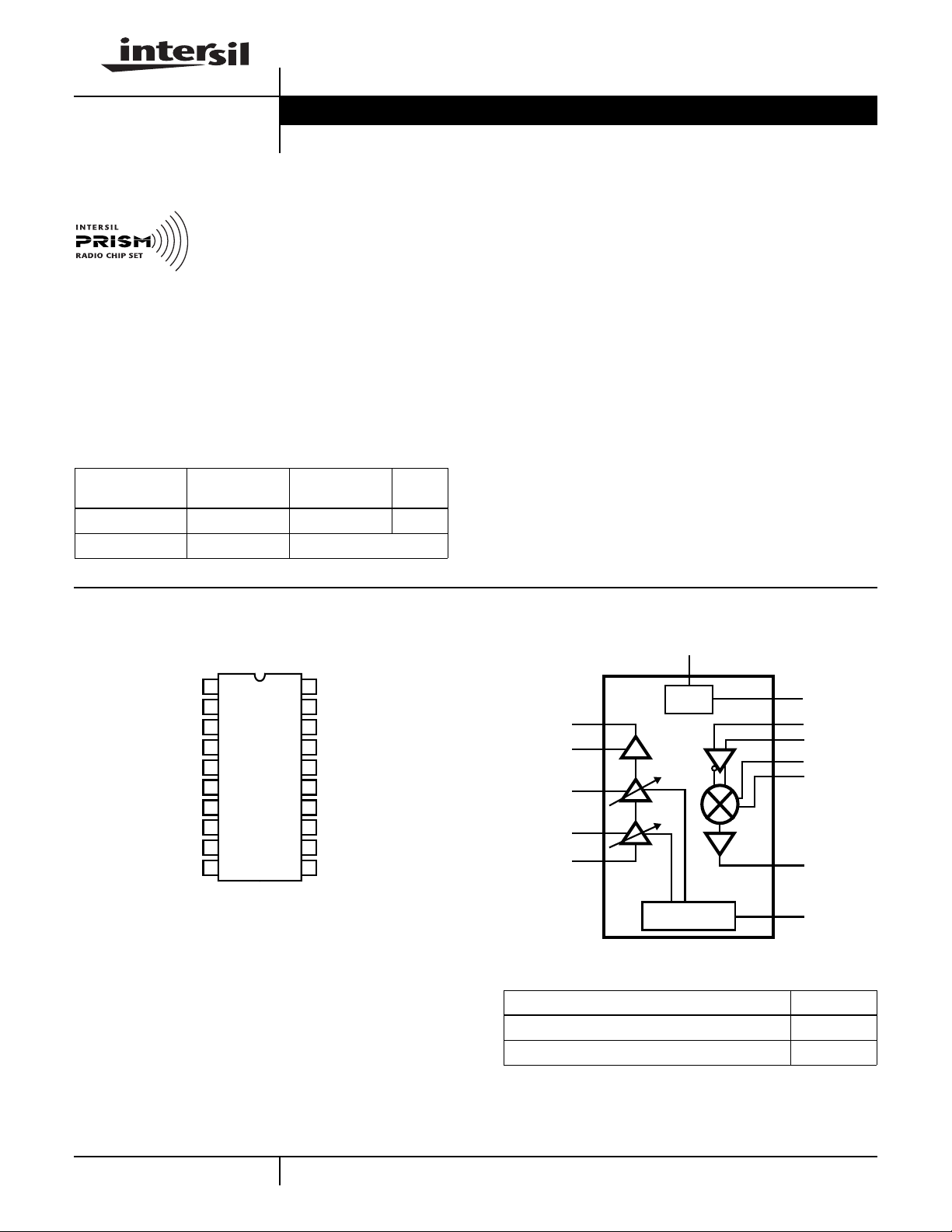
process, the device consists of a double balanced mixer
followedby a variablegain powerpreamp. An energy saving,
TTL Compatible, power enable input provides on/off bias
current control to the mixer and amplifier. The device
requires low drive levels from the local oscillator and is
housed in a small outline 20 lead SSOP package ideally
suited for PCMCIA card applications.
Ordering Information
TEMP.
PART NUMBER
RANGE (oC) PACKAGE
HFA3663IA -40 to 85 20 Ld SSOP M20.15
HFA3663IA96 -40 to 85 Tape and Reel
PKG.
NO.
4241.3
Features
• RF Frequency Range. . . . . . . . . . . . . . 2.0GHz to 2.3GHz
• IF Operation . . . . . . . . . . . . . . . . . . . . .10MHz to 400MHz
• Gain Control Range . . . . . . . . . . . . . . . . . . . . . . . . . .20dB
• Single Supply Operation. . . . . . . . . . . . . . . . .2.7V to 5.5V
• High Output 1dB Compression. . . . . . . . . . . . . . . . . 6dBm
• High Power Gain . . . . . . . . . . . . . . . . . . . . . . . . . . . .18dB
• Power Enable/Disable Control
Applications
• Wireless Local Loop Systems
• PCMCIA Wireless Transceiver
• Wireless Local Area Network Modems
• CDMA/TDMA Packet Protocol Radios
• Full Duplex Transceivers
• Portable Battery Powered Equipment
Pinout
PRE_VCC3
GND
PRE_OUT
GND
PRE_V
CC
GND
BIAS_V
CC
GND
PRE_IN
PRE_V
CC
2
1
1
2
3
4
5
6
7
8
9
10
HFA3663
TOP VIEW
TX_PE
20
LO_BY
19
LO_IN
18
GND
17
IF_IN
16
IF_BY
15
GND
14
TXM_RF
13
12
MIX_V
11
AGC_CTRL
CC
Block Diagram
BIAS_V
CC
BIAS
PRE_OUT
PRE_VCC3
PRE_V
PRE_V
CC
CC
PRE_IN
2
1
AGC CONTROL
POWER CONTROL TRUTH TABLE
STATE TX_PE
Power Down - Energy Saving Mode Low
Transmit Mode High
TX_PE
LO_BY
LO_IN
IF_IN
IF_BY
TXM_RF
AGC_CTRL
2-201
CAUTION: These devices are sensitive to electrostatic discharge; follow proper IC Handling Procedures.
http://www.intersil.com or 407-727-9207
PRISM® is a registered trademark of Intersil Corporation. PRISM logo is a trademark of Intersil Corporation.
| Copyright © Intersil Corporation 1999

Typical Application Diagram
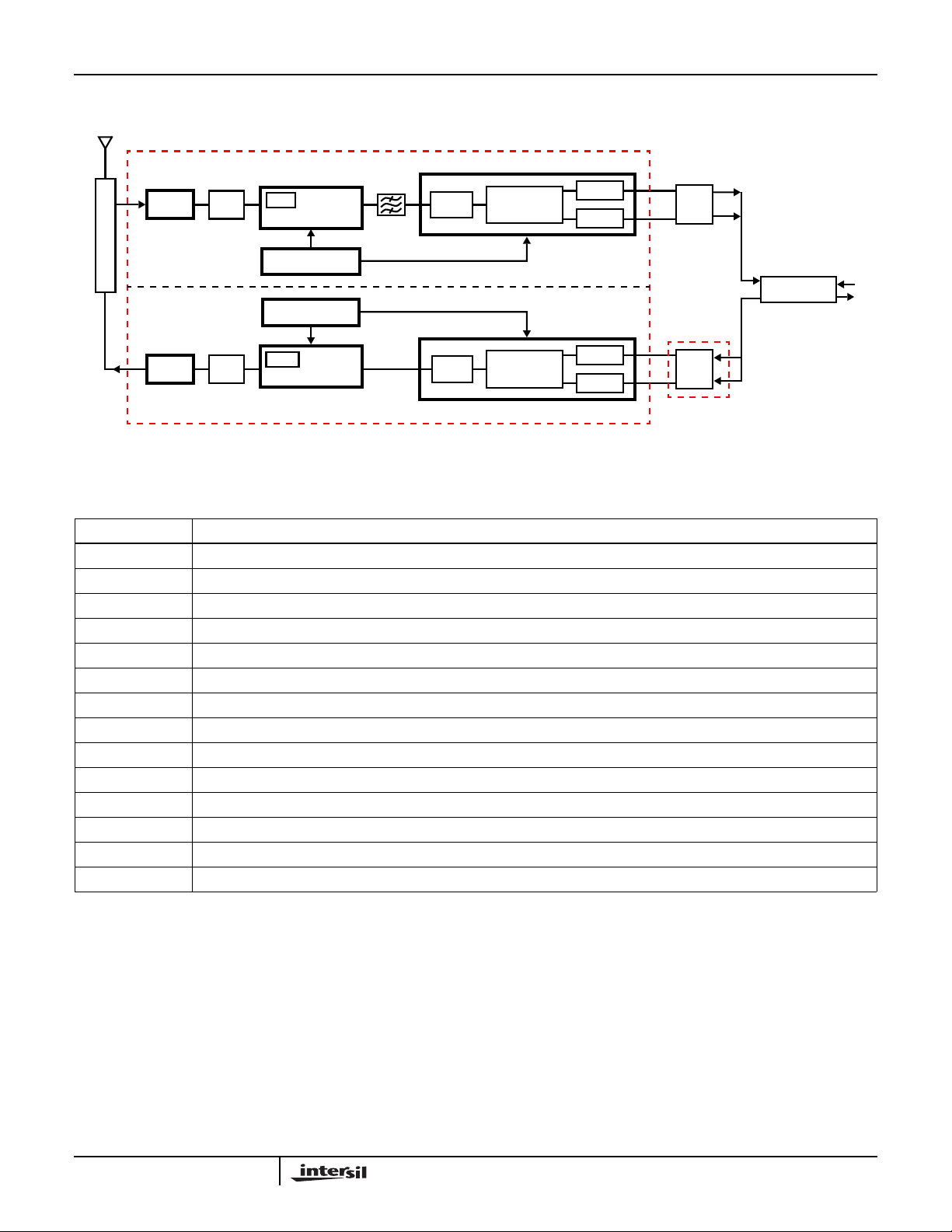
PRISM™ FULL DUPLEX CHIP SET
HFA3661
(FILE #4240)
LNA
CONVERTER
SYNTHESIZER
SYNTHESIZER
AGC
CONVERTER
HFA3663 (FILE #4241)
HFA3664 (FILE #4242)
D
U
P
L
E
X
E
R
HFA3424/21
(FILE #4131)
LNA BPF
HFA3925
(FILE #4132)
PA BPF
HFA3524
(FILE #4062)
HFA3524
(FILE #4062)
Pin Description
RF/IF
RF LO1
RF LO2
IF/RF
FILTER
HFA3663
IF AGC
IF LO1
IF LO2
AGC
HFA3761 (FILE #4236)
QMODEM
HFA3763
(FILE #4237)
QMODEM
LPF
A/D
LPF
BASEBAND
LPF
D/A
LPF
OPTIONAL WHEN IN
ANALOG MODE
PRISM™ FULL DUPLEX RADIO
CHIP SET, FILE #4238
NAME DESCRIPTION
LO_IN Local Oscillator Input.
LO_BY Local Oscillator Input Bypass (AC coupled to GND).
PRE_IN Power Pre-Amplifier Input.
PRE_OUT Power Pre-Amplifier Output.
PRE_VCC1 Power Pre-Amplifier 1st Stage Positive Power Supply. Use high quality RF decoupling capacitors.
PRE_VCC2 Power Pre-Amplifier 2nd Stage Positive Power Supply. Use high quality RF decoupling capacitors.
PRE_VCC3 Power Pre-Amplifier 3rd Stage Positive Power Supply. Use high quality RF decoupling capacitors.
BIAS_V
MIX_V
CC
CC
LO Buffer, Bias, Mixer and AGC Control Positive Power Supply. Requires an isolation coil to VCC.
Transmit Mixer Output Stage Positive Power Supply. Use high quality RF decoupling capacitors.
RX_PE Power Enable Control Input. Refer to the Power Control Truth Table.
TXM_RF Transmit Mixer RF Output.
IF_IN Transmit Mixer Positive IF Input. Requires external bias resistor to VCC.
IF_BY Transmit Mixer Negative IF Input (AC coupled to GND).
GND Circuit Ground Pins (Qty 6). Internally connected with the exception of pin 17.
2-202
 Loading...