HFA3624
Data Sheet November 1998 File Number
2.4GHz Up/Down Converter
™
The Intersil 2.4GHz PRISM™ chip set
is a highly integrated five-chip solution
for RF modems employing Direct
Sequence Spread Spectrum (DSSS)
signaling. The HFA3624 RF/IF
converter is one of the five chips in the PRISM™ chip set
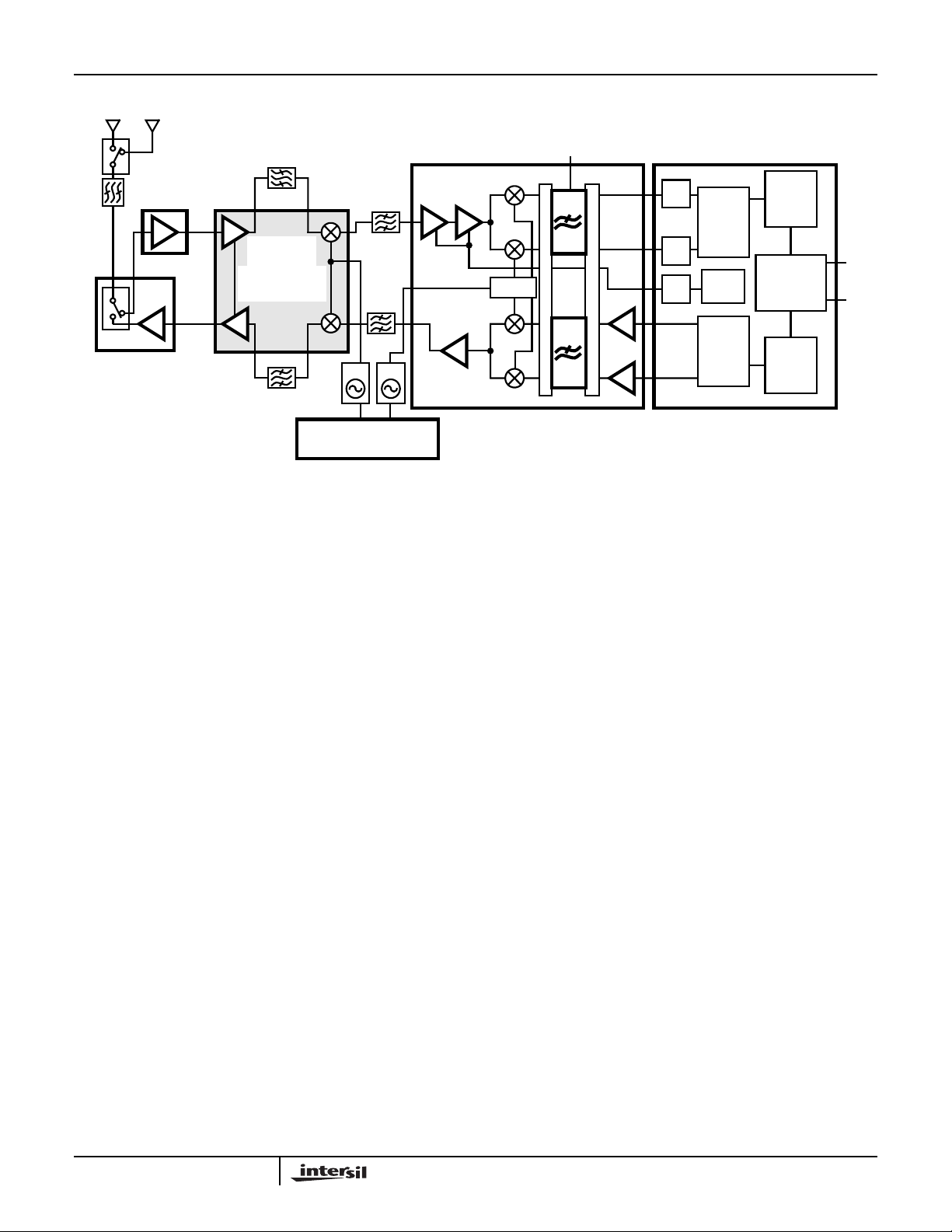
(see Figure 1 for the typical application circuit).
The HFA3624 Up/Downcon verter is a monolithic bipolar
device for up/do wn conversion applications in the 2.4GHz to
2.5GHz range. Manufactured in the Intersil UHF1X process ,
the device consists of a low noise amplifier and down
conversion mix er in the receive section and an up conversion
mixer with power preamp in the transmit section. An energy
saving power enable control feature assures isolation
between the receive and transmit circuits f or time division
multiplexedsystems.The devicerequires lowdrive levelsfrom
the local oscillator and is housed in a small outline 28 lead
SSOP package ideally suited for PCMCIA card applications.
4066.8
Features
• Complete Receive/Transmit Front End
• RF Frequency Range. . . . . . . . . . . . . . 2.4GHz to 2.5GHz
• IF Operation . . . . . . . . . . . . . . . . . . . . .10MHz to 400MHz
• Single Supply Battery Operation . . . . . . . . . 2.7V to 5.5V
• Independent Receive/Transmit Power Enable Mode
Applications
• Systems Targeting IEEE 802.11 Standard
• PCMCIA Wireless Transceiver
• Wireless Local Area Network Modems
• TDMA Packet Protocol Radios
• Part 15 Compliant Radio Links
• Portable Battery Powered Equipment
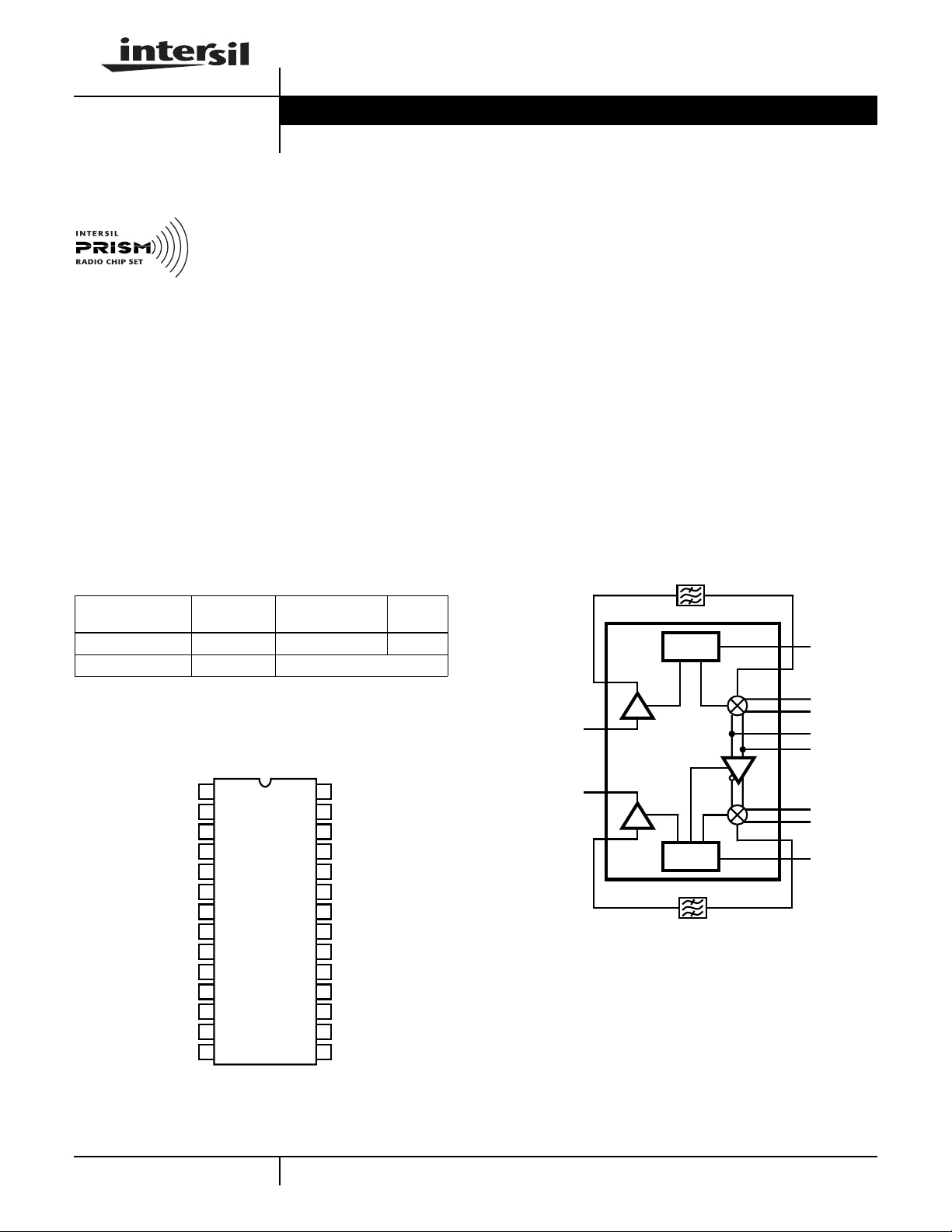
Block Diagram
Ordering Information
TEMP.
PART NUMBER
RANGE (oC) PACKAGE
HFA3624IA -40 to 85 28 Ld SSOP M28.15
HFA3624IA96 -40 to 85 Tape and Reel
PKG.
NO.
Pinout
HFA3624
(SSOP)
TOP VIEW
LNA_RX_V
GND
LNA_RX_OUT
GND
LNA_RX_V
GND
LNA_RX_IN
PRE_TX_OUT
GND
PRE_TX_V
GND
PRE_TX_IN
GND
PRE_TX_V
CC2
CC1
CC2
CC1
1
2
3
4
5
6
7
8
9
10
11
12
13
14
28
27
26
25
24
23
22
21
20
19
18
17
16
15
RX_PE
RX_V
CC
RXM_RF
GND
RXM_IF+
RXM_IFLO_BY
LO_IN
TXM_IFTXM_IF+
GND
TXM_RF
TX_V
CC
TX_PE
LNA_RX_OUT
LNA_RX_IN
PRE_TX_OUT
PRE_TX_IN
LNA
PRE
RX BIAS
RXM
TXM
TX BIAS
RX_PE
RXM_RF
RXM_IF+
RXM_IF-
LO_BY
LO_IN
LOB
TXM_IFTXM_IF+
TXM_RF
TX_PE
2-27
CAUTION: These devices are sensitive to electrostatic discharge; follow proper IC Handling Procedures.
http://www.intersil.com or 407-727-9207
PRISM® is a registered trademark of Intersil Corporation. PRISM logo is a trademark of Intersil Corporation.
| Copyright © Intersil Corporation 1999

HFA3624
HF A3424 (NOTE)
(FILE# 4131)
HF A3624
UP/DOWN
CONVERTER
(FILE# 4066)
RFPA
HF A3925
(FILE# 4132)
NOTE: Required for systems targeting 802.11 Specifications.
FIGURE 1. TYPICAL TRANSCEIVER APPLICATION CIRCUIT USING THE HFA3624
VCO
DUAL SYNTHESIZER
HFA3524
(FILE# 4062)
VCO
HFA3724
(FILE# 4067)
÷2
QUAD IF MODULATOR
0o/90
TUNE/SELECT
I
M
o
U
X
Q
HSP3824
(FILE# 4064)
RXI
RXQ
RSSI
M
U
X
A/D
DE-
SPREAD
A/D
CCA
A/D
TXI
SPREAD
TXQ
DSSS BASEBAND PROCESSOR
PRISM™ CHIP SET FILE #4063
DPSK
DEMOD
802.11
MAC-PHY
INTERFACE
DPSK
MOD.
DATA TO MACCTRL
For additional information on the PRISM™ chip set, call
(407) 724-7800to accessIntersil’ AnswerFAXsystem. When
prompted, key in the four-digit document number (File #) of
the datasheets you wish to receive.
The four-digit file numbers are shown in Figure 1, and
correspond to the appropriate circuit.
2-28

HFA3624
Absolute Maximum Ratings Thermal Information
Supply Voltage. . . . . . . . . . . . . . . . . . . . . . . . . . . . . . -0.3V to +6.0V
Voltage on Any Other Pin. . . . . . . . . . . . . . . . . . . -0.3 to VCC+0.3V
Operating Conditions
Supply Voltage Range. . . . . . . . . . . . . . . . . . . . . . . . . .2.7V to 5.5V
Temperature Range. . . . . . . . . . . . . . . . . . . . . . .-40oC ≤ TA≤ 85oC
CAUTION: Stresses above those listed in “Absolute Maximum Ratings” may cause permanent damage to the device. This is a stress only rating and operationofthe
device at these or any other conditions above those indicated in the operational sections of this specification is not implied.
NOTE:
1. θJA is measured with the component mounted on an evaluation PC board in free air.
Thermal Resistance (Typical, Note 1) θJA (oC/W)
28 Lead Plastic SSOP. . . . . . . . . . . . . . . . . . . . . . . 88
Package Power Dissipation at 70oC
28 Lead Plastic SSOP. . . . . . . . . . . . . . . . . . . . . . . . . . . . . .0.9W
Maximum Junction Temperature. . . . . . . . . . . . . . . . . . . . . . .150oC
Maximum Storage Temperature Range . . . . . ..-65oC ≤ TA≤ 150oC
Maximum Lead Temperature (Soldering 10s). . . . . . . . . . . . .300oC
(SSOP - Lead Tips Only)
Electrical Specifications V
PARAMETER SYMBOL TEMP (oC) MIN TYP MAX UNITS
LO INPUT CHARACTERISTICS (LO_IN = 2170MHz/-3dBm, RSLO = 50Ω, tested in both RX and TX modes, all unused inputs and
LO Input Frequency Range LO_f 25 2.0 - 2.49 GHz
LO Input Drive Level LO_dr 25 -6 -3 3 dBm
LO Input VSWR LO_SWR Full - 1.5 2.0:1 RECEIVE LNA CHARACTERISTICS (LNA_RX_IN = 2450MHz/-25dBm, RS = RL = 50Ω, Receive Mode)
Receive LNA Frequency Range LNA_f 25 2.4 - 2.5 GHz
LNA Noise Figure LNA_NF 25 - 3.5 - dB
LNA Power Gain LNA_PG Full 13.5 15.5 - dB
LNA Reverse Isolation (Source = 2450MHz/-25dBm) LNA_ISO 25 - 30 - dB
LNA Output 3rd Order Intercept
(LNA_RX_IN = 2449.9MHz, 2450.1MHz / -35dBm)
LNA Output 1dB Compression LNA_P1D 25 - 5.5 - dBm
LNA Input VSWR LNA_ISWR Full - 1.85:1 2.2:1 LNA Input Return Loss LNA_IRL Full - 10.5 8.5 dB
LNA Output VSWR LNA_OSWR Full - 1.6 2.0:1 LNA Output Return Loss LNA_ORL Full - 12.7 9.5 dB
RECEIVE MIXER CHARACTERISTICS (LO_IN = 2170MHz/-3dBm, RXM_RF = 2450MHz/-25dBm, RSLO = 50Ω, RSRF = 50Ω,
Mixer RF Frequency Range RXM_RFf 25 2.4 - 2.5 GHz
Mixer IF Frequency Range RXM_IFf 25 10 - 400 MHz
SSB Noise Figure (Note 3) RXM_NF 25 - 15 - dB
Mixer Power Conversion Gain (Note 2) RXM_PG 25 4 6 - dB
Mixer IF Output 3rd Order Intercept
(RXM_RF = 2449.9MHz, 2450.1MHz/-30dBm)
Mixer IF Output 1dB Compression RXM_P1D 25 - -5 - dBm
Mixer RF Input VSWR (2.4GHz to 2.5GHz) RXM_SWR 25 - 1.5:1 2.0:1 Mixer RF Input Return Loss RXM_IRL 25 - 14.0 9.5 dB
IF Open Collector Output Resistance (IF = 280MHz) RXM_ROUT 25 - 1.5 - kΩ
IF Open Collector Output Capacitance RXM_COUT 25 - 0.4 - pF
= +2.7V, LO = 2170MHz, IF = 280MHz, RF = 2450MHz, ZO=50Ω,
CC
Unless Otherwise Specified
outputs are terminated into 50Ω)
LNA_IP3 25 - 18 - dBm
RLIF = 50Ω with external matching network (Note 2), Receive Mode)
85 3 - - dB
RXM_IP3 25 - 4.0 - dBm
2-29

HFA3624
Electrical Specifications V
PARAMETER SYMBOL TEMP (oC) MIN TYP MAX UNITS
Mixer LO to RF Isolation RXA_LOR 25 - 22 - dB
RECEIVE LNA/MIXER CASCADED CHARACTERISTICS (-3dB Loss RF Image Filter between LNA and Mixer, LNA_RX_IN = 2450MHz/-
Cascaded Noise Figure CRX_NF 25 - 6.24 - dB
Cascaded Power Gain CRX_PG 25 15 18 - dB
Cascaded Input IP3 CRX_IP3 25 - -14.1 - dBm
Cascaded Input Compression Point CRX_P1D 25 - -23.2 - dBm
Maximum Input Power
(Output may be gain compressed, but functional)
TRANSMIT MIXER CHARACTERISTICS (LO_IN = 2170MHz/-3dBm, TXM_IF+ = 280MHz/-13dBm, RSIF = 50Ω, RSLO = 50Ω,
IF Input Frequency Range TXM_IFf 25 10 - 400 MHz
IF Input Resistance (IF = 280MHz) TXM_RIN 25 - 3 - kΩ
IF Input Capacitance (IF = 280MHz) TXM_CIN 25 - 0.5 - pF
Power Conversion Gain (RSIF = 50Ω) TXM_PG50 25 -6 -3.4 - dB
Power Conversion Gain (RSIF = 250Ω) (Notes 4, 5) TXM_PG250 25 -0.5 2.1 - dB
Transmit Mixer LO Leakage TXM_LEAK 25 - -20 -18 dBm
RF Output Frequency Range TXM_RFf 25 2.4 - 2.5 GHz
TXM_RF VSWR (2.4GHz to 2.5GHz) TXM_OSWR Full - 1.5 2.0:1 TXM_RF Return Loss TXM_ORL Full - 14 9.5 dB
Mixer Output 1dB Compression TXM_P1D 25 - -10.5 - dBm
Output SSB Noise Figure (RSIF = 50Ω) TXM_NF50 25 - 18.3 - dB
Output 3rd Order Intercept (RSIF = 50Ω) TXM_IP3_50 25 - 1.1 - dBm
Output SSB Noise Figure (RSIF = 250Ω) TXM_NF250 25 - 14.5 - dB
Output 3rd Order Intercept (RSIF = 250Ω) TXM_IP3_250 25 - -1.5 - dBm
TRANSMIT POWER PRE-AMP CHARACTERISTICS (PRE_IN = 2450MHz/-13dBm, RS = RL = 50Ω, Transmit Mode)
Power Pre-Amp Frequency Range PRE_f 25 2.4 - 2.5 GHz
Power Gain PRE_PG 25 10.8 12.3 - dB
PRE_AMP Output 1dB Compression PRE_P1D 25 5.0 5.6 - dBm
PRE_AMP Noise Figure PRE_NF 25 - 5.7 - dB
PRE_AMP Output 3rd Order Intercept PRE_IP3 25 - 15.3 - dBm
PRE_AMP Input VSWR (2.4GHz to 2.5GHz) PRE_ISWR Full - 1.3:1 2.0:1 PRE_AMP Input Return Loss PRE_IRL Full - 17.7 9.5 dB
PRE_AMP Output VSWR (2.4GHz to 2.5GHz) PRE_OSWR Full - 1.3:1 2.0:1 PRE_AMP Output Return Loss PRE_ORL Full - 17.7 9.5 dB
= +2.7V, LO = 2170MHz, IF = 280MHz, RF = 2450MHz, ZO=50Ω,
CC
Unless Otherwise Specified (Continued)
25dBm, RLIF = 250Ω external matching network, (Note 6))
85 14 - - dB
CRX_dr 25 - +3 - dBm
RLRF = 50Ω, Transmit Mode)
85 -7.5 - - dB
85 -2 - - dB
85 7.8 - - dB
2-30

HFA3624
Electrical Specifications V
PARAMETER SYMBOL TEMP (oC) MIN TYP MAX UNITS
TRANSMIT MIXER/POWER PRE-AMP CASCADED CHARACTERISTICS (TXM_IF+ =280MHz/-13dBm, -3dBLoss RFImage Filterwith no LO
Cascaded Power Gain CTX_PG 25 8 11.4 - dB
Cascaded Output P1dB CTX_P1D 25 - -2.0 - dBm
Cascaded Output NF CTX_NF 25 - 15 - dB
Cascaded Output 3rd Order Intercept CTX_IP3 25 - 7.1 - dBm
Cascaded LO Leakage CTX_LEAK 25 - -8.7 - dBm
POWER SUPPLY AND LOGIC CHARACTERISTICS
Voltage Supply Range V
Transmit Mode Supply Current (VCC = 2.7V) TX_2.7I
Receive Mode Supply Current (VCC = 2.7V) RX_I
Power Down Current (VCC = 5.5V) ICC_PD Full - 0.3 10 µA
Logic Input Low Level V
Logic Input High Level V
Logic Low Input Bias Current (VPE = 0V, VCC = 5.5V) IB_LO Full - - 1 µA
Logic High Input Bias Current (VPE = 5.5V, VCC = 5.5V) IB_HI Full - - 150 µA
TX/RX Power Enable Time (Note 7) PEt Full - 0.25 1 µs
TX/RX Power Disable Time (Note 7) PDt Full - 0.25 1 µs
NOTES:
2. See Figure 5 Test Circuit for 50Ω IF matching network component values.
3. SSB (Single SideBand)NoiseFiguremeasurement requires the useofanIF Reject/Highpass Filter betweentheNoiseSource and the RXM_RF
port. This filter prevents IF input noise from interfering with the Mixer IF output Noise Figure Measurement.
4. Transmit mixer measured with Impedance Transform Network 250Ω at device to 50Ω at the source. Refer to Figure 5, pin 19.
5. Implied limit, production measurement uses 50Ω termination at pin 19 (RSIF=50Ω). Typical transmit conversion gain increase of 5.5dB with
application circuit Figure 5 (RSIF = 250Ω).
6. See Figure 2 for Typical Application Circuit.
7. Enable/Disable Time Specifications are tested with the external component values shown in the Figure 5 Test Circuit, with an IF frequency of
280MHz. Specifically the AC coupling capacitors on the TXM_IF+ and TXM_IF- pins are biased up to operating voltage from a fixed internal
current source at power up. Increasing these AC coupling capacitors above 1000pF will slow Enable Time proportionately.
= +2.7V, LO = 2170MHz, IF = 280MHz, RF = 2450MHz, ZO=50Ω,
CC
Unless Otherwise Specified (Continued)
suppression between Mixer and Transmit Amp, RL = 50Ω, RSIF =
250Ω (Note 6))
85 5.5 - - dB
CC
CC
CC
IL
IH
25 2.7 - 5.5 V
25 32 49 57 mA
85 43 - 64 mA
25 10 18 20.5 mA
85 19 22.5 24 mA
Full -0.2 - 0.8 V
Full 2.0 - V
CC
V
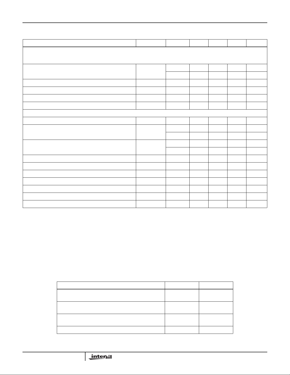
POWER CONTROL TRUTH TABLE
STATE RX_PE TX_PE
Power Down
(Receive/Transmit Channels Power Down)
Transmit Mode
(Receive Channel Power Down)
Receive Mode
(Transmit Channel Power Down)
Not Recommended High High
Low Low
Low High
High Low
2-31

HFA3624
Pin Descriptions
PINS SYMBOL DESCRIPTION
1 LNA_RX_V
3 LNA_RX_OUT Receive Channel Low Noise Amplifier Output (2400MHz to 2500MHz). The nominal impedance of 50Ω,
5 LNA_RX_V
7 LNA_RX_IN Receive Channel Low Noise Amplifier Input (2400MHz to 2500MHz). The nominal impedance of 50Ω,over
8 PRE_TX_OUT Transmit Channel Power Pre-Amplifier Output (2400MHz to 2500MHz). The nominal impedance of 50Ω,
10 PRE_TX_V
12 PRE_TX_IN TransmitChannel Power Pre-Amplifier Input (2400MHz to 2500MHz). The nominal impedanceof 50Ω,over
14 PRE_TX_V
15 TX_PE Transmit Channel Power Enable Control Input. TTL compatible input. Refer to “Power Control Truth Table”
16 TX_V
17 TXM_RF Transmit Channel Mixer RF Output (2400MHz to 2500MHz). The nominal impedance of 50Ω, over the op-
19 TXM_IF+ Transmit Channel Mixer IF+ Input (10MHz to 400MHz). The TXM_IF+ and TXM_IF- pins form a high input
20 TXM_IF- Transmit Channel Mixer IF- Input (10MHz to 400MHz). The TXM_IF+ and TXM_IF- pins form a high input
21 LO_IN Local Oscillator Input (2000MHz to 2490MHz). The LO_IN and LO_BY pins form a differential pair with a
22 LO_BY Local Oscillator Input Bypass (2000MHz to 2490MHz). The LO_IN and LO_BY pins form a differential pair
CC
Receive Channel LowNoise Amplifier Output Stage Positive Power Supply.Use highquality decouplingca-
CC2
pacitors right at the pin. A 5pF chip capacitor is recommended.
over the operating frequency range, is achieved with an on chip narrowband tuned circuit. This pinrequires
AC coupling.
Receive Channel Low Noise Amplifier Input Stage Positive Power Supply. Use high quality decoupling ca-
CC1
pacitors right at the pin. A 200pF chip capacitor is recommended.
the operating frequency range,is achieved with an on chip narrowband tuned circuit. This pin requires AC
coupling.
overthe operatingfrequency range,is achieved with on chip narrowband tuned circuit. This pin requiresAC
coupling.
TransmitChannel Power Pre-Amplifier OutputStage PositivePowerSupply.Use highquality decoupling ca-
CC2
pacitors right at the pin. A 200pF chip capacitor is recommended.
the operating frequency range,is achieved with an on chip narrowband tuned circuit. This pin requires AC
coupling.
Transmit Channel Power Pre-Amplifier Input Stage Positive Power Supply. Use high quality decoupling ca-
CC1
pacitors right at the pin. A 200pF chip capacitor is recommended.
on previous page.
Transmit Channel Positive Power Supply. Use high quality decoupling capacitors right at the pin. A 200pF
chip capacitor is recommended.
erating frequency range, is achieved with an on chip narrowband tuned circuit. This pin requires AC coupling.
impedance differential pair. Either input (or both inputs for special applications) may be used for the IF signal. Typically the TXM_IF- pin is bypassed to ground with a 470pF capacitor and the TXM_IF+ pin is AC
coupled tothe transmit IF signal. The high impedance input requires external termination. The specified input impedance is modeled as a resistor in parallel with a capacitor derived from S parameters at 280MHz.
The input Impedance will increase at lower IF frequencies.
This pin requires AC coupling. Increasing the AC coupling capacitor to larger than 1000pF will degrade
Transmit Enable Time.
impedance differential pair. Either input (orboth forspecial applications) may be used for the IF signal.Typically theTXM_IF- pin is bypassed toground with a 470pF capacitor and the TXM_IF+pin is AC coupled to
the transmit IF signal. The high impedance input requires external termination. The specified input impedance is modeled as a resistor in parallel with a capacitor derived from S parameters at 280MHz. The input
impedance will increase at lower IF frequencies.
This pin requires AC coupling. Increasing the AC coupling capacitor to larger than 1000pF will degrade
Transmit Enable Time.
mutual broadband 50Ω impedance. Refer to the LO_BY pin for details. The recommended LO power is 3dBm, however usable performance is obtained for therange -6dBmto +3dBm.The LO_INpin requires AC
coupling.
with a mutual broadband 50Ω input impedance. The LO_BY pin can be used as a signal input, but may
have slightly degraded performance due to a clamp circuit to GND. Typicallythe LO_BY pin is bypassed to
GND with a 5pF capacitor. The LO_BY pin requires AC coupling.
2-32
 Loading...