

HFA3102
Data Sheet August 1996 File Number 3635.2
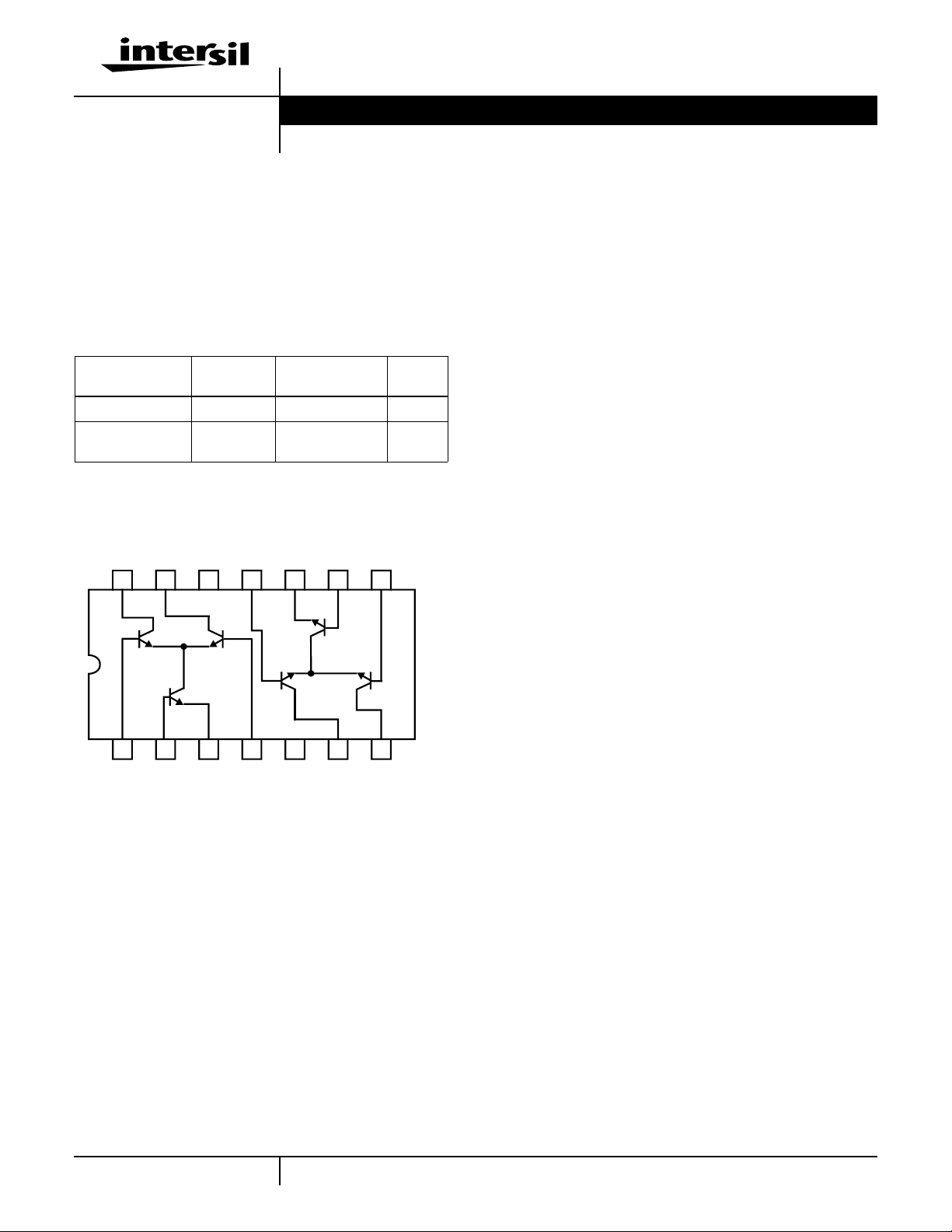
Dual Long-Tailed Pair Transistor Array
The HFA3102 is an all NPN transistor array configured as
dual differential amplifiers with tail transistors. Based on
Intersil bonded wafer UHF-1 SOI process, this array
achieves very high f
h
and VBE matching characteristics over temperature.
FE
(10GHz) while maintaining excellent
T
Collector leakage currents are maintained to under 0.01nA.
Ordering Information
TEMP.
PART NUMBER
HFA3102B -40 to 85 14 Ld SOIC M14.15
HFA3102B96 -40 to 85 14 Ld SOIC Tape
RANGE (oC) PACKAGE
and Reel
PKG.
NO.
M14.15
Pinout/Functional Diagram
HFA3102
(SOIC)
TOP VIEW
14 13 12 11 10 9 8
Q
Q
Q
1
2
6
Features
• High Gain-Bandwidth Product (fT) . . . . . . . . . . . . . 10GHz
• High Power Gain-Bandwidth Product. . . . . . . . . . . . 5GHz
• High Current Gain (h
) . . . . . . . . . . . . . . . . . . . . . . . 70
FE
• Noise Figure (Transistor) . . . . . . . . . . . . . . . . . . . . . 3.5dB
• Low Collector Leakage Current . . . . . . . . . . . . . <0.01nA
• Excellent h
and VBE Matching
FE
• Pin-to-Pin to UPA102G
Applications
• Single Balanced Mixers
• Wide Band Amplification Stages
• Differential Amplifiers
• Multipliers
• Automatic Gain Control Circuits
• Frequency Doublers, Tripplers
• Oscillators
• Constant Current Sources
• Wireless Communication Systems
Q
Q
4
Q
3
1234567
5
• Radio and Satellite Communications
• Fiber Optic Signal Processing
• High Performance Instrumentation
3-449
CAUTION: These devices are sensitive to electrostatic discharge; follow proper IC Handling Procedures.
1-888-INTERSIL or 321-724-7143
| Copyright © Intersil Corporation 1999

HFA3102
Absolute Maximum Ratings T
V
Collector to Emitter Voltage. . . . . . . . . . . . . . . . . . . . . . . 8.0V
CEO
V
Collector to Base Voltage . . . . . . . . . . . . . . . . . . . . . . . 12.0V
CBO
V
Emitterr to Base Voltage . . . . . . . . . . . . . . . . . . . . . . . . 12.0V
EBO
IC, Collector Current . . . . . . . . . . . . . . . . . . . . . . . . . . . . . . . . 30mA
=25oC Thermal Information
A
Thermal Resistance (Typical, Note 1) θJA (oC/W)
SOIC Package . . . . . . . . . . . . . . . . . . . . . . . . . . . . . 125
Maximum Power Dissipation at 75oC
Any One Transistor. . . . . . . . . . . . . . . . . . . . . . . . . . . . . . . .0.25W
Maximum Junction Temperature (Die) . . . . . . . . . . . . . . . . . . . .175oC
Operating Conditions
Temperature Range. . . . . . . . . . . . . . . . . . . . . . . . . . -40oC to 85oC
Maximum Junction Temperature (Plastic Package) . . . . . . . .150oC
Maximum Storage Temperature Range. . . . . . . . . . -65oC to 150oC
Maximum Lead Temperature (Soldering 10s) . . . . . . . . . . . . .300oC
(SOIC - Lead Tips Only)
CAUTION: Stresses above those listed in “Absolute Maximum Ratings” may cause permanent damage to the device. This is a stress only rating and operation of the
device at these or any other conditions above those indicated in the operational sections of this specification is not implied.
NOTE:
1. θJA is measured with the component mounted on an evaluation PC board in free air.
Electrical Specifications T
= 25oC
A
(NOTE 2)
ALL GRADES
TEST
SYMBOLS PARAMETER TEST CONDITIONS
V
(BR)CBO
Collector-to-Base Breakdown Voltage
IC = 100µA, IE = 0 A 12 18 - V
LEVEL
UNITSMIN TYP MAX
(Q1, Q2, Q4, and Q5)
V
(BR)CEO
Collector-to-Emitter Breakdown
IC = 100µA, IB = 0 A 8 12 - V
Voltage (Q1 thru Q6)
V
(BR)EBO
Emitter-to-Base Breakdown Voltage (Q
IE = 50µA, IC = 0 A 5.5 6 - V
3
and Q6)
I
CBO
I
EBO
h
FE
C
CB
C
EB
f
T
f
MAX
G
NFMIN
NF
MIN
NF
50Ω
h
FE1/hFE2
V
OS
Collector Cutoff Current
VCB = 5V, IE = 0 A - 0.1 10 nA
(Q1, Q2, Q4, and Q5)
Emitter Cutoff Current (Q3 and Q6)V
DC Current Gain (Q1 thru Q6)I
= 1V, IC = 0 A - - 100 nA
EB
= 10mA, VCE = 3V A 40 70 - -
C
Collector-to-Base Capacitance VCB = 5V, f = 1MHz B - 300 - fF
Emitter-to-Base Capacitance VEB = 0, f = 1MHz B - 200 - fF
Current Gain-Bandwidth Product IC = 10mA, VCE = 5V C - 10 - GHz
Power Gain-Bandwidth Product IC = 10mA, VCE = 5V C - 5 - GHz
Availab le Gain at Minimum Noise Figure IC = 3mA,
f = 0.5GHz C - 17.5 - dB
VCE = 3V
f = 1.0GHz C - 12.4 - dB
Minimum Noise Figure IC = 3mA,
f = 0.5GHz C - 1.8 - dB
VCE = 3V
f = 1.0GHz C - 2.1 - dB
50Ω Noise Figure IC = 3mA,
f = 0.5GHz C - 3.3 - dB
VCE = 3V
f = 1.0GHz C - 3.5 - dB
DC Current Gain Matching
IC = 10mA, VCE = 3V A 0.9 1.0 1.1 -
(Q1 and Q2, Q4 and Q5)
Input Offset Voltage (Q1 and Q2),
IC = 10mA, VCE = 3V A - 1.5 5 mV
(Q4 and Q5)
I
OS
Input Offset Current (Q1 and Q2),
IC = 10mA, VCE = 3V A - 5 25 µA
(Q4 and Q5)
3-450

HFA3102
Electrical Specifications T
SYMBOLS PARAMETER TEST CONDITIONS
dVOS/dT Input Offset Voltage TC
(Q1 and Q2, Q4 and Q5)
I
TRENCH-
LEAKAGE
NOTE:
2. Test Level: A. Production Tested; B. Typical or Guaranteed Limit Based on Characterization; C. Design Typical for Information Only
Collector-to-Collector Leakage
(Pin 6, 7, 13, and 14)
= 25oC (Continued)
A
(NOTE 2)
TEST
LEVEL
IC = 10mA, VCE = 3V C - 0.5 - µV/oC
∆V
= 5V B - 0.01 - nA
TEST
ALL GRADES
PSPICE Model for a Single Transistor
.Model NUHFARRY NPN
+ ( IS= 1.840E-16 XTI= 3.000E+00 EG= 1.110E+00 VAF= 7.200E+01
+ VAR= 4.500E+00 BF= 1.036E+02 ISE= 1.686E-19 NE= 1.400E+00
+ IKF= 5.400E-02 XTB= 0.000E+00 BR= 1.000E+01 ISC= 1.605E-14
+ NC= 1.800E+00 IKR= 5.400E-02 RC= 1.140E+01 CJC= 3.980E-13
+ MJC= 2.400E-01 VJC= 9.700E-01 FC= 5.000E-01 CJE= 2.400E-13
+ MJE= 5.100E-01 VJE= 8.690E-01 TR= 4.000E-09 TF= 10.51E-12
UNITSMIN TYP MAX
+ ITF= 3.500E-02 XTF= 2.300E+00 VTF= 3.500E+00 PTF= 0.000E+00
+ XCJC= 9.000E-01 CJS= 1.689E-13 VJS= 9.982E-01 MJS= 0.000E+00
+ RE= 1.848E+00 RB= 5.007E+01 RBM= 1.974E+00 KF= 0.000E+00
+ AF= 1.000E+00)
3-451

HFA3102
Common Emitter S-Parameters
VCE = 5V and IC = 5mA
FREQ. (Hz) |S11| PHASE(S11)|S
1.0E+08 0.833079 -11.7873 1.418901E-02 78.8805 11.0722 168.576 0.976833 -11.0509
2.0E+08 0.791776 -22.8290 2.695740E-02 68.6355 10.5177 157.897 0.930993 -21.3586
3.0E+08 0.734911 -32.6450 3.750029E-02 59.5861 9.75379 148.443 0.868128 -30.4451
4.0E+08 0.672811 -41.0871 4.572138E-02 51.9018 8.91866 140.361 0.799886 -38.1641
5.0E+08 0.612401 -48.2370 5.194147E-02 45.5043 8.10511 133.569 0.734033 -44.5998
6.0E+08 0.557126 -54.2780 5.659943E-02 40.2112 7.35944 127.882 0.674392 -49.9370
7.0E+08 0.508133 -59.4102 6.009507E-02 35.8226 6.69712 123.102 0.622181 -54.3777
8.0E+08 0.465361 -63.8123 6.274213E-02 32.1594 6.11750 119.047 0.577269 -58.1022
9.0E+08 0.428238 -67.6313 6.477134E-02 29.0743 5.61303 115.571 0.538952 -61.2587
1.0E+09 0.396034 -70.9834 6.634791E-02 26.4506 5.17405 112.556 0.506365 -63.9647
1.1E+09 0.368032 -73.9591 6.758932E-02 24.1974 4.79104 109.913 0.478663 -66.3116
1.2E+09 0.343589 -76.6285 6.857937E-02 22.2441 4.45546 107.570 0.455091 -68.3702
1.3E+09 0.322155 -79.0462 6.937837E-02 20.5358 4.15997 105.472 0.435008 -70.1958
1.4E+09 0.303268 -81.2548 7.003020E-02 19.0293 3.89845 103.576 0.417872 -71.8314
1.5E+09 0.286542 -83.2880 7.056718E-02 17.6908 3.66577 101.849 0.403238 -73.3108
1.6E+09 0.271660 -85.1723 7.101343E-02 16.4930 3.45770 100.262 0.390735 -74.6609
1.7E+09 0.258359 -86.9292 7.138717E-02 15.4143 3.27074 98.7956 0.380056 -75.9030
1.8E+09 0.246420 -88.5759 7.170231E-02 14.4370 3.10197 97.4307 0.370947 -77.0544
1.9E+09 0.235659 -90.1265 7.196964E-02 13.5469 2.94897 96.1533 0.363195 -78.1288
2.0E+09 0.225923 -91.5925 7.219757E-02 12.7319 2.80969 94.9515 0.356623 -79.1377
2.1E+09 0.217085 -92.9836 7.239274E-02 11.9824 2.68243 93.8156 0.351081 -80.0903
2.2E+09 0.209034 -94.3076 7.256046E-02 11.2901 2.56573 92.7373 0.346442 -80.9942
2.3E+09 0.201678 -95.5713 7.270498E-02 10.6480 2.45837 91.7097 0.342599 -81.8557
2.4E+09 0.194939 -96.7803 7.282977E-02 10.0503 2.35928 90.7271 0.339458 -82.6802
2.5E+09 0.188747 -97.9395 7.293764E-02 9.49212 2.26756 89.7844 0.336942 -83.4719
2.6E+09 0.183044 -99.0530 7.303093E-02 8.96908 2.18243 88.8775 0.334982 -84.2347
2.7E+09 0.177780 -100.124 7.311157E-02 8.47753 2.10322 88.0026 0.333518 -84.9716
2.8E+09 0.172909 -101.156 7.318117E-02 8.01430 2.02934 87.1565 0.332499 -85.6853
2.9E+09 0.168394 -102.152 7.324107E-02 7.57661 1.96027 86.3366 0.331879 -86.3781
3.0E+09 0.164200 -103.114 7.329243E-02 7.16204 1.89556 85.5404 0.331620 -87.0518
VCE = 5V and IC = 10mA
FREQ. (Hz) |S11| PHASE(S11)|S
1.0E+08 0.728106 -16.4319 1.273920E-02 75.4177 15.1273 165.227 0.959692 -14.2688
2.0E+08 0.670836 -31.2669 2.342300E-02 62.8941 13.9061 152.045 0.886232 -26.9507
3.0E+08 0.600268 -43.7663 3.132521E-02 52.5891 12.3970 141.185 0.796016 -37.3172
4.0E+08 0.531768 -54.0028 3.681579E-02 44.5019 10.9257 132.570 0.708892 -45.4503
5.0E+08 0.471795 -62.3880 4.057046E-02 38.2308 9.62995 125.781 0.633146 -51.7704
6.0E+08 0.421506 -69.3569 4.316292E-02 33.3405 8.53559 120.378 0.570209 -56.7206
7.0E+08 0.379961 -75.2612 4.499071E-02 29.4764 7.62375 116.005 0.518803 -60.6598
8.0E+08 0.345693 -80.3608 4.631140E-02 26.3755 6.86423 112.398 0.476987 -63.8540
9.0E+08 0.317301 -84.8420 4.728948E-02 23.8481 6.22797 109.365 0.442915 -66.4948
1.0E+09 0.293608 -88.8381 4.803091E-02 21.7581 5.69057 106.771 0.415044 -68.7193
1.1E+09 0.273680 -92.4452 4.860515E-02 20.0070 5.23257 104.518 0.392146 -70.6269
1.2E+09 0.256782 -95.7336 4.905871E-02 18.5224 4.83873 102.532 0.373261 -72.2899
1.3E+09 0.242344 -98.7555 4.942344E-02 17.2505 4.49716 100.759 0.357640 -73.7620
1.4E+09 0.229918 -101.551 4.972158E-02 16.1506 4.19854 99.1602 0.344698 -75.0832
1.5E+09 0.219152 -104.150 4.996903E-02 15.1915 3.93554 97.7028 0.333974 -76.2840
1.6E+09 0.209767 -106.577 5.017730E-02 14.3490 3.70234 96.3629 0.325102 -77.3877
1.7E+09 0.201539 -108.851 5.035491E-02 13.6040 3.49428 95.1215 0.317789 -78.4122
1.8E+09 0.194288 -110.988 5.050825E-02 12.9411 3.30758 93.9633 0.311800 -79.3715
1.9E+09 0.187867 -113.001 5.064218E-02 12.3482 3.13919 92.8761 0.306940 -80.2768
2.0E+09 0.182157 -114.902 5.076045E-02 11.8151 2.98658 91.8500 0.303051 -81.1365
2.1E+09 0.177056 -116.698 5.086598E-02 11.3338 2.84766 90.8766 0.300003 -81.9578
2.2E+09 0.172484 -118.399 5.096107E-02 10.8974 2.72068 89.9494 0.297686 -82.7460
2.3E+09 0.168370 -120.012 5.104755E-02 10.5001 2.60420 89.0626 0.296007 -83.5057
2.4E+09 0.164656 -121.542 5.112690E-02 10.1373 2.49697 88.2115 0.294889 -84.2405
2.5E+09 0.161293 -122.996 5.120031E-02 9.80479 2.39793 87.3920 0.294266 -84.9533
2.6E+09 0.158239 -124.378 5.126876E-02 9.49919 2.30619 86.6007 0.294081 -85.6466
2.7E+09 0.155458 -125.694 5.133304E-02 9.21750 2.22098 85.8348 0.294285 -86.3223
2.8E+09 0.152919 -126.947 5.139381E-02 8.95716 2.14162 85.0916 0.294836 -86.9822
2.9E+09 0.150595 -128.140 5.145164E-02 8.71595 2.06753 84.3690 0.295696 -87.6275
3.0E+09 0.148463 -129.279 5.150697E-02 8.49194 1.99820 83.6651 0.296834 -88.2595
| PHASE(S12)|S21| PHASE(S21)|S22| PHASE(S22)
12
| PHASE(S12)|S21| PHASE(S21)|S22| PHASE(S22)
12
3-452

Typical Performance Curves
HFA3102
12
IB = 150µA
10
I
= 120µA
B
8
= 90µA
I
B
6
(mA)
C
I
= 60µA
I
B
4
IB = 30µA
2
0
012345
VCE (V)
FIGURE 1. IC vs V
0
10
CE
VCE = 3V
-2
10
-4
10
(A)
B
-6
10
AND I
C
I
-8
10
-10
10
-12
10
0.4 0.6 0.8 1.0
VBE (V)
140
120
100
80
FE
h
60
40
20
12
10
8
6
(GHz)
T
f
4
2
0
10
0
10
-4
-10
-8
10
FIGURE 2. hFE vs I
VCE = 5V
-6
10
-4
10
-2
10
0
10
IC (A)
C
-3
10
IC (A)
-2
10
-1
10
FIGURE 3. GUMMEL PLOT FIGURE 4. fT vs I
4.8
4.6
4.4
4.2
4.0
3.8
NOISE FIGURE (dB)
3.6
3.4
3.2
0 0.5 1.0 1.5 2.0 2.5 3.0
FREQUENCY (GHz)
20
18
16
14
12
| (dB)
21
|S
10
8
6
4
40
20
0
-20
-40
-60
, OUTPUT POWER (dBm)
OUT
-80
P
-100
-30 -20 -10 0 10
FIGURE 5. GAIN AND NOISE FIGURE vs FREQUENCY FIGURE 6. P
3-453
C
3rd ORDER INTERCEPT POINT
1dB COMPRESSION POINT
3RD ORDER PRODUCTS
, INPUT POWER (dBm)
P
IN
AND 3RD ORDER INTERCEPT
1dB
VCE = 5V
I
= 10mA
C
f = 1GHz
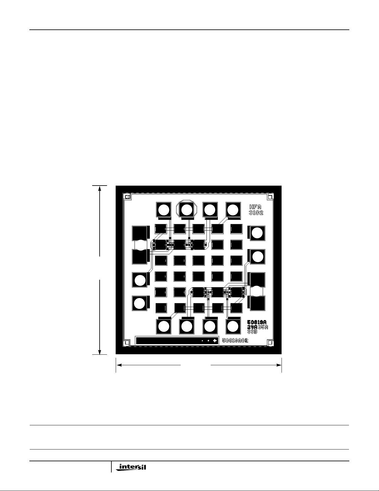
Die Characteristics
HFA3102
PROCESS:
UHF-1
DIE DIMENSIONS:
53 mils x 52 mils x 14 mils
1340µm x 1320µm x 355.6µm
METALIZATION:
Type: Metal 1: AlCu(2%)/TiW
Thickness: Metal 1: 8k
Å ±0.5kÅ
Type: Metal 2: AlCu(2%)
Thickness: Metal 2: 16k
Å ±0.8kÅ
Metallization Mask Layout
2
HFA3102
TOP VIEW
1 14
PASSIVATION:
Type: Nitride
Thickness: 4k
Å ±0.5kÅ
SUBSTRATE POTENTIAL (Powered Up):
Floating
13
1340µm
(53 mils)
12
3
11
4
10
5
9876
1320µm
(52 mils)
Pad numbers correspond to the 14 pin SOIC pinout.
All Intersil semiconductor products are manufactured, assembled and tested under ISO9000 quality systems certification.
Intersil semiconductor products are sold by description only. Intersil Corporation reserves the right to make changes in circuit design and/or specifications at any time without notice. Accordingly, the reader is cautioned to verify that data sheets are current before placing orders. Information furnished by Intersil is believed to be accurate and
reliable. However, no responsibility is assumed by Intersil or its subsidiaries for its use; nor for any infringements of patents or other rights of third parties which may result
from its use. No license is granted by implication or otherwise under any patent or patent rights of Intersil or its subsidiaries.
For information regarding Intersil Corporation and its products, see web site http://www.intersil.com
3-454
 Loading...