

Page 1
®
HFA3101
Data Sheet September 2004
Gilbert Cell UHF Transistor Array
The HFA3101 is an all NPN transistor array configured as a
Multiplier Cell. Based on Intersil’s bonded wafer UHF-1 SOI
process, this array achieves very high f
maintaining excellent h
and VBE matching characteristics
FE
(10GHz) while
T
that have been maximized through careful attention to circuit
design and layout, making this product ideal for
communication circuits. For use in mixer applications, the
cell provides high gain and good cancellation of 2nd order
distortion terms.
Ordering Information
PART NUMBER
(BRAND)
HFA3101B
(H3101B)
HFA3101BZ
(H3101B) (Note)
HFA3101B96
(H3101B)
HFA3101BZ96
(H3101B) (Note)
NOTE: Intersil Pb-free products employ special Pb-free material
sets; molding compounds/die attach materials and 100% matte tin
plate termination finish, which is compatible with both SnPb and
Pb-free soldering operations. Intersil Pb-free products are MSL
classified at Pb-free peak reflow temperatures that meet or exceed
the Pb-free requirements of IPC/JEDEC J STD-020C.
TEMP.
RANGE (°C)
-40 to 85 8 Ld SOIC M8.15
-40 to 85 8 Ld SOIC
-40 to 85 8 Ld SOIC Tape
-40 to 85 8 Ld SOIC Tape
PACKAGE
M8.15
(Pb-free)
M8.15
and Reel
M8.15
and Reel (Pb-free)
PKG.
DWG. #
FN3663.5
Features
• Pb-free Available as an Option
• High Gain Bandwidth Product (fT) . . . . . . . . . . . . . 10GHz
• High Power Gain Bandwidth Product. . . . . . . . . . . . 5GHz
• Current Gain (hFE). . . . . . . . . . . . . . . . . . . . . . . . . . . . .70
• Low Noise Figure (Transistor) . . . . . . . . . . . . . . . . . 3.5dB
• Excellent hFE and VBE Matching
• Low Collector Leakage Current . . . . . . . . . . . . . . <0.01nA
• Pin to Pin Compatible to UPA101
Applications
• Balanced Mixers
• Multipliers
• Demodulators/Modulators
• Automatic Gain Control Circuits
• Phase Detectors
• Fiber Optic Signal Processing
• Wireless Communication Systems
• Wide Band Amplification Stages
• Radio and Satellite Communications
• High Performance Instrumentation
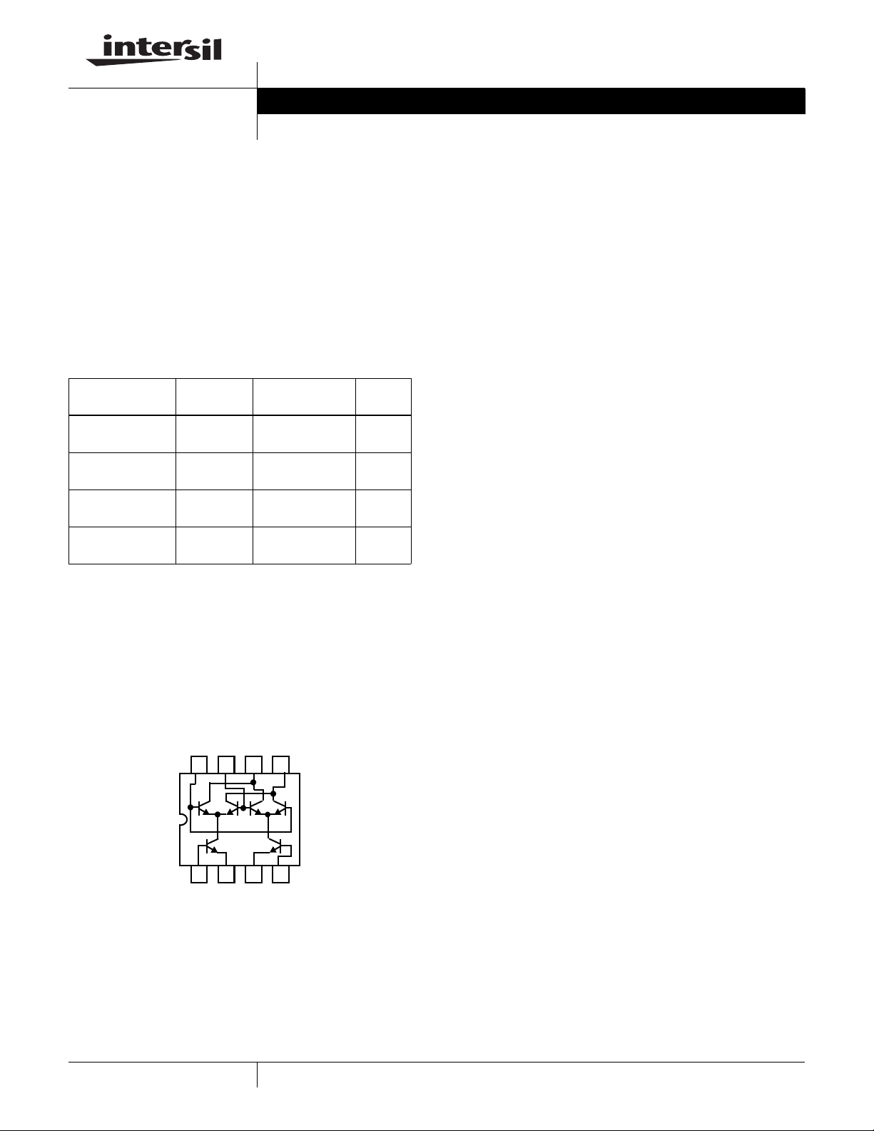
Pinout
HFA3101
(SOIC)
TOP VIEW
8
7
6
5
Q1Q2Q3Q
Q
5
1
2
NOTE: Q5 and Q6 - 2 Paralleled 3µm x 50µm Transistors
Q
, Q2, Q3, Q4 - Single 3µm x 50µm Transistors
1
4
Q
6
3
4
1
CAUTION: These devices are sensitive to electrostatic discharge; follow proper IC Handling Procedures.
1-888-INTERSIL or 321-724-7143
| Intersil (and design) is a registered trademark of Intersil Americas Inc.
Copyright © Intersil Americas Inc. 1998, 2004. All Rights Reserved
All other trademarks mentioned are the property of their respective owners.
Page 2
HFA3101
Absolute Maximum Ratings Thermal Information
V
, Collector to Emitter Voltage . . . . . . . . . . . . . . . . . . . . . . 8.0V
CEO
V
, Collector to Base Voltage. . . . . . . . . . . . . . . . . . . . . . . 12.0V
CBO
V
, Emitter to Base Voltage . . . . . . . . . . . . . . . . . . . . . . . . . 5.5V
EBO
IC, Collector Current . . . . . . . . . . . . . . . . . . . . . . . . . . . . . . . . 30mA
Operating Conditions
Temperature Range. . . . . . . . . . . . . . . . . . . . . . . . . . -40oC to 85oC
CAUTION: Stresses above those listed in “Absolute Maximum Ratings” may cause permanent damage to the device. This is a stress only rating and operation of the
device at these or any other conditions above those indicated in the operational sections of this specification is not implied.
NOTE:
1. θJA is measured with the component mounted on an evaluation PC board in free air.
Thermal Resistance (Typical, Note 1) θJA (oC/W)
SOIC Package . . . . . . . . . . . . . . . . . . . . . . . . . . . . . 185
Maximum Junction Temperature (Die). . . . . . . . . . . . . . . . . . .175oC
Maximum Junction Temperature (Plastic Package). . . . . . . . .150oC
Maximum Storage Temperature Range. . . . . . . . . . -65oC to 150oC
Maximum Lead Temperature (Soldering 10s) . . . . . . . . . . . . .300oC
(SOIC - Lead Tips Only)
Electrical Specifications T
= 25oC
A
(NOTE 2)
TEST
PARAMETER TEST CONDITIONS
Collector to Base Breakdown V oltage, V
Collector to Emitter Breakdown Voltage, V
Q5 and Q
Emitter to Base Breakdown Voltage, V
Collector Cutoff Current, I
Emitter Cutoff Current, I
DC Current Gain, hFE, Q1 thru Q
Collector to Base Capacitance, C
6
(BR)EBO
, Q1 thru Q
CBO
, Q5 and Q
EBO
6
6
CB
, Q1 thru Q6IC = 100µA, IE = 0 A 12 18 - V
(BR)CBO
,
(BR)CEO
, Q1 thru Q6IE = 10µA, IC = 0 A 5.5 6 - V
4
Q1 thru Q
Q5 and Q
Emitter to Base Capacitance, C
EB
Q1 thru Q
Q5 and Q
Current Gain-Bandwidth Product, f
T
Q1 thru Q
Q5 and Q
Power Gain-Bandwidth Product, f
MAX
Q1 thru Q
Q5 and Q
Available Gain at Minimum Noise Figure, G
Q5 and Q
Minimum Noise Figure, NF
50Ω Noise Figure, NF
DC Current Gain Matching, h
Q3 and Q4, and Q5 and Q
6
, Q5 and Q
MIN
, Q5 and Q
50Ω
6
FE1/hFE2
6
, Q1 and Q2,
NFMIN
6
,
Input Offset Voltage, VOS, (Q1 and Q2), (Q3 and Q4),
IC = 100µA, IB = 0 A 8 12 - V
VCB = 8V, IE = 0 A - 0.1 10 nA
VEB = 1V, IC = 0 A - - 200 nA
IC = 10mA, VCE = 3V A 40 70 VCB = 5V, f = 1MHz C - 0.300 - pF
4
6
VEB = 0, f = 1MHz B - 0.200 - pF
4
6
= 10mA, VCE = 5V C - 10 - GHz
4IC
= 20mA, VCE = 5V C - 10 - GHz
6IC
= 10mA, VCE = 5V C - 5 - GHz
4IC
= 20mA, VCE = 5V C - 5 - GHz
6IC
IC = 5mA,
V
= 3V
CE
IC = 5mA,
V
= 3V
CE
IC = 5mA,
V
= 3V
CE
f = 0.5GHz C - 17.5 - dB
f = 1.0GHz C - 11.9 - dB
f = 0.5GHz C - 1.7 - dB
f = 1.0GHz C - 2.0 - dB
f = 0.5GHz C - 2.25 - dB
f = 1.0GHz C - 2.5 - dB
IC = 10mA, VCE = 3V A 0.9 1.0 1.1
IC = 10mA, VCE = 3V A - 1.5 5 mV
LEVEL
MIN TYP MAX UNITS
- 0.600 - pF
- 0.400 - pF
(Q5 and Q6)
Input Offset Current, IC, (Q1 and Q2), (Q3 and Q4),
IC = 10mA, VCE = 3V A - 5 25 µA
(Q5 and Q6)
Input Offset Voltage TC, dVOS/dT, (Q1 and Q2, Q3 and Q4,
Q
and Q6)
5
Collector to Collector Leakage, I
TRENCH-LEAKAGE
IC = 10mA, VCE = 3V C - 0.5 - µV/oC
∆V
= 5V B - 0.01 - nA
TEST
NOTE:
2. Test Level: A. Production Tested, B. Typical or Guaranteed Limit Based on Characterization, C. Design Typical for Information Only.
2
Page 3
HFA3101
PSPICE Model for a 3 µm x 50 µm Transistor
.Model NUHFARRY NPN
+ (IS = 1.840E-16 XTI = 3.000E+00 EG = 1.110E+00 VAF = 7.200E+01
+ VAR = 4.500E+00 BF = 1.036E+02 ISE = 1.686E-19 NE = 1.400E+00
+ IKF = 5.400E-02 XTB = 0.000E+00 BR = 1.000E+01 ISC = 1.605E-14
+ NC = 1.800E+00 IKR = 5.400E-02 RC = 1.140E+01 CJC = 3.980E-13
+ MJC = 2.400E-01 VJC = 9.700E-01 FC = 5.000E-01 CJE = 2.400E-13
+ MJE = 5.100E-01 VJE = 8.690E-01 TR = 4.000E-09 TF = 10.51E-12
+ ITF = 3.500E-02 XTF = 2.300E+00 VTF = 3.500E+00 PTF = 0.000E+00
+ XCJC = 9.000E-01 CJS = 1.689E-13 VJS = 9.982E-01 MJS = 0.000E+00
+ RE = 1.848E+00 RB = 5.007E+01 RBM = 1.974E+00 KF = 0.000E+00
+ AF = 1.000E+00)
Common Emitter S-Parameters of 3 µm x 50 µm Transistor
FREQ. (Hz) |S11| PHASE(S11) |S12| PHASE(S12) |S21| PHASE(S21) |S22| PHASE(S22)
VCE = 5V and IC = 5mA
1.0E+08 0.83 -11.78 1.41E-02 78.88 11.07 168.57 0.97 -11.05
2.0E+08 0.79 -22.82 2.69E-02 68.63 10.51 157.89 0.93 -21.35
3.0E+08 0.73 -32.64 3.75E-02 59.58 9.75 148.44 0.86 -30.44
4.0E+08 0.67 -41.08 4.57E-02 51.90 8.91 140.36 0.79 -38.16
5.0E+08 0.61 -48.23 5.19E-02 45.50 8.10 133.56 0.73 -44.59
6.0E+08 0.55 -54.27 5.65E-02 40.21 7.35 127.88 0.67 -49.93
7.0E+08 0.50 -59.41 6.00E-02 35.82 6.69 123.10 0.62 -54.37
8.0E+08 0.46 -63.81 6.27E-02 32.15 6.11 119.04 0.57 -58.10
9.0E+08 0.42 -67.63 6.47E-02 29.07 5.61 115.57 0.53 -61.25
1.0E+09 0.39 -70.98 6.63E-02 26.45 5.17 112.55 0.50 -63.96
1.1E+09 0.36 -73.95 6.75E-02 24.19 4.79 109.91 0.47 -66.31
1.2E+09 0.34 -76.62 6.85E-02 22.24 4.45 107.57 0.45 -68.37
1.3E+09 0.32 -79.04 6.93E-02 20.53 4.15 105.47 0.43 -70.19
1.4E+09 0.30 -81.25 7.00E-02 19.02 3.89 103.57 0.41 -71.83
1.5E+09 0.28 -83.28 7.05E-02 17.69 3.66 101.84 0.40 -73.31
1.6E+09 0.27 -85.17 7.10E-02 16.49 3.45 100.26 0.39 -74.66
1.7E+09 0.25 -86.92 7.13E-02 15.41 3.27 98.79 0.38 -75.90
1.8E+09 0.24 -88.57 7.17E-02 14.43 3.10 97.43 0.37 -77.05
1.9E+09 0.23 -90.12 7.19E-02 13.54 2.94 96.15 0.36 -78.12
2.0E+09 0.22 -91.59 7.21E-02 12.73 2.80 94.95 0.35 -79.13
2.1E+09 0.21 -92.98 7.23E-02 11.98 2.68 93.81 0.35 -80.09
2.2E+09 0.20 -94.30 7.25E-02 11.29 2.56 92.73 0.34 -80.99
2.3E+09 0.20 -95.57 7.27E-02 10.64 2.45 91.70 0.34 -81.85
2.4E+09 0.19 -96.78 7.28E-02 10.05 2.35 90.72 0.33 -82.68
2.5E+09 0.18 -97.93 7.29E-02 9.49 2.26 89.78 0.33 -83.47
2.6E+09 0.18 -99.05 7.30E-02 8.96 2.18 88.87 0.33 -84.23
2.7E+09 0.17 -100.12 7.31E-02 8.47 2.10 88.00 0.33 -84.97
3-3
Page 4

HFA3101
Common Emitter S-Parameters of 3 µm x 50 µm Transistor (Continued)
FREQ. (Hz) |S
2.8E+09 0.17 -101.15 7.31E-02 8.01 2.02 87.15 0.33 -85.68
2.9E+09 0.16 -102.15 7.32E-02 7.57 1.96 86.33 0.33 -86.37
3.0E+09 0.16 -103.11 7.32E-02 7.16 1.89 85.54 0.33 -87.05
VCE = 5V and IC = 10mA
1.0E+08 0.72 -16.43 1.27E-02 75.41 15.12 165.22 0.95 -14.26
2.0E+08 0.67 -31.26 2.34E-02 62.89 13.90 152.04 0.88 -26.95
3.0E+08 0.60 -43.76 3.13E-02 52.58 12.39 141.18 0.79 -37.31
4.0E+08 0.53 -54.00 3.68E-02 44.50 10.92 132.57 0.70 -45.45
5.0E+08 0.47 -62.38 4.05E-02 38.23 9.62 125.78 0.63 -51.77
6.0E+08 0.42 -69.35 4.31E-02 33.34 8.53 120.37 0.57 -56.72
7.0E+08 0.37 -75.26 4.49E-02 29.47 7.62 116.00 0.51 -60.65
8.0E+08 0.34 -80.36 4.63E-02 26.37 6.86 112.39 0.47 -63.85
9.0E+08 0.31 -84.84 4.72E-02 23.84 6.22 109.36 0.44 -66.49
1.0E+09 0.29 -88.83 4.80E-02 21.75 5.69 106.77 0.41 -68.71
1.1E+09 0.27 -92.44 4.86E-02 20.00 5.23 104.51 0.39 -70.62
1.2E+09 0.25 -95.73 4.90E-02 18.52 4.83 102.53 0.37 -72.28
1.3E+09 0.24 -98.75 4.94E-02 17.25 4.49 100.75 0.35 -73.76
1.4E+09 0.22 -101.55 4.97E-02 16.15 4.19 99.16 0.34 -75.08
1.5E+09 0.21 -104.15 4.99E-02 15.19 3.93 97.70 0.33 -76.28
1.6E+09 0.20 -106.57 5.01E-02 14.34 3.70 96.36 0.32 -77.38
1.7E+09 0.20 -108.85 5.03E-02 13.60 3.49 95.12 0.31 -78.41
1.8E+09 0.19 -110.98 5.05E-02 12.94 3.30 93.96 0.31 -79.37
1.9E+09 0.18 -113.00 5.06E-02 12.34 3.13 92.87 0.30 -80.27
2.0E+09 0.18 -114.90 5.07E-02 11.81 2.98 91.85 0.30 -81.13
2.1E+09 0.17 -116.69 5.08E-02 11.33 2.84 90.87 0.30 -81.95
2.2E+09 0.17 -118.39 5.09E-02 10.89 2.72 89.94 0.29 -82.74
2.3E+09 0.16 -120.01 5.10E-02 10.50 2.60 89.06 0.29 -83.50
2.4E+09 0.16 -121.54 5.11E-02 10.13 2.49 88.21 0.29 -84.24
2.5E+09 0.16 -122.99 5.12E-02 9.80 2.39 87.39 0.29 -84.95
2.6E+09 0.15 -124.37 5.12E-02 9.49 2.30 86.60 0.29 -85.64
2.7E+09 0.15 -125.69 5.13E-02 9.21 2.22 85.83 0.29 -86.32
2.8E+09 0.15 -126.94 5.13E-02 8.95 2.14 85.09 0.29 -86.98
2.9E+09 0.15 -128.14 5.14E-02 8.71 2.06 84.36 0.29 -87.62
3.0E+09 0.14 -129.27 5.15E-02 8.49 1.99 83.66 0.29 -88.25
| PHASE(S11)|S12| PHASE(S12)|S21| PHASE(S21)|S22|PHASE(S22)
11
4
Page 5

HFA3101
Application Information
The HFA3101 array is a very versatile RF Building block. It
has been carefully laid out to improve its matching
properties, bringing the distortion due to area mismatches,
thermal distribution, betas and ohmic resistances to a
minimum.
The cell is equivalent to two differential stages built as two
“variable transconductance multipliers” in parallel, with their
outputs cross coupled. This configuration is well known in
the industry as a Gilbert Cell which enables a four quadrant
multiplication operation.
Due to the input dynamic range restrictions for the input
levels at the upper quad transistors and lower tail transistors,
the HFA3101 cell has restricted use as a linear four quadrant
multiplier. However , its configuration is well suited for uses
where its linear response is limited to one of the inputs only,
as in modulators or mixer circuit applications. Examples of
these circuits are up converters, down converters, frequency
doublers and frequency/phase detectors.
Although linearization is still an issue for the lower pair input,
emitter degeneration can be used to improve the dynamic
range and consequent linearity. The HFA3101 has the lower
pair emitters brought to external pins for this purpose.
Figure 1 shows the typical input waveforms where the
frequency of the carrier is higher than the modulating signal.
The output waveform shows a typical suppressed carrier
output of an up converter or an AM signal generator.
Carrier suppression capability is a property of the well known
Balanced modulator in which the output must be zero when
one or the other input (carrier or modulating signal) is equal
to zero. however, at very high frequencies, high frequency
mismatches and AC offsets are always present and the
suppression capability is often degraded causing carrier and
modulating feedthrough to be present.
Being a frequency translation circuit, the balanced modulator
has the properties of translating the modulating frequency
(ω
) to the carrier frequency (ωC), generating the two side
M
bands ω
some translating schemes being used by
= ωC + ωM and ω
U
ω
- ω
C
M
= ω
- ωM. Figure 2 shows
L
C
balanced mixers.
ω
C
ω
C
+ ω
M
In modulators applications, the upper quad transistors are
used in a switching mode where the pairs Q
and Q3/Q4
1/Q2
act as non saturating high speed switches. These switches
are controlled by the signal often referred as the carrier
input. The signal driving the lower pair Q
is commonly
5/Q6
used as the modulating input. This signal can be linearly
transferred to the output by either the use of low signal lev els
(Well below the thermal voltage of 26mV) or by the use of
emitter degeneration. The chopped waveform appearing at
the output of the upper pair (Q
to Q4) resembles a signal
1
that is multiplied by +1 or -1 at every half cycle of the
switching waveform.
+1
-1
CARRIER SIGNAL
MODULATING SIGNAL
DIFFERENTIAL OUTPUT
FIGURE 2A. UP CONVERSION OR SUPPRESSED CARRIER AM
IF (ωC - ωM)
FOLDED BACK
ω
FIGURE 2B. DOWN CONVERSION
BASEBAND
ω
M
C
ω
C
ω
M
FIGURE 1. TYPICAL MODULATOR SIGNALS
3-5
FIGURE 2C. ZERO IF OR DIRECT DOWN CONVERSION
FIGURE 2. MODULATOR FREQUENCY SPECTRUM
Page 6

HFA3101
The use of the HFA3101 as modulators has several
advantages when compared to its counterpart, the dio de
doublebalanced mixer, in which it is required to receive
enough energy to drive the diodes into a switching mode and
has also some requirements depending on the frequency
range desired, of different transformers to suit specific
frequency responses. The HFA3101 requires very low
driving capabilities for its carrier input and its frequency
response is limited by the f
of the devices, the design and
T
the layout techniques being utilized.
Up conversion uses, for UHF transmitters for e xample , can be
performed by injecting a
modulating input in the range of
45MHz to 130MHz that carries the information often called IF
(Intermediate frequency) for up conversion (The IF signal has
been previously modulated by some modulation scheme from a
baseband signal of audio or digital information) and by injecting
the signal of a local oscillator of a much higher frequency range
from 600MHz to 1.2GHz into the carrier input. Using the
example of a 850MHz carrier input and a 70MHz IF, the output
spectrum will contain a upper side band of 920MHz, a lower
side band of 780MHz and some of the carrier (850MHz) and IF
(70MHz) feedthrough. A Band pass filter at the output can
attenuate the undesirable signals and the 920MHz signal can
be routed to a transmitter RF power amplifier .
Down conversion, as the name implies, is the process used
to translate a higher frequency signal to a lower frequency
range conserving the modulation information contai ned in
the higher frequency signal. One very common typical down
conversion use for example, is for superheterodyne radio
receivers where a translated lower frequency often referred
as intermediate frequency (IF) is used for detection or
demodulation of the baseband signal. Other application uses
include down conversion f or special filtering using frequency
translation methods.
An oscillator referred as the local oscillator (LO) drives the
upper quad transistors of the cell with a frequency called
ω
. The lower pair is driven by the RF signal of frequency
C
ω
to be translated to a lower frequency IF . The spectrum of
M
the IF output will contain the sum and difference of the
frequencies
ω
and ωM. Notice that the difference can
C
become negative when the frequency of the local oscillator is
lower than the incoming frequency and the signal is folded
back as in Figure 2.
NOTE: The acronyms R F , IF and LO are often interchanged in the
industry depending on the application of the cell as mixers or
modulators. The output of the cell also contains multiples of the
frequency of the signal being fed to the upper quad pair of transistors
because of the switching action equivalent to a square wave
multiplication. In practice, however, not only the odd multiples in the
case of a symmetrical square wave but some of the even multiples
will also appear at the output spectrum due to the nature of the actual
switching wav eform and high frequency performance. By-products of
the form M*
integers are also expected to be present at the output and their lev els
are carefully examined and minimized by the design. This distortion
is considered one of the figures of merit for a mixer application.
ω
+ N*ωM with M and N being positive or negative
C
The process of frequency doubling is also understood by
having the same signal being fed to both modulating and
carrier ports. The output frequency will be the sum of
and
ω
which is equivalent to the product of the input
M
ω
C
frequency by 2 and a zero Hz or DC frequency equivalent to
the difference of
ω
and ωM . Figure 2 also shows one
C
technique in use today where a process of down conversion
named zero IF is made by using a local oscillator with a very
pure signal frequency equal to the incoming RF frequency
signal that contains a baseband (audio or digital signal)
modulation. Although complex, the extraction or detection of
the signal is straightforward.
Another useful application of the HFA3101 is its use as a high
frequency phase detector where the two signals are fed to the
carrier and modulation ports and the DC inf ormation is
extracted from its output. In this case, both ports are utilized in a
switching mode or overdrive, such that the process of
multiplication tak es plac e in a quasi di gital f orm (2 square
waves). One application of a phase detector is frequency or
phase demodulation where the FM signal is split before the
modulating and carrier ports. The lo wer input port is always 90
degrees apart from the carrier input signal through a high Q
tuned phase shift network. The network, being tuned for a
precise 90 degrees shift at a nominal frequency, will set the two
signals 90 degrees apart and a quiescent output DC level will
be present at the output. When the input signal is frequency
modulated, the phase shift of the signal coming from the
network will deviate from 90 degrees proportional to the
frequency deviation of the FM signal and a DC variation at the
output will take place, resembling the demodulated FM signal.
The HFA3101 could also be used for quadrature detection,
(I/Q demodulation), AGC control with limited range, low le v el
multiplication to name a few other applications.
Biasing
Various biasing schemes can be employed f or use with the
HFA3101. Figure 3 shows the most common schemes. The
biasing method is a choice of the designer when cost,
thermal dependence, voltage overheads and DC balancing
properties are taken into consideration.
Figure 3A shows the simplest form of biasing the HFA3101.
The current source required for the lower pair is set by the
voltage across the resistor R
lower transistor . To increase the overhead, collector resistors
are substituted by an RF choke as the upper pair functions
as a current source for AC signals. The bases of the upper
and lower transistors are biased by R
respectively. The voltage drop across the resistor R
be higher than a V
with an increase sufficient to assure
BE
that the collector to base junctions of the lower pair are
always reverse biased. Notice that this same voltage also
sets the V
of operation of the lower pair which is important
CE
for the optimization of gain. Resistors R
zero for applications where the input signals are well below
25mV peak. Resistors R
EE
less a VBE drop of the
BIAS
and RB2
B1
are nominally
EE
must
2
are used to increase the linea rity
6
Page 7

HFA3101
of the circuit upon higher level signals. The drop across REE
must be taken into consideration when setting the current
source value.
Figure 3B depicts the use of a common resistor sharing the
current through the cell which is used for temperature
V
CC
L
R
R
BIAS
R
B1
R
1
8
7
Q1Q2Q3Q
Q
2
5
1
2
R
EE
R
B2
CH
6
5
4
Q
6
3
4
R
EE
R
E
R
R
BIAS
2
R
R
1
8
Q1Q2Q3Q
1
R
R
compensation as the lower pair V
o
-2mV/
C.
drop at the rate of
BE
Figure 3C uses a split supply.
V
R
R
1
8
Q1Q2Q3Q
1
CC
L
B1
7
Q
5
2
R
EE
R
B2
R
CH
6
5
4
Q
6
3
4
R
EE
E
R
C
V
CC
L
B1
7
Q
5
2
EE
B2
CH
6
5
R
R
2
BIAS
4
Q
6
3
4
R
EE
R
E
FIGURE 3A.
Design Example: Down Converter Mixer
Figure 4 shows an example of a low cost mixer for cellular
applications.
LO IN
0.01
0.01
0.01
0.01
825MHz
V
CC
110
330
220
51
8
Q1Q2Q3Q
1
7
Q
5
2
FIGURE 4. 3V DOWN CONVERTER APPLICATION
L
CH
390nH
6
5
4
Q
6
3
4
27
2K
5p TO 12p
51
0.01
V
CC
0.1
IF OUT
75MHz
RF IN
900MHz
FIGURE 3B.
FIGURE 3.
3V
V
EE
FIGURE 3C.
The design flexibility of the HFA3101 is demonstrated by a
low cost, and low voltage mixer application at the 900MHz
range. The choice of good quality chip components with their
self resonance outside the boundaries of the application are
important. The design has been optimized to accommodate
the evaluation of the same layout for various quiescent
current values and lower supply voltages. The choice of R
E
became important for the available overhead and also for
maintaining an AC true impedance for high frequency
signals. The value of 27Ω has been found to be the optimum
minimum for the application. The input impedances of the
HFA3101 base input ports are high eno ugh to permit their
termination with 50Ω resistors. Notice the AC termination by
decoupling the bias circuit through good quality capacitors.
The choice of the bias has been related to the available
power supply voltage with the values of R
splitting the voltages for optimum V
CE
, R2 and R
1
BIAS
values. For e v aluation
of the cell quiescent currents, the voltage at the emitter
resistor R
has been recorded.
E
The gain of the circuit, being a function of the load and the
combined emitter resistances at high frequencies have been
kept to a maximum by the use of an output match network.
The high output impedance of the HFA3101 permits
3-7
Page 8

HFA3101
broadband match if so desired at 50Ω (RL = 50Ω to 2kΩ) as
well as with tuned medium Q matching networks (L, T etc.).
Stability
The cell, by its nature, has very high gain and precautions
must be taken to account for the combination of signal
reflections, gain, layout and package parasitics. The rule of
thumb of avoiding reflected waves must be observed. It is
important to assure good matching between the mixer stage
and its front end. Laboratory measurements have shown
some susceptibility for oscillation at the upper quad
transistors input. Any LO prefiltering has to be designed
such the return loss is maintained within acceptable limits
specially at high frequencies. Typical off the shelf fil ters
exhibits very poor return loss for signals outside the
passband. It is suggested that a “pad” or a broadband
resistive network be used to interface the LO port with a
filter. The inclusion of a parallel 2K resistor in the load
decreases the gain slightly which improves the stability
factor and also improves the distortion products (output
intermodulation or 3rd order intercept). The employment of
good RF techniques shall suffice the stability requirements.
Evaluation
The evaluation of the HFA3101 in a mixer configuration is
presented in Figures 6 to 11, Tab le 1 and Table 2. The layout
is depicted in Figure 5.
setup as in Table 1. S
characterization is enough to assure
22
the calculation of L, T or transmission line matching
networks.
TABLE 1. S22 P ARAMETERS FOR DO WN CONVERSION,
= 10µH
L
CH
FREQUENCY RESISTANCE REACTANCE
10MHz 265Ω 615Ω
45MHz 420Ω - 735Ω
75MHz 122Ω - 432Ω
100MHz 67Ω - 320Ω
TABLE 2. TYPICAL PARAMETERS FOR DOWN
PARAMETER LO LEVEL
Power Gain -6dBm 8.5dB
TOI Output -6dBm 11.5dBm
NF SSB -6dBm 14.5dB
Power Gain 0dBm 8.6dB
TOI Output 0dBm 11dBm
NF SSB 0dBm 15dB
PARAMETER LO LEVEL
Power Gain -6dBm 10dB
TOI Output -6dBm 13dBm
NF SSB -6dBm 20dB
Power Gain 0dBm 11dB
TOI Output 0dBm 12.5dBm
NF SSB 0dBm 24dB
CONVERSION, L
= 10µH
CH
VCC = 3V,
I
= 8mA
BIAS
VCC = 4V,
I
= 19mA
BIAS
FIGURE 5. UP/DOWN CONVERTER LAYOUT , 400%;
MATERIAL G10, 0.031
The output matching network has been designed from data
taken at the output port at various test frequencies with the
8
TABLE 3. TYPICAL VALUES OF S22 FOR THE OUTPUT PORT .
= 390nH I
L
CH
FREQUENCY RESISTANCE REACTANCE
300MHz 22Ω -115Ω
600MHz 7.5Ω -43Ω
900MHz 5.2Ω -14Ω
1.1GHz 3.9Ω 0Ω
TABLE 4. TYPICAL VALUES OF S22. LCH = 390nH, I
FREQUENCY RESISTANCE REACTANCE
300MHz 23.5Ω -110Ω
600MHz 10.3Ω -39Ω
900MHz 8.7Ω -14Ω
1.1GHz 8Ω 0Ω
= 8mA (SET UP OF FIGURE 11)
BIAS
BIAS
= 18mA
Page 9

HFA3101
Up Converter Example
An application for a up converter as well as a frequency
multiplier can be demonstrated using the same layout, with
an addition of matching components. The output port S
must be characterized for proper matching procedures and
depending on the frequency desired for the output,
transmission line transformations can be designed. The
return loss of the input ports maintain acceptable values in
VCC 3V
L
CH
8
7
6
5
Q1Q2Q3Q
Q
5
1
2
4
Q
6
3
4
FIGURE 6. OUTPUT PORT S22 TEST SET UP
0.1
2K
22
excess of 1.2GHz which can permit the evaluation of a
frequency doubler to 2.4GHz if so desired.
The addition of the resistors REE can increase considerably
the dynamic range of the up converter as demonstrated at
Figure 13. The evaluation results depicted in Table 5 have
been obtained by a triple stub tuner as a matching network
for the output due to the layout constraints. Based on the
evaluation results it is clear that the cell requires a higher
Bias current for overall performance.
S
LOG MAG
0dB
5dB/DIV
4V
3V
100MHz
FIGURE 7. LO PORT RETURN LOSS
11
1.1GHz
LOG MAG
S
0dB
10dB/DIV
100MHz 1.1GHz
11
FIGURE 8. RF PORT RETURN LOSS
RF = 901MHz - 25dBm
LO = 825MHz -6dBm
10dB/
DIV
64M
11*LO - 10RF
76MHz
-17dBm
12RF - 13LOIF
88M
SPAN
40MHz
FIGURE 10. TYPICAL IN BAND OUTPUT SPECTRUM, VCC = 3V
LOG MAG
S
0dB
5dB/DIV
10MHz
22
110MHz
FIGURE 9. IF PORT RETURN LOSS, WITH MATCHING
NETWORK
RF = 900MHz -25dBm
LO = 825MHz -6dBm
10dB/
DIV
-53dBm
675 750 825 900 975
LO - 2RF
-26dBm
-36dBm
-58dBm
LO + 2RF
SPAN
500MHz
FIGURE 11. TYPICAL OUT OF BAND OUTPUT SPECTRUM
3-9
Page 10

HFA3101
Design Example: Up Converter Mixer
Figure 12 shows an example of an up converter for cellular
applications.
Conclusion
The HFA3101 offers the designer a number of choices and
different applications as a powerful RF building block.
Although isolation is degraded from the theoretical results for
the cell due to the unbalanced, nondifferential input schemes
being used, a number of advantages can be taken into
consideration like cost, flexibility, low power and small outline
when deciding for a design.
47-100pF
51
8
Q1Q2Q3Q
1
825MHz
0.01
0.01
LO IN
V
CC
0.01
3V
110
330
TABLE 5. TYPICAL PARAMETERS FOR THE UP
CONVERTER EXAMPLE
PARAMETER
VCC = 3V,
I
= 8mA
BIAS
VCC = 4V,
I
= 18mA
BIAS
Power Gain, LO = -6dBm 3dB 5.5dBm
Power Gain, LO = 0dBm 4dB 7.2dB
RF Isolation, LO = 0dBm 15dBc 22dBc
LO Isolation, LO = 0dBm 28dBc 28dBc
VCC 3V
0.1
390nH
0.01
5.2nH
7
6
5
4
Q
Q
5
6
2
3
4
11p
0.01
900MHz
RF IN
75MHz
0.01
OUTPUT WITHOUT EMITTER DEGENERATION
901 912890
2LO - 10RF 12RF
RF = 76MHz
LO = 825MHz
FIGURE 13. TYPICAL SPECTRUM PERFORMANCE OF UP CONVERTER
51
220
R
EE
R
EE
27
FIGURE 12. UP CONVERTER
OUTPUT WITH EMITTER DEGENERATION REE = 4.7Ω
SPAN
50MHz
EXP ANDE D SPECTR UM REE = 4.7Ω
825 900 976
10
Page 11

HFA3101
Typical Performance Curves for Transistors
70
60
50
40
(mA)
C
I
30
20
10
0
02.0 6.04.0
IB = 1mA
IB = 800µA
IB = 600µA
IB = 400µA
IB = 200µA
FIGURE 14. IC vs V
0
10
VCE = 3V
-2
10
-4
10
(A)
B
-6
10
AND I
C
I
-8
10
VCE (V)
CE
140
VCE = 5V
120
100
80
FE
h
60
40
20
0
-10
10
12
10
8
6
(GHz)
T
f
4
-8
10
-6
10
IC (A)
FIGURE 15. HFE vs I
-4
10
-2
10
0
10
C
-10
10
-12
10
0.20 0.40 0.60 0.80 1.0
VBE (V)
FIGURE 16. GUMMEL PLOT FIGURE 17. fT vs I
4.8
4.6
4.4
4.2
4.0
3.8
NOISE FIGURE (dB)
3.6
3.4
3.2
FIGURE 18. GAIN AND NOISE FIGURE vs FREQUENCY
NOTE: Figures 14 through 18 are only for Q5 and Q6.
2
0
-4
10
-3
10
IC (A)
-2
10
C
20
18
16
14
| (dB)
12
21
|S
10
8
6
0.5 1.51.0 2.002.53.0
FREQUENCY (GHz)
4
-1
10
3-11
Page 12

Die Characteristics
HFA3101
PROCESS
UHF-1
DIE DIMENSIONS:
53 mils x 52 mils x 14 mils
1340µm x 1320µm x 355.6µm
METALLIZATION:
Type: Metal 1: AlCu(2%)/TiW
Thickness: Metal 1: 8kÅ ±0.5kÅ
Type: Metal 2: AlCu(2%)
Thickness: Metal 2: 16kÅ ±0.8kÅ
Metallization Mask Layout
PASSIVATION:
Type: Nitride
Thickness: 4kÅ ±0.5kÅ
SUBSTRATE POTENTIAL (Powered Up):
Floating
HFA3101
77
8
6
6
5
8
1
1
2233
5
4
4
All Intersil semiconductor products are manufactured, assembled and tested under ISO9000 quality systems certification.
Intersil semiconductor products are sold by de scription only. Intersil Corporation reserves the right to make changes in circuit design and/or specifications at any time without
notice. Accordingly, the reader is cautioned to verify that data sheets are current before placing orders. Information furnished by Intersil is believed to be accurate and reliable. However, no respon sibi lity i s assu med by Intersil or its subsidiaries for its use; nor for any infringements of patents or other rights of third parties which may result from
its use. No license is granted by implication or otherwise under any patent or patent rights of Intersil or its subsidiaries.
For information regarding Intersil Corporation and its products, see web site www.intersil.com
12
 Loading...