

®
HFA3046, HFA3096, HFA3127, HFA3128
Data Sheet
Ultra High Frequency Transistor Arrays
The HFA3046, HFA3096, HFA3127 and the HFA3128 are
Ultra High Frequency Transistor Arrays that are fabricated
from Intersil Corporation’s complementary bipolar UHF-1
process. Each array consists of five dielectrically isolated
transistors on a common monolithic substrate. The NPN
transistors exhibit a f
provide a f
of 5.5GHz. Both types exhibit low noise (3.5dB),
T
making them ideal for high frequency amplifier and mixer
applications.
The HFA3046 and HFA3127 are all NPN arrays while the
HFA3128 has all PNP transistors. The HFA3096 is an
NPN-PNP combination. Access is provided to each of the
terminals for the individual transistors for maximum
application flexibility. Monolithic construction of these
transistor arrays provides close electrical and thermal
matching of the five transistors.
Intersil provides an Application Note illustrating the use of
these devices as RF amplifiers. For more information, visit
our website at www.intersil.com.
of 8GHz while the PNP transistors
T
December 21, 2005
FN3076.13
Features
• NPN Transistor (fT) . . . . . . . . . . . . . . . . . . . . . . . . . 8GHz
• NPN Current Gain (h
• NPN Early Voltage (V
• PNP Transistor (f
• PNP Current Gain (h
• PNP Early Voltage (V
). . . . . . . . . . . . . . . . . . . . . . . . 130
FE
) . . . . . . . . . . . . . . . . . . . . . . . 50V
A
). . . . . . . . . . . . . . . . . . . . . . . . . 5.5GHz
T
). . . . . . . . . . . . . . . . . . . . . . . . . 60
FE
) . . . . . . . . . . . . . . . . . . . . . . . .20V
A
• Noise Figure (50Ω) at 1.0GHz . . . . . . . . . . . . . . . . . 3.5dB
• Collector to Collector Leakage. . . . . . . . . . . . . . . . . .<1pA
• Complete Isolation Between Transistors
• Pin Compatible with Industry Standard 3XXX Series
Arrays
• Pb-Free Plus Anneal Available (RoHS Compliant)
Applications
• VHF/UHF Amplifiers
•VHF/UHF Mixers
• IF Converters
• Synchronous Detectors
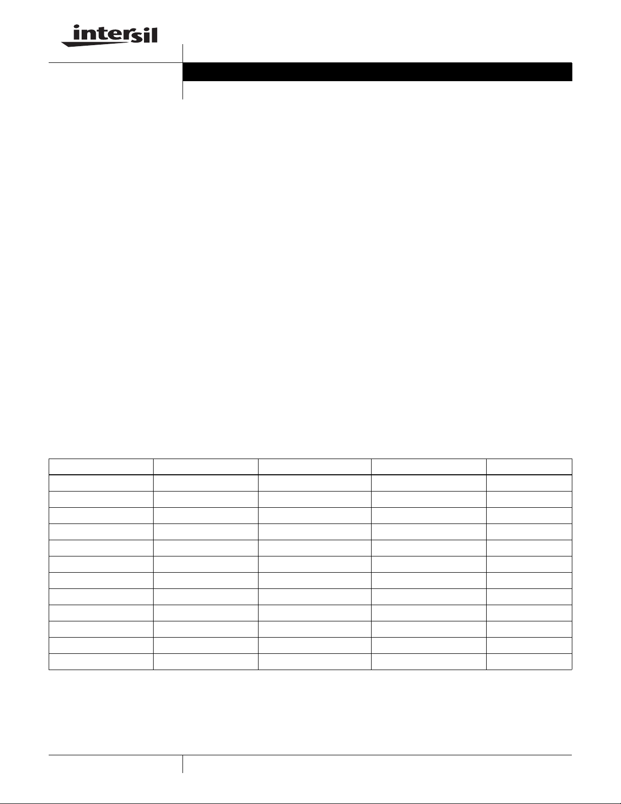
Ordering Information
PART NUMBER* PART MARKING TEMP. RANGE (°C) PACKAGE PKG. DWG. #
HFA3046B HFA3046B -55 to 125 14 Ld SOIC M14.15
HFA3046BZ (Note) HFA3046BZ -55 to 125 14 Ld SOIC (Pb-free) M14.15
HFA3096B HFA3096B -55 to 125 16 Ld SOIC M16.15
HFA3096BZ (Note) HFA3096BZ -55 to 125 16 Ld SOIC (Pb-free) M16.15
HFA3127B HFA3127B -55 to 125 16 Ld SOIC M16.15
HFA3127BZ (Note) HFA3127BZ -55 to 125 16 Ld SOIC (Pb-free) M16.15
HFA3127R 127 -55 to 125 16 Ld 3x3 QFN L16.3x3
HFA3127RZ (Note) 127Z -55 to 125 16 Ld 3x3 QFN (Pb-free) L16.3x3
HFA3128B HFA3128B -55 to 125 16 Ld SOIC M16.15
HFA3128BZ (Note) HFA3128BZ -55 to 125 16 Ld SOIC (Pb-free) M16.15
HFA3128R 128 -55 to 125 16 Ld 3x3 QFN L16.3x3
HFA3128RZ (Note) 128Z -55 to 125 16 Ld 3x3 QFN (Pb-free) L16.3x3
*Add “96” suffix for tape and reel.
NOTE: Intersil Pb-free plus anneal products employ special Pb-free material sets; molding compounds/die attach materials and 100% matte tin plate
termination finish, which are RoHS compliant and compatible with both SnPb and Pb-free soldering operations. Intersil Pb-free products are MSL
classified at Pb-free peak reflow temperatures that meet or exceed the Pb-free requirements of IPC/JEDEC J STD-020.
1
CAUTION: These devices are sensitive to electrostatic discharge; follow proper IC Handling Procedures.
1-888-INTERSIL or 1-888-468-3774
| Intersil (and design) is a registered trademark of Intersil Americas Inc.
Copyright Intersil Americas Inc. 1998, 2005. All Rights Reserved
All other trademarks mentioned are the property of their respective owners.

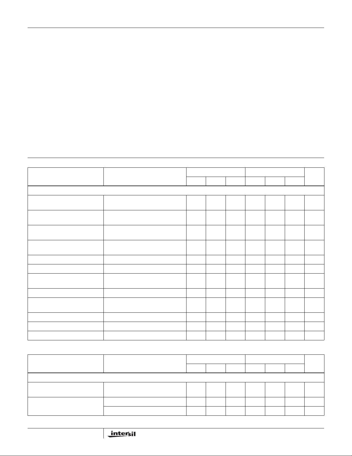
Pinouts
1
Q
2
3
Q
4
5
6
7
HFA3046
TOP VIEW
1
Q
5
2
Q
4
Q
3
HFA3046, HFA3096, HFA3127, HFA3128
HFA3096
TOP VIEW
NC
14
13
12
11
10
9
8
1
Q
1
2
3
4
Q
2
5
6
7
Q
3
8
16
15
Q
5
14
13
12
Q
4
11
10
9
NC
HFA3127, HFA3128
TOP VIEW
Q2C
Q1C
Q1E
15
16 14 13
1
2
3
4
5
6
7
8
Q1B
HFA3127
TOP VIEW
Q
Q
2
Q
3
HFA3128
TOP VIEW
16
1
15
14
Q
5
13
12
11
10
Q
4
9
NC
1
2
3
Q
2
4
5
6
7
Q
3
8
16
Q
1
15
14
Q
5
13
12
11
10
Q
4
9
Q2E
Q2B
NC
Q3C
1
2
3
4
6578
Q3E
Q3B
12
Q5B
11
Q5E
10
Q5C
9
Q4C
Q4B
Q4E
2
FN3076.13
December 21, 2005
HFA3046, HFA3096, HFA3127, HFA3128
Absolute Maximum Ratings Thermal Information
Collector to Emitter Voltage (Open Base) . . . . . . . . . . . . . . . . . . 8V
Collector to Base Voltage (Open Emitter) . . . . . . . . . . . . . . . . . 12V
Emitter to Base Voltage (Reverse Bias). . . . . . . . . . . . . . . . . . . 5.5V
Collector Current (100% Duty Cycle) . . . . . . 18.5mA at T
34mA at T
37mA at T
= 150°C
J
= 125°C
J
= 110°C
J
Peak Collector Current (Any Condition). . . . . . . . . . . . . . . . . . 65mA
Operating Information
Temperature Range . . . . . . . . . . . . . . . . . . . . . . . . . -55°C to 125°C
CAUTION: Stresses above those listed in “Absolute Maximum Ratings” may cause permanent damage to the device. This is a stress only rating and operation of the
device at these or any other conditions above those indicated in the operational sections of this specification is not implied.
NOTES:
is measured with the component mounted on an evaluation PC board in free air.
1. θ
JA
2. For θ
3. θ
, the “case temp” location is the center of the exposed metal pad on the package underside.
JC
is measured with the component mounted on a high effective thermal conductivity test board in free air. See Tech Brief TB379 for details.
JA
Thermal Resistance (Typical) θ
(°C/W) θJC (°C/W)
JA
14 Ld SOIC Package (Note 1) . . . . . . . 120 N/A
16 Ld SOIC Package (Note 1) . . . . . . . 115 N/A
QFN Package (Notes 2, 3). . . . . . . . . . 57 10
Maximum Power Dissipation (Any One Transistor) . . . . . . . . 0.15W
Maximum Junction Temperature (Die) . . . . . . . . . . . . . . . . . . . 175°C
Maximum Junction Temperature (Plastic Package) . . . . . . . 150°C
Maximum Storage Temperature Range . . . . . . . . . . -65°C to 150°C
Maximum Lead Temperature (Soldering 10s) . . . . . . . . . . . . 300°C
(SOIC - Lead Tips Only)
Electrical Specifications T
= 25°C
A
DIE SOIC, QFN
PARAMETER TEST CONDITIONS
UNITSMIN TYP MAX MIN TYP MAX
DC NPN CHARACTERISTICS
Collector to Base Breakdown
Voltage, V
(BR)CBO
Collector to Emitter Breakdown
Voltage, V
(BR)CEO
Collector to Emitter Breakdown
Voltage, V
(BR)CES
Emitter to Base Breakdown
Voltage, V
Collector-Cutoff-Current, I
Collector-Cutoff-Current, I
(BR)EBO
CEO
CBO
Collector to Emitter Saturation
Voltage, V
Base to Emitter Voltage, V
CE(SAT)
BE
DC Forward-Current Transfer
Ratio, h
FE
Early Voltage, V
A
Base to Emitter Voltage Drift I
IC = 100µA, IE = 0 12 18 - 12 18 - V
IC = 100µA, IB = 0 8 12 - 8 12 - V
IC = 100µA, Base Shorted to Emitter 10 20 - 10 20 - V
IE = 10µA, IC = 0 5.5 6 - 5.5 6 - V
VCE = 6V, IB = 0 - 2 100 - 2 100 nA
VCB = 8V, IE = 0 - 0.1 10 - 0.1 10 nA
IC = 10mA, IB = 1mA - 0.3 0.5 - 0.3 0.5 V
IC = 10mA - 0.85 0.95 - 0.85 0.95 V
IC = 10mA, VCE = 2V 40 130 - 40 130 -
IC = 1mA, VCE = 3.5V 20 50 - 20 50 - V
= 10mA - -1.5 - - -1.5 - mV/°C
C
Collector to Collector Leakage - 1 - - 1 - pA
Electrical Specifications T
= 25°C
A
PARAMETER TEST CONDITIONS
DYNAMIC NPN CHARACTERISTICS
Noise Figure f = 1.0GHz, V
I
= 5mA, ZS = 50Ω
C
Current Gain-Bandwidth
f
T
Product
IC = 1mA, VCE = 5V - 5.5 - - 5.5 - GHz
I
= 10mA, VCE = 5V - 8 - - 8 - GHz
C
3
CE
= 5V,
DIE SOIC, QFN
UNITSMIN TYP MAX MIN TYP MAX
- 3.5 - - 3.5 - dB
FN3076.13
December 21, 2005
HFA3046, HFA3096, HFA3127, HFA3128
Electrical Specifications T
= 25°C (Continued)
A
DIE SOIC, QFN
PARAMETER TEST CONDITIONS
Power Gain-Bandwidth Product,
f
MAX
Base to Emitter Capacitance V
Collector to Base Capacitance V
Electrical Specifications T
IC = 10mA, VCE = 5V - 6 - - 2.5 - GHz
= -3V - 200 - - 500 - fF
BE
= 3V - 200 - - 500 - fF
CB
= 25°C
A
UNITSMIN TYP MAX MIN TYP MAX
DIE SOIC, QFN
PARAMETER TEST CONDITIONS
UNITSMIN TYP MAX MIN TYP MAX
DC PNP CHARACTERISTICS
Collector to Base Breakdown
Voltage, V
(BR)CBO
Collector to Emitter Breakdown
Voltage, V
(BR)CEO
Collector to Emitter Breakdown
Voltage, V
(BR)CES
Emitter to Base Breakdown
Voltage, V
Collector Cutoff Current, I
Collector Cutoff Current, I
(BR)EBO
CEO
CBO
Collector to Emitter Saturation
Voltage, V
Base to Emitter Voltage, V
CE(SAT)
BE
DC Forward-Current Transfer
Ratio, h
FE
Early Voltage, V
A
Base to Emitter Voltage Drift I
IC = -100µA, IE = 0 10 15 - 10 15 - V
IC = -100µA, IB = 0 8 15 - 8 15 - V
IC = -100µA, Base Shorted to Emitter 10 15 - 10 15 - V
IE = -10µA, IC = 0 4.5 5 - 4.5 5 - V
VCE = -6V, IB = 0 - 2 100 - 2 100 nA
VCB = -8V, IE = 0 - 0.1 10 - 0.1 10 nA
IC = -10mA, IB = -1mA - 0.3 0.5 - 0.3 0.5 V
IC = -10mA - 0.85 0.95 - 0.85 0.95 V
IC = -10mA, VCE = -2V 20 60 - 20 60 -
IC = -1mA, VCE = -3.5V 10 20 - 10 20 - V
= -10mA - -1.5 - - -1.5 - mV/°C
C
Collector to Collector Leakage - 1 - - 1 - pA
Electrical Specifications T
= 25°C
A
PARAMETER TEST CONDITIONS
DYNAMIC PNP CHARACTERISTICS
Noise Figure f = 1.0GHz, V
I
= -5mA, ZS = 50Ω
C
Current Gain-Bandwidth
f
T
Product
Power Gain-Bandwidth
Product
Base to Emitter Capacitance V
Collector to Base Capacitance V
IC = -1mA, VCE = -5V - 2 - - 2 - GHz
I
= -10mA, VCE = -5V - 5.5 - - 5.5 - GHz
C
I
= -10mA, VCE = -5V - 3 - - 2 - GHz
C
= 3V - 200 - - 500 - fF
BE
= -3V - 300 - - 600 - fF
CB
4
CE
= -5V,
DIE SOIC, QFN
UNITSMIN TYP MAX MIN TYP MAX
- 3.5 - - 3.5 - dB
FN3076.13
December 21, 2005
HFA3046, HFA3096, HFA3127, HFA3128
Electrical Specifications T
PARAMETER TEST CONDITIONS
DIFFERENTIAL PAIR MATCHING CHARACT ERISTICS FOR THE HFA3046
Input Offset Voltage I
Input Offset Current I
Input Offset Voltage TC I
S-Parameter and PSPICE model data is available from Intersil Sales Offices, and Intersil Corporation’s web site.
= 25°C (Continued)
A
DIE SOIC, QFN
= 10mA, VCE = 5V - 1.5 5.0 - 1.5 5.0 mV
C
= 10mA, VCE = 5V - 5 25 - 5 25 µA
C
= 10mA, VCE = 5V - 0.5 - - 0.5 - µV/°C
C
UNITSMIN TYP MAX MIN TYP MAX
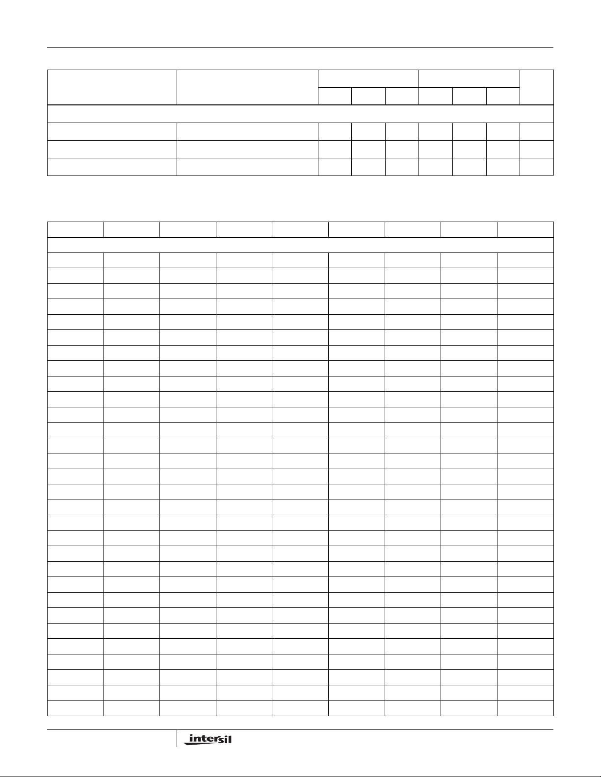
Common Emitter S-Parameters of NPN 3µm x 50 µm Transistor
FREQ. (Hz) |S11| PHASE(S11)|S21| PHASE(S21)|S12| PHASE(S12)|S22|PHASE(S22)
V
= 5V and IC = 5mA
CE
1.0E+08 0.83 -11.78 11.07 168.57 1.41E-02 78.88 0.97 -11.05
2.0E+08 0.79 -22.82 10.51 157.89 2.69E-02 68.63 0.93 -21.35
3.0E+08 0.73 -32.64 9.75 148.44 3.75E-02 59.58 0.86 -30.44
4.0E+08 0.67 -41.08 8.91 140.36 4.57E-02 51.90 0.79 -38.16
5.0E+08 0.61 -48.23 8.10 133.56 5.19E-02 45.50 0.73 -44.59
6.0E+08 0.55 -54.27 7.35 127.88 5.65E-02 40.21 0.67 -49.93
7.0E+08 0.50 -59.41 6.69 123.10 6.00E-02 35.82 0.62 -54.37
8.0E+08 0.46 -63.81 6.11 119.04 6.27E-02 32.15 0.57 -58.10
9.0E+08 0.42 -67.63 5.61 115.57 6.47E-02 29.07 0.53 -61.25
1.0E+09 0.39 -70.98 5.17 112.55 6.63E-02 26.45 0.50 -63.96
1.1E+09 0.36 -73.95 4.79 109.91 6.75E-02 24.19 0.47 -66.31
1.2E+09 0.34 -76.62 4.45 107.57 6.85E-02 22.24 0.45 -68.37
1.3E+09 0.32 -79.04 4.15 105.47 6.93E-02 20.53 0.43 -70.19
1.4E+09 0.30 -81.25 3.89 103.57 7.00E-02 19.02 0.41 -71.83
1.5E+09 0.28 -83.28 3.66 101.84 7.05E-02 17.69 0.40 -73.31
1.6E+09 0.27 -85.17 3.45 100.26 7.10E-02 16.49 0.39 -74.66
1.7E+09 0.25 -86.92 3.27 98.79 7.13E-02 15.41 0.38 -75.90
1.8E+09 0.24 -88.57 3.10 97.43 7.17E-02 14.43 0.37 -77.05
1.9E+09 0.23 -90.12 2.94 96.15 7.19E-02 13.54 0.36 -78.12
2.0E+09 0.22 -91.59 2.80 94.95 7.21E-02 12.73 0.35 -79.13
2.1E+09 0.21 -92.98 2.68 93.81 7.23E-02 11.98 0.35 -80.09
2.2E+09 0.20 -94.30 2.56 92.73 7.25E-02 11.29 0.34 -80.99
2.3E+09 0.20 -95.57 2.45 91.70 7.27E-02 10.64 0.34 -81.85
2.4E+09 0.19 -96.78 2.35 90.72 7.28E-02 10.05 0.33 -82.68
2.5E+09 0.18 -97.93 2.26 89.78 7.29E-02 9.49 0.33 -83.47
2.6E+09 0.18 -99.05 2.18 88.87 7.30E-02 8.96 0.33 -84.23
2.7E+09 0.17 -100.12 2.10 88.00 7.31E-02 8.47 0.33 -84.97
2.8E+09 0.17 -101.15 2.02 87.15 7.31E-02 8.01 0.33 -85.68
2.9E+09 0.16 -102.15 1.96 86.33 7.32E-02 7.57 0.33 -86.37
3.0E+09 0.16 -103.11 1.89 85.54 7.32E-02 7.16 0.33 -87.05
5
FN3076.13
December 21, 2005

HFA3046, HFA3096, HFA3127, HFA3128
Common Emitter S-Parameters of NPN 3µm x 50 µm Transistor (Continued)
FREQ. (Hz) |S
VCE = 5V and IC = 10mA
1.0E+08 0.72 -16.43 15.12 165.22 1.27E-02 75.41 0.95 -14.26
2.0E+08 0.67 -31.26 13.90 152.04 2.34E-02 62.89 0.88 -26.95
3.0E+08 0.60 -43.76 12.39 141.18 3.13E-02 52.58 0.79 -37.31
4.0E+08 0.53 -54.00 10.92 132.57 3.68E-02 44.50 0.70 -45.45
5.0E+08 0.47 -62.38 9.62 125.78 4.05E-02 38.23 0.63 -51.77
6.0E+08 0.42 -69.35 8.53 120.37 4.31E-02 33.34 0.57 -56.72
7.0E+08 0.37 -75.26 7.62 116.00 4.49E-02 29.47 0.51 -60.65
8.0E+08 0.34 -80.36 6.86 112.39 4.63E-02 26.37 0.47 -63.85
9.0E+08 0.31 -84.84 6.22 109.36 4.72E-02 23.84 0.44 -66.49
1.0E+09 0.29 -88.83 5.69 106.77 4.80E-02 21.75 0.41 -68.71
1.1E+09 0.27 -92.44 5.23 104.51 4.86E-02 20.00 0.39 -70.62
1.2E+09 0.25 -95.73 4.83 102.53 4.90E-02 18.52 0.37 -72.28
1.3E+09 0.24 -98.75 4.49 100.75 4.94E-02 17.25 0.35 -73.76
1.4E+09 0.22 -101.55 4.19 99.16 4.97E-02 16.15 0.34 -75.08
1.5E+09 0.21 -104.15 3.93 97.70 4.99E-02 15.19 0.33 -76.28
1.6E+09 0.20 -106.57 3.70 96.36 5.01E-02 14.34 0.32 -77.38
1.7E+09 0.20 -108.85 3.49 95.12 5.03E-02 13.60 0.31 -78.41
1.8E+09 0.19 -110.98 3.30 93.96 5.05E-02 12.94 0.31 -79.37
1.9E+09 0.18 -113.00 3.13 92.87 5.06E-02 12.34 0.30 -80.27
2.0E+09 0.18 -114.90 2.98 91.85 5.07E-02 11.81 0.30 -81.13
2.1E+09 0.17 -116.69 2.84 90.87 5.08E-02 11.33 0.30 -81.95
2.2E+09 0.17 -118.39 2.72 89.94 5.09E-02 10.89 0.29 -82.74
2.3E+09 0.16 -120.01 2.60 89.06 5.10E-02 10.50 0.29 -83.50
2.4E+09 0.16 -121.54 2.49 88.21 5.11E-02 10.13 0.29 -84.24
2.5E+09 0.16 -122.99 2.39 87.39 5.12E-02 9.80 0.29 -84.95
2.6E+09 0.15 -124.37 2.30 86.60 5.12E-02 9.49 0.29 -85.64
2.7E+09 0.15 -125.69 2.22 85.83 5.13E-02 9.21 0.29 -86.32
2.8E+09 0.15 -126.94 2.14 85.09 5.13E-02 8.95 0.29 -86.98
2.9E+09 0.15 -128.14 2.06 84.36 5.14E-02 8.71 0.29 -87.62
3.0E+09 0.14 -129.27 1.99 83.66 5.15E-02 8.49 0.29 -88.25
| PHASE(S11)|S21| PHASE(S21)|S12| PHASE(S12)|S22|PHASE(S22)
11
Common Emitter S-Parameters of PNP 3µm x 50 µm Transistor
FREQ. (Hz) |S11| PHASE(S11)|S21| PHASE(S21)|S12| PHASE(S12)|S22|PHASE(S22)
= -5V and IC = -5mA
V
CE
1.0E+08 0.72 -16.65 10.11 166.77 1.66E-02 77.18 0.96 -10.76
2.0E+08 0.68 -32.12 9.44 154.69 3.10E-02 65.94 0.90 -20.38
3.0E+08 0.62 -45.73 8.57 144.40 4.23E-02 56.39 0.82 -28.25
4.0E+08 0.57 -57.39 7.68 135.95 5.05E-02 48.66 0.74 -34.31
5.0E+08 0.52 -67.32 6.86 129.11 5.64E-02 42.52 0.67 -38.81
6
FN3076.13
December 21, 2005

HFA3046, HFA3096, HFA3127, HFA3128
Common Emitter S-Parameters of PNP 3µm x 50 µm Transistor (Continued)
FREQ. (Hz) |S
6.0E+08 0.47 -75.83 6.14 123.55 6.07E-02 37.66 0.61 -42.10
7.0E+08 0.43 -83.18 5.53 118.98 6.37E-02 33.79 0.55 -44.47
8.0E+08 0.40 -89.60 5.01 115.17 6.60E-02 30.67 0.51 -46.15
9.0E+08 0.38 -95.26 4.56 111.94 6.77E-02 28.14 0.47 -47.33
1.0E+09 0.36 -100.29 4.18 109.17 6.91E-02 26.06 0.44 -48.15
1.1E+09 0.34 -104.80 3.86 106.76 7.01E-02 24.33 0.41 -48.69
1.2E+09 0.33 -108.86 3.58 104.63 7.09E-02 22.89 0.39 -49.05
1.3E+09 0.32 -112.53 3.33 102.72 7.16E-02 21.67 0.37 -49.26
1.4E+09 0.30 -115.86 3.12 101.01 7.22E-02 20.64 0.36 -49.38
1.5E+09 0.30 -118.90 2.92 99.44 7.27E-02 19.76 0.34 -49.43
1.6E+09 0.29 -121.69 2.75 98.01 7.32E-02 19.00 0.33 -49.44
1.7E+09 0.28 -124.24 2.60 96.68 7.35E-02 18.35 0.32 -49.43
1.8E+09 0.28 -126.59 2.47 95.44 7.39E-02 17.79 0.31 -49.40
1.9E+09 0.27 -128.76 2.34 94.29 7.42E-02 17.30 0.30 -49.38
2.0E+09 0.27 -130.77 2.23 93.19 7.45E-02 16.88 0.30 -49.36
2.1E+09 0.26 -132.63 2.13 92.16 7.47E-02 16.52 0.29 -49.35
2.2E+09 0.26 -134.35 2.04 91.18 7.50E-02 16.20 0.28 -49.35
2.3E+09 0.26 -135.96 1.95 90.24 7.52E-02 15.92 0.28 -49.38
2.4E+09 0.25 -137.46 1.87 89.34 7.55E-02 15.68 0.28 -49.42
2.5E+09 0.25 -138.86 1.80 88.48 7.57E-02 15.48 0.27 -49.49
2.6E+09 0.25 -140.17 1.73 87.65 7.59E-02 15.30 0.27 -49.56
2.7E+09 0.25 -141.39 1.67 86.85 7.61E-02 15.15 0.26 -49.67
2.8E+09 0.25 -142.54 1.61 86.07 7.63E-02 15.01 0.26 -49.81
2.9E+09 0.24 -143.62 1.56 85.31 7.65E-02 14.90 0.26 -49.96
3.0E+09 0.24 -144.64 1.51 84.58 7.67E-02 14.81 0.26 -50.13
= -5V, IC = -10mA
V
CE
1.0E+08 0.58 -23.24 13.03 163.45 1.43E-02 73.38 0.93 -13.46
2.0E+08 0.53 -44.07 11.75 149.11 2.58E-02 60.43 0.85 -24.76
3.0E+08 0.48 -61.50 10.25 137.78 3.38E-02 50.16 0.74 -33.10
4.0E+08 0.43 -75.73 8.88 129.12 3.90E-02 42.49 0.65 -38.83
5.0E+08 0.40 -87.36 7.72 122.49 4.25E-02 36.81 0.58 -42.63
6.0E+08 0.37 -96.94 6.78 117.33 4.48E-02 32.59 0.51 -45.07
7.0E+08 0.35 -104.92 6.01 113.22 4.64E-02 29.39 0.47 -46.60
8.0E+08 0.33 -111.64 5.39 109.85 4.76E-02 26.94 0.43 -47.49
9.0E+08 0.32 -117.36 4.87 107.05 4.85E-02 25.04 0.40 -47.97
1.0E+09 0.31 -122.27 4.44 104.66 4.92E-02 23.55 0.37 -48.18
1.1E+09 0.30 -126.51 4.07 102.59 4.97E-02 22.37 0.35 -48.20
1.2E+09 0.30 -130.21 3.76 100.76 5.02E-02 21.44 0.33 -48.11
| PHASE(S11)|S21| PHASE(S21)|S12| PHASE(S12)|S22|PHASE(S22)
11
7
FN3076.13
December 21, 2005
Common Emitter S-Parameters of PNP 3µm x 50 µm Transistor (Continued)
FREQ. (Hz) |S
| PHASE(S11)|S21| PHASE(S21)|S12| PHASE(S12)|S22|PHASE(S22)
11
1.3E+09 0.29 -133.46 3.49 99.14 5.06E-02 20.70 0.32 -47.95
1.4E+09 0.29 -136.33 3.25 97.67 5.09E-02 20.11 0.31 -47.77
1.5E+09 0.28 -138.89 3.05 96.33 5.12E-02 19.65 0.30 -47.58
1.6E+09 0.28 -141.17 2.87 95.10 5.15E-02 19.29 0.29 -47.39
1.7E+09 0.28 -143.21 2.70 93.96 5.18E-02 19.01 0.28 -47.23
1.8E+09 0.28 -145.06 2.56 92.90 5.21E-02 18.80 0.27 -47.09
1.9E+09 0.27 -146.73 2.43 91.90 5.23E-02 18.65 0.27 -46.98
2.0E+09 0.27 -148.26 2.31 90.95 5.26E-02 18.55 0.26 -46.91
2.1E+09 0.27 -149.65 2.20 90.05 5.28E-02 18.49 0.26 -46.87
2.2E+09 0.27 -150.92 2.10 89.20 5.30E-02 18.46 0.25 -46.87
2.3E+09 0.27 -152.10 2.01 88.37 5.33E-02 18.47 0.25 -46.90
2.4E+09 0.27 -153.18 1.93 87.59 5.35E-02 18.50 0.25 -46.97
2.5E+09 0.27 -154.17 1.86 86.82 5.38E-02 18.55 0.24 -47.07
2.6E+09 0.26 -155.10 1.79 86.09 5.40E-02 18.62 0.24 -47.18
2.7E+09 0.26 -155.96 1.72 85.38 5.42E-02 18.71 0.24 -47.34
2.8E+09 0.26 -156.76 1.66 84.68 5.45E-02 18.80 0.24 -47.55
2.9E+09 0.26 -157.51 1.60 84.01 5.47E-02 18.91 0.24 -47.76
3.0E+09 0.26 -158.21 1.55 83.35 5.50E-02 19.03 0.23 -48.00
Typical Performance Curves
I
25
20
15
10
COLLECTOR CURRENT (mA)
5
0
12345
COLLECTOR TO EMITTER VOLTAGE (V)
FIGURE 1. NPN COLLECTOR CURRENT vs COLLECTOR TO
EMITTER VOLTAGE
= 200µA
B
I
= 160µA
B
I
=120µA
B
I
= 80µA
B
I
= 40µA
B
FIGURE 2. NPN COLLECTOR CURRENT AND BASE
CURRENT vs BASE TO EMITTER VOLTAGE
8
FN3076.13
December 21, 2005

Typical Performance Curves (Continued)
GAIN BANDWIDTH PRODUCT (GHz)
10.0
8.0
6.0
4.0
2.0
VCE = 5V
VCE = 1V
0
0.1
1.0 10 100
COLLECTOR CURRENT (mA)
VCE = 3V
160
140
120
100
DC CURRENT GAIN
80
60
40
20
0
VCE = 3V
1µ
10µ 100µ 1m 10m 100m
COLLECTOR CURRENT (A)
FIGURE 3. NPN DC CURRENT GAIN vs COLLECTOR CURRENT FIGURE 4. NPN G AI N BANDWIDT H PRODUCT vs C OL LE C T O R
CURRENT (UHF 3 x 50 WITH BOND P A DS)
-25
-20
-15
-10
-5
COLLECTOR CURRENT (mA)
I
= -400µA
B
I
= -320µA
B
I
= -240µA
B
I
= -160µA
B
I
= -80µA
B
0
0
-1 -2 -3 -4 -5
COLLECTOR TO EMITTER VOLTAGE (V)
FIGURE 5. PNP COLLECTOR CURRENT vs COLLECTOR TO
EMITTER VOLTAGE
FIGURE 7. PNP DC CURRENT GAIN vs COLLECTOR
CURRENT
FIGURE 6. PNP COLLECTOR CURRENT AND BASE
CURRENT vs BASE TO EMITTER VOLTAGE
FIGU RE 8. P NP GAIN BANDWIDTH PRODUCT vs COLLECTOR
CURRENT (UHF 3 x 50 WITH BOND P A DS)
9
FN3076.13
December 21, 2005

Die Characteristics
HFA3046, HFA3096, HFA3127, HFA3128
DIE DIMENSIONS:
53 mils x 52 mils x 19 mils
1340µm x 1320µm x 483µm
METALLIZATION:
Type: Metal 1: AlCu(2%)/TiW
Thickness: Metal 1: 8kÅ ±0.4kÅ
Type: Metal 2: AlCu(2%)
Thickness: Metal 2: 16k
Å ±0.8kÅ
Metallization Mask Layout
1340µm
(53 mils)
PAS S I VATI O N:
Type: Nitride
Thickness: 4kÅ ±0.5kÅ
PROCESS:
UHF-1
SUBSTRATE POTENTIAL: (POWERED UP)
Unbiased
HFA3096, HFA3127, HFA3128
12
3
4
5
6
78 910
1516
14
13
12
11
1320µm
(52 mils)
HFA3046
1340µm
(53 mils)
3
4
5
6
12
78
1320µm
(52 mils)
1314
9
Pad numbers correspond to SOIC pinout.
12
11
10
10
FN3076.13
December 21, 2005

HFA3046, HFA3096, HFA3127, HFA3128
Small Outline Plastic Packages (SOIC)
N
INDEX
AREA
123
-A-
E
-B-
SEATING PLANE
D
A
-C-
0.25(0.010) BM M
H
L
h x 45
o
α
e
B
0.25(0.010) C AM BS
M
NOTES:
1. Symbols are defined in the “MO Series Symbol List” in Section 2.2 of
Publication Number 95.
2. Dimensioning and tolerancing per ANSI Y14.5M-1982.
3. Dimension “D” does not include mold flash, protrusions or gate burrs.
Mold flash, protrusion and gate burrs shall not exceed 0.15mm (0.006
inch) per side.
4. Dimension “E” does not include interlead flash or protrusions. Interlead
flash and protrusions shall not exceed 0.25mm (0.010 inch) per side.
5. The chamfer on the body is optional. If it is not present, a visual index
feature must be located within the crosshatched area.
6. “L” is the length of terminal for soldering to a substrate.
7. “N” is the number of terminal positions.
8. Terminal numbers are shown for reference only.
9. The lead width “B”, as measured 0.36mm (0.014 inch) or greater
above the seating plane, shall not exceed a maximum value of
0.61mm (0.024 inch).
10. Controlling dimension: MILLIMETER. Converted inch dimensions
are not necessarily exact.
A1
C
0.10(0.004)
M14.15 (JEDEC MS-012-AB ISSUE C)
14 LEAD NARROW BODY SMALL OUTLINE PLASTIC
PACKAGE
INCHES MILLIMETERS
SYMBOL
A 0.0532 0.0688 1.35 1.75 -
A1 0.0040 0.0098 0.10 0.25 -
B 0.013 0.020 0.33 0.51 9
C 0.0075 0.0098 0.19 0.25 -
D 0.3367 0.3444 8.55 8.75 3
E 0.1497 0.1574 3.80 4.00 4
e 0.050 BSC 1.27 BSC -
H 0.2284 0.2440 5.80 6.20 -
h 0.0099 0.0196 0.25 0.50 5
L 0.016 0.050 0.40 1.27 6
N14 147
α
0° 8° 0° 8° -
NOTESMIN MAX MIN MAX
Rev. 0 12/93
11
FN3076.13
December 21, 2005

HFA3046, HFA3096, HFA3127, HFA3128
Small Outline Plastic Packages (SOIC)
N
INDEX
AREA
E
-B-
H
0.25(0.010) BM
123
SEATING PLANE
-A-
D
e
B
0.25(0.010) C AM BS
M
A
-C-
A1
0.10(0.004)
L
h x 45°
C
NOTES:
1. Symbols are defined in the “MO Series Symbol List” in Section 2.2 of
Publication Number 95.
2. Dimensioning and tolerancing per ANSI Y14.5M-1982.
3. Dimension “D” does not include mold flash, protrusions or gate burrs.
Mold flash, protrusion and gate burrs shall not exceed 0.15mm (0.006
inch) per side.
4. Dimension “E” does not include interlead flash or protrusions. Interlead
flash and protrusions shall not exceed 0.25mm (0.010 inch) per side.
5. The chamfer on the body is optional. If it is not present, a visual index
feature must be located within the crosshatched area.
6. “L” is the length of terminal for soldering to a substrate.
7. “N” is the number of terminal positions.
8. Terminal numbers are shown for reference only.
9. The lead width “B”, as measured 0.36mm (0.014 inch) or greater above
the seating plane, shall not exceed a maximum value of 0.61mm
(0.024 inch).
10. Controlling dimension: MILLIMETER. Converted inch dimensions are
not necessarily exact.
12
FN3076.13
December 21, 2005

HFA3046, HFA3096, HFA3127, HFA3128
Quad Flat No-Lead Plastic Package (QFN)
Micro Lead Frame Plastic Package (MLFP)
2X
0.15
A
E1/2 E/2
A2
A1
A3
8
E2
E2/2
9
CORNER
OPTION 4X
A1
C
E1
A
7
8
9
/ /
0.10 C
0.08
9
(Ne-1)Xe
REF.
C
L
E
B
e
0.152XB
C
L1
C
L
10
A
6
INDEX
AREA
AREA
2X
2X
SEATING PLANE
(DATUM B)
(DATUM A)
INDEX
AREA
FOR ODD TERMINAL/SIDE FOR EVEN TERMINAL/SIDE
0.15
6
4X
CC
C
C
4X P
4X P
NX L
e
1
2
3
B
AC0.15
0
8
C
L
D
9
N
BOTTOM VIEW
D1
D1/2
N
TOP VIEW
SIDE VIEW
NX b
D2
D2
2
e
(Nd-1)Xe
REF.
NX b
5
SECTION "C-C"
L1
TERMINAL TIP
D/2
5
0.10 BAMC
7
NX k
N
1
2
3
L
10
L16.3x3
16 LEAD QUAD FLAT NO-LEAD PLASTIC PA CKAGE
MILLIMETERS
SYMBOL
A 0.80 0.90 1.00 -
A1 - - 0.05 -
A2 - - 1.00 9
A3 0.20 REF 9
b 0.18 0.23 0.30 5, 8
D 3.00 BSC -
D1 2.75 BSC 9
D2 1.35 1.50 1.65 7, 8, 10
E 3.00 BSC -
E1 2.75 BSC 9
E2 1.35 1.50 1.65 7, 8, 10
e 0.50 BSC -
k0.20 - - -
L 0.30 0.40 0.50 8
N162
Nd 4 3
Ne 4 3
P- -0.609
θ --129
NOTES:
1. Dimensioning and tolerancing conform to ASME Y14.5-1994.
2. N is the number of terminals.
3. Nd and Ne refer to the number of terminals on each D and E.
4. All dimensions are in millimeters. Angles are in degrees.
5. Dimension b applies to the metallized terminal and is measured
between 0.15mm and 0.30mm from the terminal tip.
6. The configuration of the pin #1 identifier is optional, but must be
located within the zone indicated. The pin #1 identifier may be
either a mold or mark feature.
7. Dimensions D2 and E2 are for the exposed pads which provide
improved electrical and thermal performance.
8. Nominal dimensions are provided to assist with PCB Land
Pattern Design efforts, see Intersil Technical Brief TB389.
9. Features and dimensions A2, A3, D1, E1, P & θ are present when
Anvil singulation method is used and not present for saw
singulation.
10. Compliant to JEDEC MO-220VEED-2 Issue C, except for the E2
and D2 MAX dimension.
NOTESMIN NOMINAL MAX
Rev. 1 6/04
All Intersil U.S. products are manufactured, assembled and tested utilizing ISO9000 quality systems.
Intersil Corporation’s quality certifications can be viewed at www.intersil.com/design/quality
Intersil products are sold by description only. Intersil Corporation reserves the right to make changes in circuit design, software and/or specifications at any time without
notice. Accordingly, the reader is cautioned to verify that data sheets are current before placing orders. Information furnished by Intersil is believed to be accurate and
reliable. However, no responsibility is assumed by Intersil or its subsidiaries for its use; nor for any infringements of patents or other rights of third parties which may result
from its use. No license is granted by implication or otherwise under any patent or patent rights of Intersil or its subsidiaries.
For information regarding Intersil Corporation and its products, see www.intersil.com
13
FN3076.13
December 21, 2005
 Loading...