Intersil Corporation HFA1305 Datasheet

HFA1305
Data Sheet April 1999
Triple, 560MHz, Low Power, Video
Operational Amplifier
The HFA1305 is a triple, high speed, low power current
feedback amplifier built with Intersil’s proprietary
complementary bipolar UHF-1 process.
These amplifiers deliver up to 560MHz bandwidth and
1700V/µs slew rate,ononly58mWofquiescentpower.They
are specifically designed to meet the performance, power,
and cost requirements of high volume video applications.
The excellent gain flatness and differential gain/phase
performance make these amplifiers well suited for
component or composite video applications. Video
performance is maintained even when driving a double
terminated cable (R
when driving two double terminated cables (R
= 150Ω), and degrades only slightly
L
=75Ω). RGB
L
applications will benefit from the high slew rates, and high
full power bandwidth.
The HFA1305 is a pin compatible, low power, high
performance upgrade for the popular Intersil HA5013, and
for the AD8073 and CLC5623, in ±5V applications.
Ordering Information
TEMP.
PART NUMBER
HFA1305IB -40 to 85 14 Ld SOIC M14.15
HA5025EVAL High Speed Op Amp DIP Evaluation Board
RANGE (oC) PACKAGE
PKG.
NO.
File Number 4727
Features
• Low Supply Current . . . . . . . . . . . . . . . . . 5.8mA/Op Amp
• High Input Impedance . . . . . . . . . . . . . . . . . . . . . . . 1MΩ
• Wide -3dB Bandwidth (A
= +2). . . . . . . . . . . . . . 560MHz
V
• Very Fast Slew Rate. . . . . . . . . . . . . . . . . . . . . . 1700V/µs
• Gain Flatness (to 50MHz). . . . . . . . . . . . . . . . . . . . ±0.03dB
• Differential Gain . . . . . . . . . . . . . . . . . . . . . . . . . . . 0.02%
• Differential Phase. . . . . . . . . . . . . . . . . . . . 0.03 Degrees
• All Hostile Crosstalk (5MHz). . . . . . . . . . . . . . . . . . -60dB
• Pin Compatible Upgrade to HA5013, AD8073 and
CLC5623 in ±5V Supply Applications
Applications
• Flash A/D Drivers
• Professional Video Processing
• Video Digitizing Boards/Systems
• Computer Video Plug-In Boards
• RGB Preamps
• Medical Imaging
• Hand Held and Miniaturized RF Equipment
• Battery Powered Communications
• High Speed Oscilloscopes and Analyzers
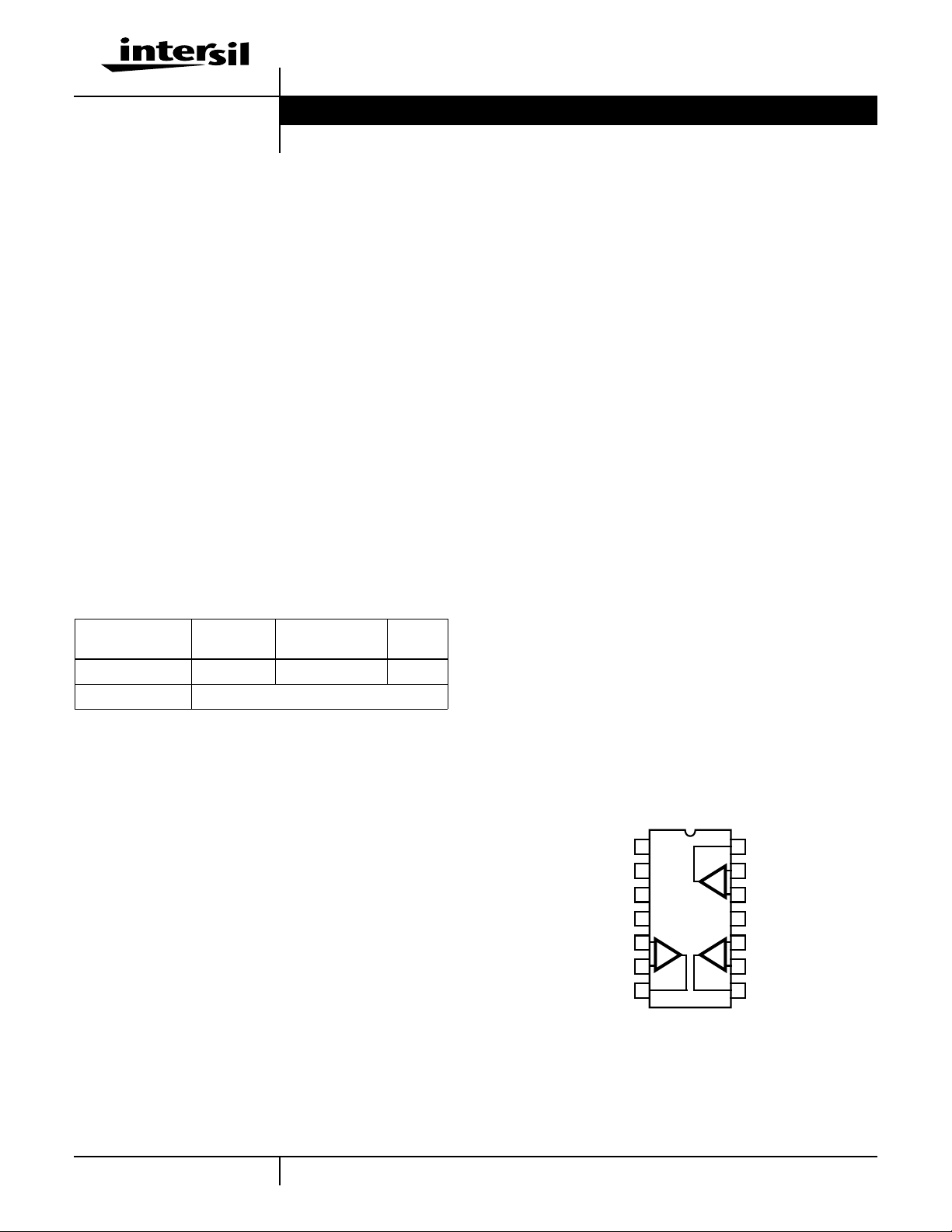
Pinout
HFA1305
(SOIC)
TOP VIEW
NC
1
2
NC
3
NC
4
V+
5
+IN 1
-IN 1
OUT 1
1
CAUTION: These devices are sensitive to electrostatic discharge; follow proper IC Handling Procedures.
1-888-INTERSIL or 321-724-7143
+
-
6
7
| Copyright © Intersil Corporation 1999
14
OUT 3
13
-IN 3
-
+
12
+IN 3
11
V-
10
+IN 2
+
-
9
-IN 2
8
OUT 2

HFA1305
Absolute Maximum Ratings T
Voltage Between V+ and V-. . . . . . . . . . . . . . . . . . . . . . . . . . . . 11V
DC Input Voltage . . . . . . . . . . . . . . . . . . . . . . . . . . . . . . . . V
Differential Input Voltage . . . . . . . . . . . . . . . . . . . . . . . . . . . . . . . 5V
Output Current (Note 2). . . . . . . . . . . . . . . . .Short Circuit Protected
ESD Rating
Human Body Model (Per MIL-STD-883 Method 3015.7). . . 600V
= 25oC Thermal Information
A
Thermal Resistance (Typical, Note 1) θJA (oC/W)
SUPPLY
30mA Continuous
60mA ≤ 50% Duty Cycle
SOIC Package . . . . . . . . . . . . . . . . . . . . . . . . . . . . . 120
Maximum Junction Temperature (Plastic Package) . . . . . . . 150oC
Maximum Storage Temperature Range. . . . . . . . . . -65oC to 150oC
Maximum Lead Temperature (Soldering 10s) . . . . . . . . . . . . 300oC
(Lead Tips Only)
Operating Conditions
Temperature Range. . . . . . . . . . . . . . . . . . . . . . . . . . -40oC to 85oC
CAUTION: Stresses above those listed in “Absolute Maximum Ratings” may cause permanent damage to the device. This is a stress only rating and operation of the
device at these or any other conditions above those indicated in the operational sections of this specification is not implied.
NOTES:
1. θJA is measured with the component mounted on an evaluation PC board in free air.
2. Output is short circuitprotected to ground.Briefshort circuits togroundwill not degradereliability, however continuous(100%duty cycle) output
current must not exceed 30mA for maximum reliability.
Electrical Specifications V
PARAMETER TEST CONDITIONS
INPUT CHARACTERISTICS
Input Offset Voltage A 25 - 2 5 mV
Average Input Offset Voltage Drift B Full - 1 10 µV/oC
Input Offset Voltage
Common-Mode Rejection Ratio
Input Offset Voltage
Power Supply Rejection Ratio
Non-Inverting Input Bias Current A 25 - 6 15 µA
Non-Inverting Input Bias Current Drift B Full - 5 60 nA/oC
Non-Inverting Input Bias Current
Power Supply Sensitivity
Non-Inverting Input Resistance ∆VCM = ±1.8V A 25 0.8 1.2 - MΩ
Inverting Input Bias Current A 25 - 2 7.5 µA
Inverting Input Bias Current Drift B Full - 60 200 nA/oC
Inverting Input Bias Current
Common-Mode Sensitivity
= ±5V, AV = +1, RF = 510Ω, RL = 100Ω, Unless Otherwise Specified
SUPPLY
(NOTE 4)
TESTLEVEL
A Full - 3 8 mV
∆VCM = ±1.8V A 25 45 48 - dB
∆VCM = ±1.8V A 85 43 46 - dB
∆VCM = ±1.2V A -40 43 46 - dB
∆VPS = ±1.8V A 25 48 52 - dB
∆VPS = ±1.8V A 85 46 48 - dB
∆VPS = ±1.2V A -40 46 48 - dB
A Full - 10 25 µA
∆VPS = ±1.8V A 25 - 0.5 1 µA/V
∆VPS = ±1.8V A 85 - 0.8 3 µA/V
∆VPS = ±1.2V A -40 - 0.8 3 µA/V
∆VCM = ±1.8V A 85 0.5 0.8 - MΩ
∆VCM = ±1.2V A -40 0.5 0.8 - MΩ
A Full - 5 15 µA
∆VCM = ±1.8V A 25 - 3 6 µA/V
∆VCM = ±1.8V A 85 - 4 8 µA/V
∆VCM = ±1.2V A -40 - 4 8 µA/V
TEMP.
(oC)
HFA1305IB (SOIC)
UNITSMIN TYP MAX
2

HFA1305
Electrical Specifications V
PARAMETER TEST CONDITIONS
Inverting Input Bias Current Power Supply
Sensitivity
Inverting Input Resistance C 25 - 60 - Ω
Input Capacitance B 25 - 1.4 - pF
Input Voltage Common Mode Range
(Implied by VIO CMRR, +RIN, and -I
CMS Tests)
Input Noise Voltage Density f = 100kHz B 25 - 3.5 - nV/√Hz
Non-Inverting Input Noise Current Density f = 100kHz B 25 - 2.5 - pA/√Hz
Inverting Input Noise Current Density f = 100kHz B 25 - 20 - pA/√Hz
TRANSFER CHARACTERISTICS
Open Loop Transimpedance Gain C 25 - 500 - kΩ
AC CHARACTERISTICS (Note 3)
-3dB Bandwidth
(V
= 0.2V
OUT
Full Power Bandwidth
(V
= 5V
OUT
Gain Flatness
(V
= 0.2V
OUT
Minimum Stable Gain A Full - 1 - V/V
Crosstalk
(AV = +2, All Channels Hostile, Note 5)
OUTPUT CHARACTERISTICS AV = +2 (Note 3), Unless Otherwise Specified
Output Voltage Swing
(Note 5)
Output Current
(Note 5)
Output Short Circuit Current B 25 - 90 - mA
Closed Loop Output Impedance B 25 - 0.2 - Ω
, Notes 3, 5)
P-P
, Notes 3, 5)
P-P
, Notes 3, 5)
P-P
= ±5V, AV = +1, RF = 510Ω, RL = 100Ω, Unless Otherwise Specified (Continued)
SUPPLY
HFA1305IB (SOIC)
BIAS
(NOTE 4)
TESTLEVEL
∆VPS = ±1.8V A 25 - 2 5 µA/V
∆VPS = ±1.8V A 85 - 4 8 µA/V
∆VPS = ±1.2V A -40 - 4 8 µA/V
A 25, 85 ±1.8 ±2.4 - V
A -40 ±1.2 ±1.7 - V
AV = +1 B 25 - 375 - MHz
AV = -1 B 25 - 420 - MHz
AV = +2 B 25 - 560 - MHz
AV = +1 B 25 - 160 - MHz
AV = -1 B 25 - 260 - MHz
AV = +2 B 25 - 165 - MHz
AV = +1, To 25MHz B 25 - ±0.03 - dB
AV = +1, To 50MHz B 25 - ±0.03 - dB
AV = +1, To 100MHz B 25 - ±0.07 - dB
AV = -1, To 25MHz B 25 - ±0.03 - dB
AV = -1, To 50MHz B 25 - ±0.04 - dB
AV = +2, To 25MHz B 25 - ±0.03 - dB
AV = +2, To 50MHz B 25 - ±0.03 - dB
AV = +2, To 100MHz B 25 - ±0.07 - dB
5MHz B 25 - -60 - dB
10MHz B 25 - -56 - dB
AV = -1, RL = 100Ω A25±3 ±3.4 - V
A Full ±2.8 ±3- V
AV = -1, RL = 50Ω A 25, 85 50 60 - mA
A -40 28 42 - mA
TEMP.
(oC)
UNITSMIN TYP MAX
3

HFA1305
Electrical Specifications V
PARAMETER TEST CONDITIONS
Second Harmonic Distortion
(V
= 2V
OUT
Third Harmonic Distortion
(V
= 2V
OUT
P-P
P-P
, Note 5)
, Note 5)
= ±5V, AV = +1, RF = 510Ω, RL = 100Ω, Unless Otherwise Specified (Continued)
SUPPLY
(NOTE 4)
TESTLEVEL
TEMP.
(oC)
HFA1305IB (SOIC)
10MHz B 25 - -51 - dBc
20MHz B 25 - -46 - dBc
10MHz B 25 - -63 - dBc
20MHz B 25 - -56 - dBc
UNITSMIN TYP MAX
TRANSIENT CHARACTERISTICS AV = +2 (Note 3), Unless Otherwise Specified
Rise and Fall Times
(V
OUT
= 0.5V
P-P
, Note 3)
Overshoot
(V
OUT
= 0.5V
P-P
, VIN t
Notes 3, 6)
RISE
= 1ns,
AV = +1 B 25 - 1.0 - ns
AV = +2 B 25 - 0.8 - ns
AV = +1, +OS B 25 - 5 - %
AV = +1, -OS B 25 - 11 - %
AV = -1, +OS B 25 - 7 - %
AV = -1, -OS B 25 - 8 - %
AV = +2, +OS B 25 - 5 - %
AV = +2, -OS B 25 - 10 - %
Slew Rate
(V
= 5V
OUT
V
= 4V
OUT
Notes 3, 5)
at AV = +2, -1,
P-P
, at AV = +1,
P-P
AV = +1, +SR B 25 - 1230 - V/µs
AV = +1, -SR B 25 - 1350 - V/µs
AV = -1, +SR B 25 - 2500 - V/µs
AV = -1, -SR B 25 - 1900 - V/µs
AV = +2, +SR B 25 - 1700 - V/µs
AV = +2, -SR B 25 - 1700 - V/µs
Settling Time
(V
= +2V to 0V Step, Note 5)
OUT
To 0.1% B 25 - 23 - ns
To 0.05% B 25 - 30 - ns
To 0.025% B 25 - 37 - ns
Overdrive Recovery Time VIN = ±2V B 25 - 8.5 - ns
VIDEO CHARACTERISTICS AV = +2 (Note 3), Unless Otherwise Specified
Differential Gain
(f = 3.58MHz)
Differential Phase
(f = 3.58MHz)
RL = 150Ω B 25 - 0.02 - %
RL = 75Ω B 25 - 0.03 - %
RL = 150Ω B 25 - 0.03 - Degrees
RL = 75Ω B 25 - 0.06 - Degrees
POWER SUPPLY CHARACTERISTICS
Power Supply Range C 25 ±4.5 - ±5.5 V
Power Supply Current (Note 5) A 25 - 5.8 6.1 mA/Op
Amp
A Full - 5.9 6.3 mA/Op
Amp
NOTES:
3. The optimum feedbackresistor dependsonclosed loopgainand packagetype. The followingresistors wereusedfor theSOIC characterization:
AV = -1, RF = 360Ω; AV = +2, RF = 510Ω; AV = +1, RF = 464Ω, +RS = 649Ω. See the Application Information section for more information.
4. Test Level: A. Production Tested; B. Typical or Guaranteed Limit Based on Characterization; C. Design Typical for Information Only.
5. See Typical Performance Curves for more information.
6. Undershoot dominates for output signal swings below GND (e.g., 2V
), yielding a higher overshoot limit compared to the V
P-P
OUT
=0Vto2V
condition. See the “Application Information” section for details.
4
 Loading...