

HFA1245
Data Sheet February 1999
Dual, 420MHz, Low Power, Video, Current
Feedback Operational Amplifier with
Disable
The HFA1245 is a dual, high speed, low power current
feedback amplifier built with Intersil’s proprietary
complementary bipolar UHF-1 process.
The HFA1245 features individual TTL/CMOS compatible
disable controls. When pulled low they disable the
corresponding amplifier, which reduces the supply current
and forces the output into a high impedance state. This
feature allows easy implementation of simple, low power
video switching and routing systems. Component and
composite video systems also benefit from this op amp’s
excellent gain flatness, and good differential gain and phase
specifications.
Multiplexed A/D applications will also find the HFA1245
useful as the A/D driver/multiplexer.
The HF A1245 is a low power , high performance upgrade for
the popular Intersil HA5022. For a dual amplifier without
disable, in a standard 8 lead pinout, please see the HFA1205
data sheet.
File Number 3682.4
Features
• Low Supply Current . . . . . . . . . . . . . . . . . 5.8mA/Op Amp
• High Input Impedance . . . . . . . . . . . . . . . . . . . . . . . 2MΩ
• Low Crosstalk (5MHz) . . . . . . . . . . . . . . . . . . . . . . -83dB
• High Off Isolation (5MHz). . . . . . . . . . . . . . . . . . . . . 65dB
• Wide -3dB Bandwidth (A
= +2). . . . . . . . . . . . . . 420MHz
V
• Very Fast Slew Rate. . . . . . . . . . . . . . . . . . . . . . 1200V/µs
• Gain Flatness (to 50MHz) . . . . . . . . . . . . . . . . . . ±0.11dB
• Differential Gain . . . . . . . . . . . . . . . . . . . . . . . . . . . 0.02%
• Differential Phase. . . . . . . . . . . . . . . . . . . . 0.03 Degrees
• Individual Output Enable/Disable
• Output Enable/Disable Time. . . . . . . . . . . . . . 150ns/30ns
• Pin Compatible Upgrade to HA5022
Applications
• Flash A/D Drivers
• High Resolution Monitors
Ordering Information
TEMP.
PART NUMBER
HFA1245IP -40 to 85 14 Ld PDIP E14.3
HA5022EVAL High Speed Op Amp DIP Evaluation Board
RANGE (oC) PACKAGE
PKG.
NO.
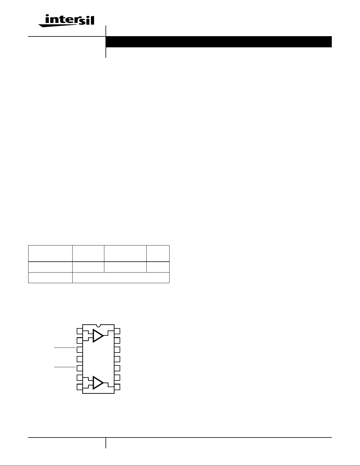
Pinout
HFA1245
(PDIP)
TOP VIEW
-IN1
+IN1
DISABLE 1
DISABLE 2
+IN2
-IN2
1
+
2
3
V-
4
5
6
+
-
7
14
OUT1
13
NC
12
GND
11
V+
10
NC
9
NC
8
OUT2
• Video Multiplexers
• Video Switching and Routing
• Professional Video Processing
• Video Digitizing Boards/Systems
• Multimedia Systems
• RGB Preamps
• Medical Imaging
• Hand Held and Miniaturized RF Equipment
• Battery Powered Communications
• High Speed Oscilloscopes and Analyzers
1
CAUTION: These devices are sensitive to electrostatic discharge; follow proper IC Handling Procedures.
1-888-INTERSIL or 321-724-7143
| Copyright © Intersil Corporation 1999
HFA1245
Absolute Maximum Ratings Thermal Information
Voltage Between V+ and V-. . . . . . . . . . . . . . . . . . . . . . . . . . . . 11V
DC Input Voltage . . . . . . . . . . . . . . . . . . . . . . . . . . . . . . . . V
Differential Input Voltage . . . . . . . . . . . . . . . . . . . . . . . . . . . . . . . 8V
Output Current (Note 2). . . . . . . . . . . . . . . . Short Circuit Protected
30mA Continuous
60mA ≤ 50% Duty Cycle
ESD Rating
Human Body Model (Per MIL-STD-883 Method 3015.7). . . 600V
SUPPLY
Operating Conditions
Temperature Range. . . . . . . . . . . . . . . . . . . . . . . . . . -40oC to 85oC
CAUTION: Stresses above those listed in “Absolute Maximum Ratings” may cause permanent damage to the device. This is a stress only rating and operation of the
device at these or any other conditions above those indicated in the operational sections of this specification is not implied.
NOTES:
1. θJA is measured with the component mounted on an evaluation PC board in free air.
2. Output is shortcircuitprotected to ground.Briefshort circuits togroundwill not degradereliability,however continuous (100%duty cycle) output
current must not exceed 30mA for maximum reliability.
Thermal Resistance (Typical, Note 1) θJA (oC/W)
PDIP Package . . . . . . . . . . . . . . . . . . . . . . . . . . . . . 100
Maximum Junction Temperature (Die) . . . . . . . . . . . . . . . . . . . 175oC
Maximum Junction Temperature (Plastic Package) . . . . . . . 150oC
Maximum Storage Temperature Range. . . . . . . . . . -65oC to 150oC
Maximum Lead Temperature (Soldering 10s) . . . . . . . . . . . . 300oC
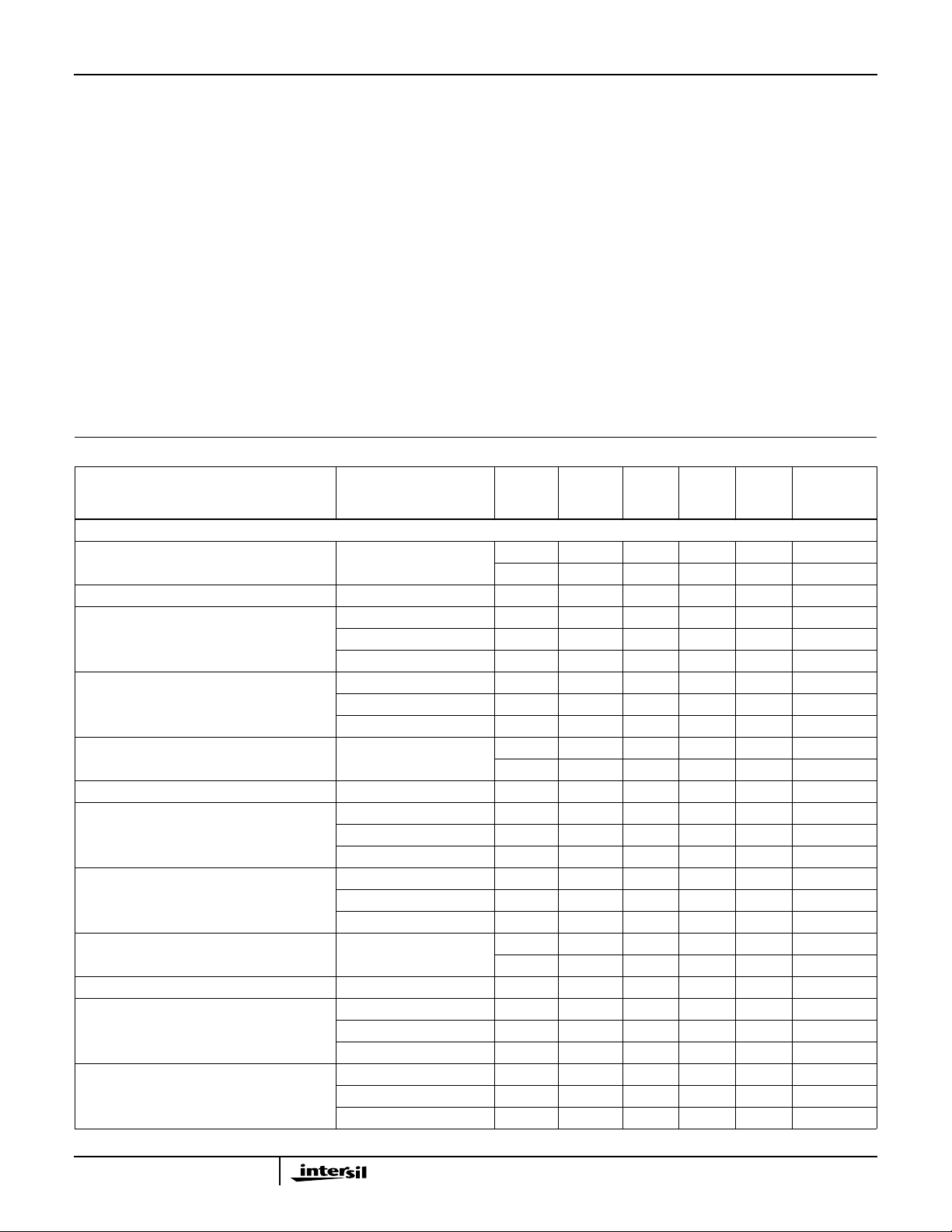
Electrical Specifications V
PARAMETER TEST CONDITIONS
INPUT CHARACTERISTICS
Input Offset Voltage A 25 - 2 5 mV
Average Input Offset Voltage Drift B Full - 1 10 µV/oC
Input Offset Voltage
Common-Mode Rejection Ratio
Input Offset Voltage
Power Supply Rejection Ratio
Non-Inverting Input Bias Current A 25 - 6 15 µA
Non-Inverting Input Bias Current Drift B Full - 5 60 nA/oC
Non-Inverting Input Bias Current
Power Supply Sensitivity
Non-Inverting Input Resistance ∆VCM = ±1.8V A 25 0.8 2 - MΩ
Inverting Input Bias Current A 25 - 2 7.5 µA
Inverting Input Bias Current Drift B Full - 60 200 nA/oC
Inverting Input Bias Current
Common-Mode Sensitivity
Inverting Input Bias Current
Power Supply Sensitivity
= ±5V, AV = +1, RF = 560Ω, RS = 650Ω, RL = 100Ω, Unless Otherwise Specified
SUPPLY
(NOTE 3)
TEST
LEVEL
A Full - 3 8 mV
∆VCM = ±1.8V A 25 45 48 - dB
∆VCM = ±1.8V A 85 43 46 - dB
∆VCM = ±1.2V A -40 43 46 - dB
∆VPS = ±1.8V A 25 48 52 - dB
∆VPS = ±1.8V A 85 46 50 - dB
∆VPS = ±1.2V A -40 46 50 - dB
A Full - 10 25 µA
∆VPS = ±1.8V A 25 - 0.5 1 µA/V
∆VPS = ±1.8V A 85 - 0.8 3 µA/V
∆VPS = ±1.2V A -40 - 0.8 3 µA/V
∆VCM = ±1.8V A 85 0.5 1.3 - MΩ
∆VCM = ±1.2V A -40 0.5 1.3 - MΩ
A Full - 5 15 µA
∆VCM = ±1.8V A 25 - 3 6 µA/V
∆VCM = ±1.8V A 85 - 4 8 µA/V
∆VCM = ±1.2V A -40 - 4 8 µA/V
∆VPS = ±1.8V A 25 - 2 5 µA/V
∆VPS = ±1.8V A 85 - 4 8 µA/V
∆VPS = ±1.2V A -40 - 4 8 µA/V
TEMP.
(oC) MIN TYP MAX UNITS
2
HFA1245
Electrical Specifications V
= ±5V, AV = +1, RF = 560Ω, RS = 650Ω, RL = 100Ω, Unless Otherwise Specified (Continued)
SUPPLY
(NOTE 3)
PARAMETER TEST CONDITIONS
TEST
LEVEL
TEMP.
(oC) MIN TYP MAX UNITS
Inverting Input Resistance B 25 - 56 - Ω
Input Capacitance B 25 - 2.0 - pF
Input Voltage Common Mode Range
(Implied byVIOCMRR, +RIN, and-I
Tests)
BIAS
CMS
A 25, 85 ±1.8 ±2.4 - V
A -40 ±1.2 ±1.7 - V
Input Noise Voltage Density (Note 6) f = 100kHz B 25 - 3.5 - nV/√Hz
Non-Inverting Input Noise Current Density
f = 100kHz B 25 - 2.5 - pA/√Hz
(Note 6)
Inverting Input Noise Current Density
f = 100kHz B 25 - 30 - pA/√Hz
(Note 6)
TRANSFER CHARACTERISTICS
Open Loop Transimpedance Gain (Note 6) B 25 - 500 - kΩ
AC CHARACTERISTICS
-3dB Bandwidth (V
OUT
= 0.2V
, Note 6) AV = +1, +RS = 650Ω B 25 - 260 - MHz
P-P
AV = +2, RF= 750Ω B 25 - 420 - MHz
AV = -1, RF = 475Ω B 25 - 280 - MHz
Full Power Bandwidth
(V
4V
OUT
P-P
= 5V
at AV = +2/-1,
P-P
at AV = +1, Note 6)
Gain Flatness (AV = +2, RF = 750Ω,
V
OUT
= 0.2V
P-P
, Note 6)
AV = +1, +RS = 650Ω B 25 - 150 - MHz
AV = +2, RF= 750Ω B 25 - 115 - MHz
AV = -1, RF = 475Ω B 25 - 160 - MHz
To 25MHz B 25 - ±0.04 - dB
To 50MHz B 25 - ±0.11 - dB
Minimum Stable Gain A Full - 1 - V/V
Crosstalk (AV = +2, RF= 750Ω,
V
OUT
= 1V
, Notes 4, 6)
P-P
5MHz B 25 - -83 - dB
10MHz B 25 - -77 - dB
OUTPUT CHARACTERISTICS AV = +2, RF = 750Ω, Unless Otherwise Specified
Output Voltage Swing (Note 6) AV = -1, RL = 100Ω A25±3 ±3.4 - V
A Full ±2.8 ±3- V
Output Current (Note 6) AV = -1, RL = 50Ω A 25, 85 50 60 - mA
A -40 28 42 - mA
Output Short Circuit Current B 25 - 90 - mA
Closed Loop Output Resistance (Note 6) DC B 25 - 0.07 - Ω
Second Harmonic Distortion
(V
OUT
= 2V
P-P
)
Third Harmonic Distortion
(V
OUT
= 2V
P-P
)
10MHz B 25 - -50 - dBc
20MHz B 25 - -45 - dBc
10MHz B 25 - -57 - dBc
20MHz B 25 - -50 - dBc
3rd Order Intercept (Note 6) 20MHz B 25 - 23 - dBm
Reverse Isolation (S12, Note 6) 65MHz B 25 - 60 - dB
TRANSIENT CHARACTERISTICS AV = +2, RF = 750Ω, Unless Otherwise Specified
Rise and Fall Times (V
OUT
= 0.5V
) Rise Time B 25 - 0.9 - ns
P-P
Fall Time B 25 - 1.5 - ns
Overshoot
(V
= 0.5V
OUT
Slew Rate (V
P-P
OUT
, VIN t
= 4V
P-P
RF = 560Ω, +RS = 650Ω)
= 1ns, Note 5)
RISE
, AV = +1,
+OS B 25 - 5 - %
-OS B 25 - 10 - %
+SR B 25 - 1150 - V/µs
-SR (Note 7) B 25 - 800 - V/µs
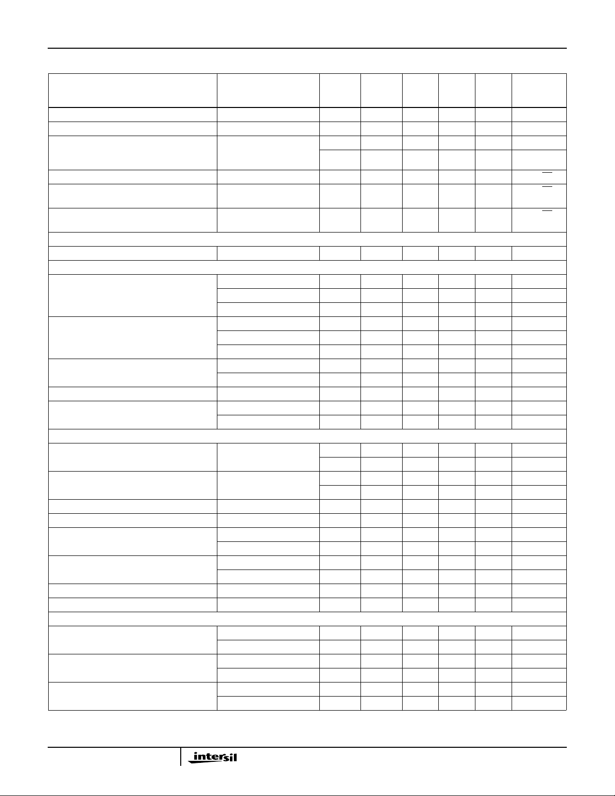
3
HFA1245
Electrical Specifications V
= ±5V, AV = +1, RF = 560Ω, RS = 650Ω, RL = 100Ω, Unless Otherwise Specified (Continued)
SUPPLY
(NOTE 3)
Slew Rate (V
PARAMETER TEST CONDITIONS
OUT
= 5V
, AV = +2) +SR B 25 - 1400 - V/µs
P-P
TEST
LEVEL
TEMP.
(oC) MIN TYP MAX UNITS
-SR (Note 7) B 25 - 800 - V/µs
Slew Rate
(V
= 5V
OUT
P-P
Settling Time (V
Note 6)
, AV = -1, RF = 475Ω)
= +2V to 0V step,
OUT
+SR B 25 - 2200 - V/µs
-SR (Note 7) B 25 - 1200 - V/µs
To 0.1% B 25 - 15 - ns
To 0.05% B 25 - 20 - ns
To 0.02% B 25 - 40 - ns
Overdrive Recovery Time VIN = ±2V B 25 - 8.5 - ns
VIDEO CHARACTERISTICS AV = +2, RF = 750Ω, Unless Otherwise Specified
Differential Gain (f = 3.58MHz) RL = 150Ω B 25 - 0.02 - %
RL = 75Ω B 25 - 0.03 - %
Differential Phase (f = 3.58MHz) RL = 150Ω B 25 - 0.03 - Degrees
RL = 75Ω B 25 - 0.05 - Degrees
DISABLE CHARACTERISTICS
Disabled Supply Current V
DISABLE
= 0V A Full - 3 4 mA/Op Amp
DISABLE Input Logic Voltage Low A Full - - 0.8 V
High A 25, 85 2.0 - - V
A -40 2.4 - - V
DISABLE Input Logic Low Current V
DISABLE Input Logic High Current V
Output Disable Time (Note 6) V
Output Enable Time (Note 6) V
Disabled Output Capacitance V
Disabled Output Leakage (Note 6) V
All Hostile Off Isolation (V
VIN = 1V
, AV = +2, Note 6)
P-P
DISABLE
= 0V,
DISABLE
DISABLE
OUT
V
DISABLE
OUT
V
DISABLE
DISABLE
DISABLE
VIN = +2V, V
At 5MHz B 25 - 65 - dB
At 10MHz B 25 - 60 - dB
= 0V A Full - 100 200 µA
= 5V A Full - 1 15 µA
= ±1V,
B 25 - 30 - ns
= 2.4V to 0.4V
= ±1V,
B 25 - 150 - ns
= 0.4V to 2.4V
= 0V B 25 - 4.5 - pF
= 0V,
OUT
= ±3V
A Full - 2 10 µA
POWER SUPPLY CHARACTERISTICS
Power Supply Range C 25 ±4.5 - ±5.5 V
Power Supply Current (Note 6) A 25 5.6 5.8 6.1 mA/Op Amp
A Full 5.4 5.9 6.3 mA/Op Amp
NOTES:
3. Test Level: A. Production Tested; B. Typical or Guaranteed Limit Based on Characterization; C. Design Typical for Information Only.
4. The typical use for these amplifiers is in multiplexed configurations, where one amplifier (hostile channel) is enabled, and the passive channel
is disabled.Thecrosstalk data specified is testedinthis manner, with theinputsignal applied to thehostilechannel, while monitoring the output
of the passive channel. Crosstalk performance with both the hostile and passive channels enabled is typically -63dB at 5MHz, and -58dB at
10MHz.
5. Undershoot dominates for output signal swings below GND (e.g., 0.5V
V
= 0V to 0.5V condition. See the “Application Information“ section for details.
OUT
), yielding a higher overshoot limit compared to the
P-P
6. See Typical Performance Curves for more information.
7. Slew rates are asymmetrical if the output swings below GND (e.g., a bipolar signal). Positive unipolar output signals have symmetric positive
and negative slew rates comparable to the +SR specification. See the “Application Information” section, and the pulse response graphs for
details.
4
HFA1245
Application Information
Relevant Application Notes
The following Application Notes pertain to the HFA1245:
• AN9787-An Intuitive Approach to Understanding
Current Feedback Amplifiers
• AN9420-Current Feedback Amplifier Theory and
Applications
• AN9663-Converting from Voltage Feedback to Current
Feedback Amplifiers
These publications may be obtained from Intersil’s web site
(http://www.intersil.com) or via our AnswerFAX system.
Optimum Feedback Resistor
Although a current feedback amplifier’s bandwidth
dependency on closed loop gain isn’t as severe as that of a
voltage feedback amplifier, there can be an appreciable
decrease in bandwidth at higher gains. This decrease may
be minimized by taking advantage of the current feedback
amplifier’s unique relationship between bandwidth and R
All current feedback amplifiers require a feedback resistor,
even for unity gain applications, and R
, in conjunction with
F
the internal compensation capacitor, sets the dominant pole
of the frequency response.Thus,theamplifier’s bandwidth is
inversely proportional to R
optimized for a 750Ω R
. The HFA1245 design is
F
at a gain of +2. Decreasing R
F
decreases stability, resulting in excessive peaking and
overshoot (Note: Capacitive feedback will cause the same
problemsduetothefeedbackimpedancedecreaseathigher
frequencies). At higher gains the amplifier is more stable, so
R
can be decreased in a trade-off of stability for bandwidth.
F
The table below lists recommended RF values for v arious
gains, and the expected bandwidth. F or good channel-tochannel gain matching, it is recommended that all resistors
(termination as well as gain setting) be ±1% tolerance or
better. Note that a series input resistor, on +IN, is required for
a gain of +1, to reduce gain peaking and increase stability.
TABLE 1. OPTIMUM FEEDBACK RESISTOR
GAIN
(AV)R
-1 475 280
+1 560 (+RS = 650Ω) 260
+2 750 420
+5 200 270
+10 180 140
F
(Ω)
BANDWIDTH
(MHz)
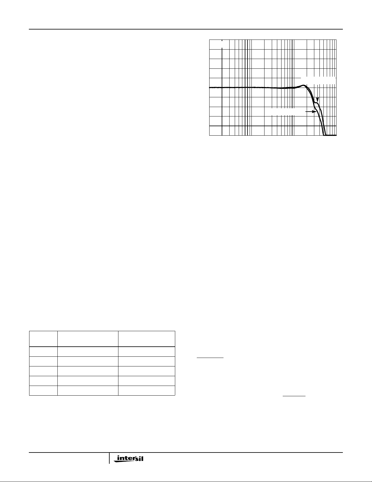
Channel-T o-Channel Frequenc y Response Matching
The frequency response of channel 1 and channel 2 aren’t
perfectly matched. For the best channel-to-channel
frequency response match in a gain of 2 (see Figure 1), use
R
= 650Ω for channel 1 and RF = 806Ω for channel 2.
F
.
F
F
AV = +2
2
1
0
-1
-2
-3
NORMALIZED GAIN (dB)
-4
1 10 100 1000
FREQUENCY (MHz)
FIGURE 1. CHANNEL 1 AND CHANNEL2MATCHED
FREQUENCY RESPONSE
RF = 650Ω, CH1
RF = 806Ω, CH2
Non-inverting Input Source Impedance
For best operation, the DC source impedance seen by the
non-inverting input should be ≥50Ω. This is especially
important in inverting gain configurations where the
non-inverting input would normally be connected directly to
GND.
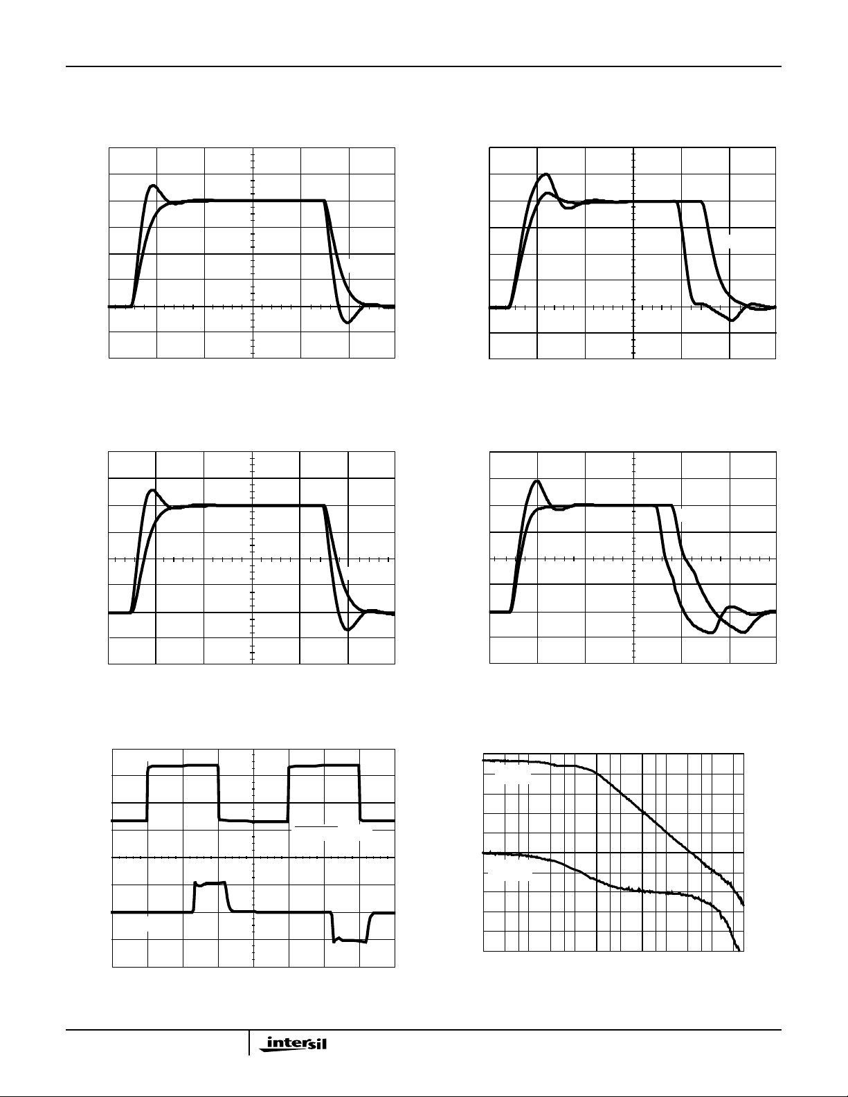
Pulse Undershoot and Asymmetrical Slew Rates
The HFA1245 utilizes a quasi-complementary output stage
to achieve high output current while minimizing quiescent
supply current. In this approach, a composite device
replaces the traditional PNP pulldown transistor. The
composite device switches modes after crossing 0V,
resulting in added distortion for signals swinging below
ground, and an increased undershoot on the negative
portion of the output waveform (see Figures 7, 11, 15, and
19). This undershoot isn’t present for small bipolar signals,
or large positive signals. Another artifact of the composite
device is asymmetrical slew rates for output signals with a
negative voltage component. The slew rate degrades as the
output signal crosses through 0V (see Figures 7, 11, 15, and
19), resulting in a slower overall negative slew rate. Positive
only signals have symmetrical slew rates as illustrated in the
large signal positive pulse response graphs (see Figures 5,
9, 13, and 17).
DISABLE Input TTL Compatibility
The HF A1245 deriv es an internal GND ref erence for the
digital circuitry as long as the power supplies are symmetrical
about GND. With symmetrical supplies the digital switching
threshold (V
ensures the TTL compatibility of the
asymmetrical supplies (e.g., +10V, 0V) are utilized, the
switching threshold becomes:
V+ V-+
V
------------------- 1.4V,+=
TH
and the V
=(VIH+VIL)/2 = (2.0 + 0.8)/2) is 1.4V, which
TH
DISABLE input. If
2
and VIL levels will be VTH±0.6V, respectively.
IH
5
HFA1245
Optional GND Pin for TTL Compatibility
Pin 12 is an optional GND reference used to ensure the TTL
compatibility of the
DISABLE inputs. With symmetrical
supplies the GND pin may be unconnected, or connected
directly to GND. If asymmetrical supplies (e.g., +10V, 0V) are
utilized, and TTL compatibility is desired, the GND pin must
be connected to GND.With an external GND, the
DISABLE
input is TTL compatible regardless of supply voltage utilized.
PC Board Layout
The HFA1245’s frequency response depends greatly on the
care taken in designing the PC board. The use of low
inductance components such as chip resistors and chip
capacitors is strongly recommended, while a solid
ground plane is a must!
Attention should be given to decoupling the power supplies.
A large value (10µF) tantalum in parallel with a small value
(0.1µF) chip capacitor works well in most cases.
Terminated microstrip signal lines are recommended at the
input and output of the device. Capacitance directly on the
output must be minimized, or isolated as discussed in the
next section.
Care must also be taken to minimize the capacitance to
ground at the amplifier’s inverting input (-IN), as this
capacitance causes gain peaking, pulse overshoot, and if
large enough, instability. To reduce this capacitance, the
designer should remove the ground plane under traces
connected to -IN, and keep connections to -IN as short as
possible.
An example of a good high frequency layout is the HA5022
evaluation board discussed below.
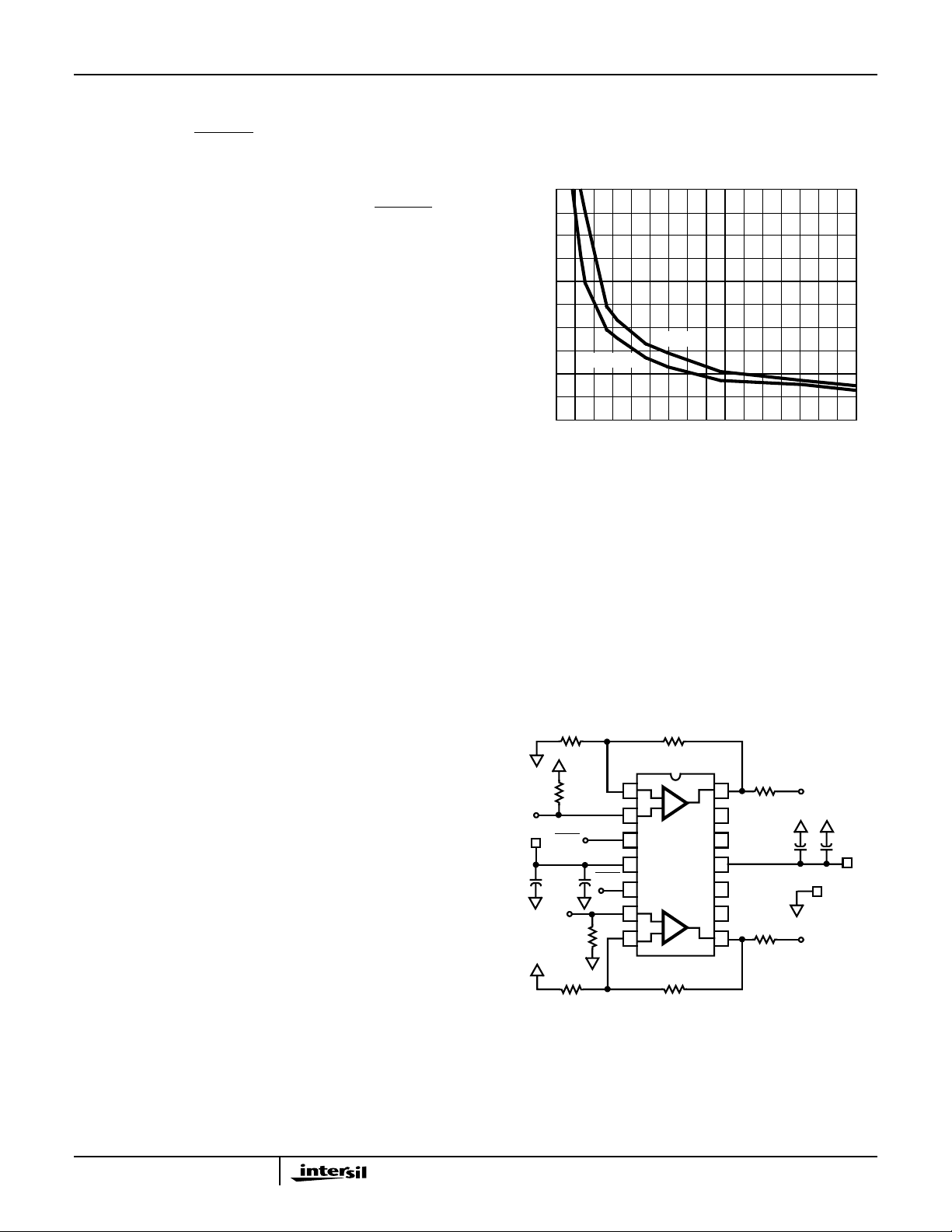
Driving Capacitive Loads
Capacitive loads, such as an A/D input, or an improperly
terminated transmission line degrade the amplifier’s phase
margin resulting in frequency response peaking and
possible oscillations. In most cases, the oscillation can be
avoided by placing a resistor (R
prior to the capacitance.
Figure 2 details starting points for the selection of this
resistor. The points on the curve indicate the R
combinations for the optimum bandwidth, stability, and
settling time, but experimental fine tuning is recommended.
Picking a point above or to the right of the curve yields an
overdampedresponse,whilepointsbelow or left of the curve
indicate areas of underdamped performance.
R
and CLform a low pass network at the output, thus
S
limiting system bandwidth well below the amplifier
bandwidth of 260MHz (for A
C
increases (as illustrated in the curves), the maximum
L
bandwidth is obtained without sacrificing stability. Even so,
bandwidth still decreases as the load capacitance
) in series with the output
S
and C
S
= +1). By decreasing RS as
V
L
increases. For example, at A
= +1, RS = 45Ω, CL = 40pF,
V
the overall bandwidth is 185MHz, but the bandwidth drops
to 85MHz at A
50
40
30
20
10
SERIES OUTPUT RESISTANCE (Ω)
0
0 100 200 300 400
FIGURE 2. RECOMMENDED SERIES OUTPUTRESISTOR vs
= +1, RS = 9Ω, CL = 330pF.
V
AV = +1
AV = +2
150 250 35050
LOAD CAPACITANCE (pF)
LOAD CAPACITANCE
Evaluation Board
Evaluate the HFA1245’s performance using the HA5022
evaluation board (part number HA5022EVAL). Please
contact your local sales office for ordering information. The
feedback and gain setting resistors must be replaced with
the appropriate value (see “Optimum Feedback Resistor”
table) for the gain being evaluated. Also, replace the two 0
series output resistors (RS) with 50Ω resistors.
The modified schematic of the board is shown in Figure 3.
750Ω
50Ω
IN1
DIS1
-5V
DIS2
0.1µF10µF
IN2
50Ω
750Ω
FIGURE 3. EVALUATION BOARD SCHEMATIC MODIFIED
FOR AV = +2
750Ω
1
-
+
2
CH1
3
4
5
CH2
6
+
-
7
750Ω
50Ω
14
R
13
NC
GND
12
11
10
NC
9
NC
50Ω
8
R
OUT1
S
10µF0.1µF
+5V
GND
OUT2
S
Ω
6
HFA1245
Typical Performance Curves V
= ±5V, TA = 25oC, RF= Value From the Optimum Feedback Resistor Table, RL = 100Ω,
SUPPLY
Unless Otherwise Specified
300
250
200
150
100
50
OUTPUT VOLTAGE (mV)
0
-50
-100
AV = +2
TIME (5ns/DIV.)
3.0
2.5
2.0
1.5
1.0
0.5
OUTPUT VOLTAGE (V)
0
-0.5
-1.0
AV = +2
TIME (5ns/DIV.)
FIGURE 4. SMALL SIGNAL POSITIVE PULSE RESPONSE FIGURE 5. LARGE SIGNAL POSITIVE PULSE RESPONSE
200
150
100
50
AV = +2
2.0
1.5
1.0
0.5
AV = +2
0
-50
OUTPUT VOLTAGE (mV)
-100
-150
-200
TIME (5ns/DIV.)
-0.5
OUTPUT VOLTAGE (V)
-1.0
-1.5
-2.0
0
TIME (5ns/DIV.)
FIGURE 6. SMALL SIGNAL BIPOLAR PULSE RESPONSE FIGURE 7. LARGE SIGNAL BIPOLAR PULSE RESPONSE
300
AV = +1
250
200
150
100
50
OUTPUT VOLTAGE (mV)
0
3.0
AV = +1
2.5
2.0
1.5
1.0
0.5
OUTPUT VOLTAGE (V)
0
-50
-100
TIME (5ns/DIV.)
-0.5
-1.0
TIME (5ns/DIV.)
FIGURE 8. SMALL SIGNAL POSITIVE PULSE RESPONSE FIGURE 9. LARGE SIGNAL POSITIVE PULSE RESPONSE
7

HFA1245
Typical Performance Curves V
= ±5V, TA = 25oC, RF= Value From the Optimum Feedback Resistor Table, RL = 100Ω,
SUPPLY
Unless Otherwise Specified (Continued)
200
AV = +1
150
100
50
0
-50
-100
OUTPUT VOLTAGE (mV)
-150
-200
TIME (5ns/DIV.)
FIGURE 10. SMALL SIGNAL BIPOLAR PULSE RESPONSE
300
AV = -1
250
2.0
AV = +1
1.5
1.0
0.5
0
-0.5
OUTPUT VOLTAGE (V)
-1.0
-1.5
-2.0
TIME (5ns/DIV.)
FIGURE 11. LARGE SIGNAL BIPOLAR PULSE RESPONSE
3.0
AV = -1
2.5
200
150
100
50
0
OUTPUT VOLTAGE (mV)
-50
-100
TIME (5ns/DIV.)
2.0
1.5
1.0
0.5
OUTPUT VOLTAGE (V)
-0.5
-1.0
0
TIME (5ns/DIV.)
FIGURE 12. SMALL SIGNAL POSITIVE PULSE RESPONSE FIGURE 13. LARGE SIGNAL POSITIVE PULSE RESPONSE
200
150
100
50
0
-50
-100
OUTPUT VOLTAGE (mV)
-150
-200
AV = -1
TIME (5ns/DIV.)
2.0
1.5
1.0
0.5
-0.5
OUTPUT VOLTAGE (V)
-1.0
-1.5
-2.0
AV = -1
0
TIME (5ns/DIV.)
FIGURE 14. SMALL SIGNAL BIPOLAR PULSE RESPONSE FIGURE 15. LARGE SIGNAL BIPOLAR PULSE RESPONSE
8
HFA1245
Typical Performance Curves V
= ±5V, TA = 25oC, RF= Value From the Optimum Feedback Resistor Table, RL = 100Ω,
SUPPLY
Unless Otherwise Specified (Continued)
300
250
200
150
100
50
0
OUTPUT VOLTAGE (mV)
-50
-100
AV = +5
AV = +10
TIME (5ns/DIV.)
3.0
2.5
2.0
1.5
1.0
0.5
OUTPUT VOLTAGE (V)
-0.5
-1.0
AV = +5
AV = +10
0
TIME (5ns/DIV.)
FIGURE 16. SMALL SIGNAL POSITIVE PULSE RESPONSE FIGURE 17. LARGE SIGNAL POSITIVE PULSE RESPONSE
200
150
100
AV = +5
50
2.0
1.5
1.0
0.5
AV = +5
AV = +10
0
-50
-100
OUTPUT VOLTAGE (mV)
-150
-200
AV = +10
TIME (5ns/DIV.)
-0.5
-1.0
OUTPUT VOLTAGE (V)
-1.5
-2.0
0
TIME (5ns/DIV.)
FIGURE 18. SMALL SIGNAL BIPOLAR PULSE RESPONSE FIGURE 19. LARGE SIGNAL BIPOLAR PULSE RESPONSE
3.0
2.0
1.0
1.0
VOLTAGE (V)
-1.0
0
0
AV = +2
DISABLE INPUT
OUTPUT
TIME (100ns/DIV.)
630
200
63
20
6.3
2
GAIN (kΩ)
PHASE
0.63
0.2
0.063
0.001 0.01
GAIN
36
0.1
FREQUENCY (MHz)
1
180
135
90
45
0
10
100
500
PHASE (DEGREES)
FIGURE 20.
OUTPUT DISABLE / ENABLE RESPONSE
9
FIGURE 21. OPEN LOOP TRANSIMPEDANCE
HFA1245
Typical Performance Curves V
SUPPLY
Unless Otherwise Specified (Continued)
V
3
GAIN
0
GAIN (dB)
-3
-6
PHASE
OUT
= 200mV
P-P
AV = +1, CH1
AV = +1, CH2
AV = -1
AV = +1
BOTH CHANNELS SHOWN
AV = -1
1 10 100 1000
FREQUENCY (MHz)
FIGURE 22. FREQUENCY RESPONSE
V
P-P
OUT
P-P
P-P
= 1V
P-P
P-P
= 1V
P-P
AV = +2
3
GAIN
0
-3
-6
PHASE
V
OUT
= 1V
V
P-P
OUT
V
OUT
, CH1
= 2.5V
= 4V
NORMALIZED GAIN (dB)
V
= 4V
OUT
V
= 2.5V
OUT
V
OUT
BOTH CHANNELS SHOWN
1 10 100 1000
FREQUENCY (MHz)
= ±5V, TA = 25oC, RF= Value From the Optimum Feedback Resistor Table, RL = 100Ω,
V
0
90
180
270
= 200mV
-3
-6
3
0
OUT
GAIN
PHASE
P-P
AV = +2, CH1
NORMALIZED GAIN (dB)
AV = +10
AV = +10
AV = +5
AV = +2, CH2
AV = +5
AV = +2
360
NORMALIZED PHASE (DEGREES)
BOTH CHANNELS SHOWN
1 10 100 1000
FREQUENCY (MHz)
FIGURE 23. FREQUENCY RESPONSE
, CH2
0
90
180
270
360
PHASE (DEGREES)
AV = +1
3
GAIN
0
GAIN (dB)
-3
-6
PHASE
V
V
OUT
V
OUT
V
OUT
OUT
= 2.5V
= 4V
= 4V
= 2.5V
V
OUT
P-P
= 1V
P-P
P-P
V
P-P
OUT
P-P
=1V
P-P
BOTH CHANNELS SHOWN
1 10 100 1000
FREQUENCY (MHz)
0
2
2
90
180
270
360
PHASE (DEGREES)
0
90
180
270
PHASE (DEGREES)
360
FIGURE24. FREQUENCYRESPONSEFORVARIOUSOUTPUT
VOLTAGES
V
3
AV = -1
OUT
=1V
P-P
GAIN
V
=4V
OUT
V
V
OUT
=4V
OUT
P-P
= 2.5V
V
OUT
P-P
= 2.5V
=1V
P-P
P-P
P-P
0
90
180
270
360
GAIN (dB)
-3
-6
PHASE
BOTH CHANNELS SHOWN
V
OUT
1 10 100 1000
FREQUENCY (MHz)
FIGURE26. FREQUENCYRESPONSEFORVARIOUSOUTPUT
VOLTAGES
10
FIGURE25. FREQUENCYRESPONSEFORVARIOUSOUTPUT
VOLTAGES
BOTH CHANNELS SHOWN
3
0
-3
-6
NORMALIZED GAIN (dB)
-9
NORMALIZED PHASE (DEGREES)
1 10 100 1000
FIGURE 27. FULL POWER BANDWIDTH
AV = +2, V
AV = +1, V
AV = -1, V
FREQUENCY (MHz)
OUT
= 5V
OUT
OUT
P-P
= 4V
= 5V
P-P
P-P

HFA1245
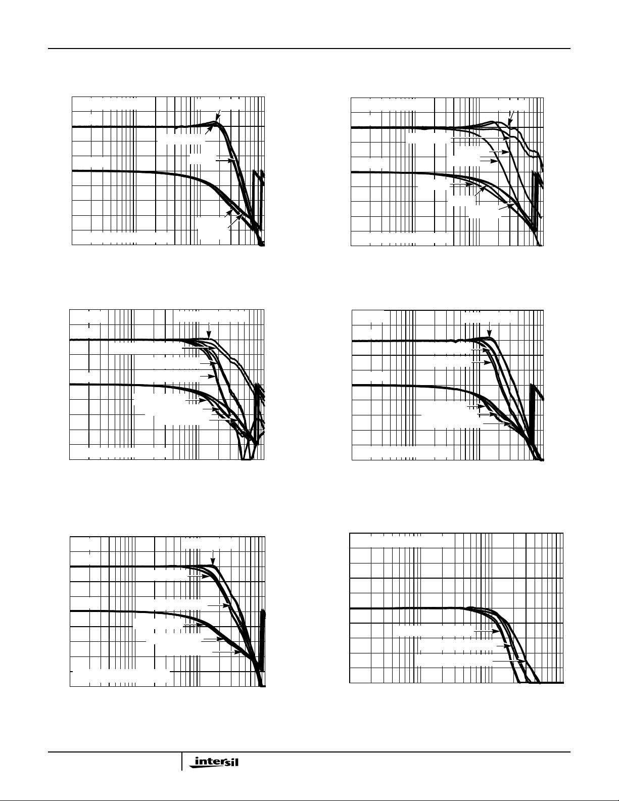
Typical Performance Curves V
SUPPLY
Unless Otherwise Specified (Continued)
V
= 200mV
OUT
0.4
0.3
0.2
0.1
0
-0.1
-0.2
NORMALIZED GAIN (dB)
-0.3
-0.4
BOTH CHANNELS SHOWN
1 10 100
P-P
AV = +1, CH2
AV = +1, CH1
AV = +2, CH2
AV = +2, CH1
FREQUENCY (MHz)
FIGURE 28. GAIN FLATNESS FIGURE 29. CROSSTALK (PASSIVE CHANNEL ENABLED)
-20
-30
-40
-50
-60
-70
CROSSTALK (dB)
-80
-90
-100
AV = +2, VIN = 1V
P-P
= ±5V, TA = 25oC, RF= Value From the Optimum Feedback Resistor Table, RL = 100Ω,
AV = -1
AV = +2, VIN = 1V
-20
-30
-40
-50
-60
-70
CROSSTALK (dB)
-80
-90
-100
0.3 1 10 100 1000
AV = +2, VIN = 1V
20
DIS1 = DIS2 = 0V
30
40
50
60
70
80
OFF ISOLATION (dB)
90
100
P-P
FREQUENCY (MHz)
P-P
0.3 1 10 100 1000
FREQUENCY (MHz)
FIGURE 30. CROSSTALK (PASSIVE CHANNEL DISABLED)
10
20
30
40
50
60
GAIN (dB)
70
80
90
100
1 10 100 1000
FREQUENCY (MHz)
AV = +2
AV = -1
AV = +1
FIGURE 32. REVERSE ISOLATION
11
0.3 1 10 100 1000
FREQUENCY (MHz)
FIGURE 31. ALL HOSTILE OFF ISOLATION
AV = +2
1K
100
10
1
0.1
0.01
OUTPUT RESISTANCE (Ω)
0.3 1 10 100
FREQUENCY (MHz)
FIGURE 33. ENABLED OUTPUT RESISTANCE
1000

HFA1245
Typical Performance Curves V
= ±5V, TA = 25oC, RF= Value From the Optimum Feedback Resistor Table, RL = 100Ω,
SUPPLY
Unless Otherwise Specified (Continued)
35
AV = +2
30
25
20
TOI (dBm)
15
10
5
0 50 100 150
FREQUENCY (MHz)
0.1
0.05
0.025
0
-0.025
-0.05
SETTLING ERROR (%)
-0.1
3132333435363738393103
TIME (ns)
FIGURE 34. 3rd ORDER INTERCEPT vs FREQUENCY FIGURE 35. SETTLING TIME RESPONSE
100
I
NI-
I
NI+
10
E
NI
NOISE VOLTAGE (nV/√Hz)
1
0.1 1 10 100
FREQUENCY (kHz)
100
Hz)
10
NOISE CURRENT (pA/√
1
3.6
A
= -1
V
3.5
3.4
3.3
3.2
3.1
3.0
2.9
OUTPUT VOLTAGE (V)
2.8
2.7
2.6
-50 -25 0 25 50 75 100 125
|-V
| (RL = 50Ω)
OUT
+V
+V
OUT
OUT
|-V
OUT
(RL = 100Ω)
(RL = 50Ω)
TEMPERATURE (
| (RL = 100Ω)
V
= 2V
OUT
AV = +2
R
= 750Ω
F
o
C)
FIGURE 36. INPUT NOISE CHARACTERISTICS
30
-55oC
25
20
15
o
125
C
10
25oC
5
TOTAL SUPPLY CURRENT (mA)
-55oC
0
345678
SUPPLY VOLTAGE (±V)
25oC
125oC
FIGURE 38. SUPPLY CURRENT vs SUPPLY VOLTAGE
12
FIGURE 37. OUTPUT VOLTAGE vs TEMPERATURE
1
V
= 0V
DIS
0.9
V
0.8
0.7
0.6
0.5
0.4
0.3
V
= 3.5V, VIN = -2.5V
OUT
0.2
OUTPUT LEAKAGE CURRENT (µA)
0.1
0
-75 -50 0 50 100 125
-25
= -3.5V, VIN = 2.5V
OUT
V
= -3V, VIN = 2V
OUT
V
= 3V, VIN = -2V
OUT
25
TEMPERATURE (
75
o
C)
FIGURE 39. DISABLED OUTPUT LEAKAGE vs TEMPERATURE

Die Characteristics
HFA1245
DIE DIMENSIONS:
69 mils x 92 mils x 19 mils
1750µm x 2330µm x 483µm
METALLIZATION:
Type: Metal 1: AICu(2%)/TiW
Thickness: Metal 1: 8k
Å ±0.4kÅ
Type: Metal 2: AICu(2%)
Thickness: Metal 2: 16k
Å ±0.8kÅ
Metallization Mask Layout
+IN1
SUBSTRATE POTENTIAL (POWERED UP):
PASSIVATION:
TRANSISTOR COUNT:
HFA1245
-IN1 OUT1
Floating (Recommend Connection to V-)
Type: Nitride
Thickness: 4k
Å ±0.5kÅ
180
GND (NOTE 8)
V+
DISABLE1
V-
DISABLE2
+IN2
-IN2
NOTE:
8. This is an optional GND pad. Users may set a GND reference, via this pad, to ensure the TTL compatibility of the DISABLE inputs when using
asymmetrical supplies (e.g., V+ = 10V, V- = 0V). See the “Application Information” section for details.
V-
NC
NC
OUT2
13

Dual-In-Line Plastic Packages (PDIP)
HFA1245
N
D1
E1
-B-
-C-
A1
A2
E
A
L
e
C
C
L
e
A
C
e
B
INDEX
AREA
BASE
PLANE
SEATING
PLANE
D1
B1
1 2 3 N/2
-AD
e
B
0.010 (0.25) C AM BS
NOTES:
1. Controlling Dimensions: INCH. In case of conflictbetweenEnglish
and Metric dimensions, the inch dimensions control.
2. Dimensioning and tolerancing per ANSI Y14.5M-1982.
3. Symbols are definedin the “MOSeriesSymbol List”inSection 2.2of
Publication No. 95.
4. Dimensions A, A1 and L are measured with the package seatedin
JEDEC seating plane gauge GS-3.
5. D, D1, and E1 dimensions do not include mold flash orprotrusions.
Mold flash or protrusions shall not exceed 0.010 inch (0.25mm).
6. E and are measured with the leads constrained to be perpen-
e
dicular to datum .
A
-C-
7. eB and eC are measured at the lead tips with the leads unconstrained. eC must be zero or greater.
8. B1 maximumdimensionsdo notincludedambar protrusions.Dambar
protrusions shall not exceed 0.010 inch (0.25mm).
9. N is the maximum number of terminal positions.
10. Corner leads (1, N, N/2 and N/2 + 1) for E8.3, E16.3, E18.3, E28.3,
E42.6 will have a B1 dimension of 0.030 - 0.045 inch (0.76 -
1.14mm).
E14.3 (JEDEC MS-001-AA ISSUE D)
14 LEAD DUAL-IN-LINE PLASTIC PACKAGE
INCHES MILLIMETERS
SYMBOL
A - 0.210 - 5.33 4
A1 0.015 - 0.39 - 4
A2 0.115 0.195 2.93 4.95 -
B 0.014 0.022 0.356 0.558 B1 0.045 0.070 1.15 1.77 8
C 0.008 0.014 0.204 0.355 -
D 0.735 0.775 18.66 19.68 5
D1 0.005 - 0.13 - 5
E 0.300 0.325 7.62 8.25 6
E1 0.240 0.280 6.10 7.11 5
e 0.100 BSC 2.54 BSC e
A
e
B
0.300 BSC 7.62 BSC 6
- 0.430 - 10.92 7
L 0.115 0.150 2.93 3.81 4
N14 149
NOTESMIN MAX MIN MAX
Rev. 0 12/93
All Intersil semiconductor products are manufactured, assembled and tested under ISO9000 quality systems certification.
Intersil semiconductor products are soldby description only.Intersil Corporation reserves the rightto make changes in circuit design and/or specificationsat any time without notice. Accordingly, the reader is cautioned to verify that data sheets are current before placing orders.Information furnished by Intersil is believed to be accur ateand
reliable. Howe ver, no responsibilityis assumed by Intersil or its subsidiaries for its use; nor f orany infringements of patents or other rights of third parties which may result
from its use. No license is granted by implication or otherwise under any patent or patent rights of Intersil or its subsidiaries.
For information regarding Intersil Corporation and its products, see web site www.intersil.com
Sales Office Headquarters
NORTH AMERICA
Intersil Corporation
P. O. Box 883, Mail Stop 53-204
Melbourne, FL 32902
TEL: (321) 724-7000
FAX: (321) 724-7240
14
EUROPE
Intersil SA
Mercure Center
100, Rue de la Fusee
1130 Brussels, Belgium
TEL: (32) 2.724.2111
FAX: (32) 2.724.22.05
ASIA
Intersil (Taiwan) Ltd.
7F-6, No. 101 Fu Hsing North Road
Taipei, Taiwan
Republic of China
TEL: (886) 2 2716 9310
FAX: (886) 2 2715 3029
 Loading...