HFA1205
September 1998 File Number 3605.5
Dual, 400MHz, Low Power, Video
Operational Amplifier
The HFA1205 is a dual, high speed, low power current
feedback amplifier built with Intersil’s proprietary
complementary bipolar UHF-1 process.
These amplifiers deliver 400MHz bandwidth and 1275V/µs
slew rate, on only 60mW of quiescent power. They are
specifically designed to meet the performance, power, and
cost requirements of high volume video applications. The
excellent gain flatness and differential gain/phase
performance make these amplifiers well suited for
component or composite video applications. Video
performance is maintained even when driving a back
terminated cable (R
when driving two back terminated cables (R
= 150Ω), and degrades only slightly
L
=75Ω). RGB
L
applications will benefit from the high slew rates, and high
full power bandwidth.
The HFA1205 is a pin compatible, low power, high
performance upgrade for the popular Intersil HA5023. For a
dual amplifier with output disable capability, please see the
HFA1245 datasheet.
Ordering Information
PART NUMBER
(BRAND)
HFA1205IP -40 to 85 8 Ld PDIP E8.3
HFA1205IB
(H1205I)
HA5023EVAL High Speed Op Amp DIP Evaluation Board
TEMP.
RANGE (oC) PACKAGE
-40 to 85 8 Ld SOIC M8.15
PKG.
NO.
Features
• Low Supply Current . . . . . . . . . . . . . . . . . 5.8mA/Op Amp
• High Input Impedance . . . . . . . . . . . . . . . . . . . . . . . 2MΩ
• Wide -3dB Bandwidth (A
= +2). . . . . . . . . . . . . . 400MHz
V
• Very Fast Slew Rate. . . . . . . . . . . . . . . . . . . . . . 1275V/µs
• Gain Flatness (to 50MHz). . . . . . . . . . . . . . . . . . . . ±0.03dB
• Differential Gain . . . . . . . . . . . . . . . . . . . . . . . . . . . 0.03%
• Differential Phase. . . . . . . . . . . . . . . . . . . . 0.03 Degrees
• Pin Compatible Upgrade to HA5023
Applications
• Flash A/D Drivers
• High Resolution Monitors
• Video Switching and Routing
• Professional Video Processing
• Video Digitizing Boards/Systems
• Multimedia Systems
• RGB Preamps
• Medical Imaging
• Hand Held and Miniaturized RF Equipment
• Battery Powered Communications
• High Speed Oscilloscopes and Analyzers
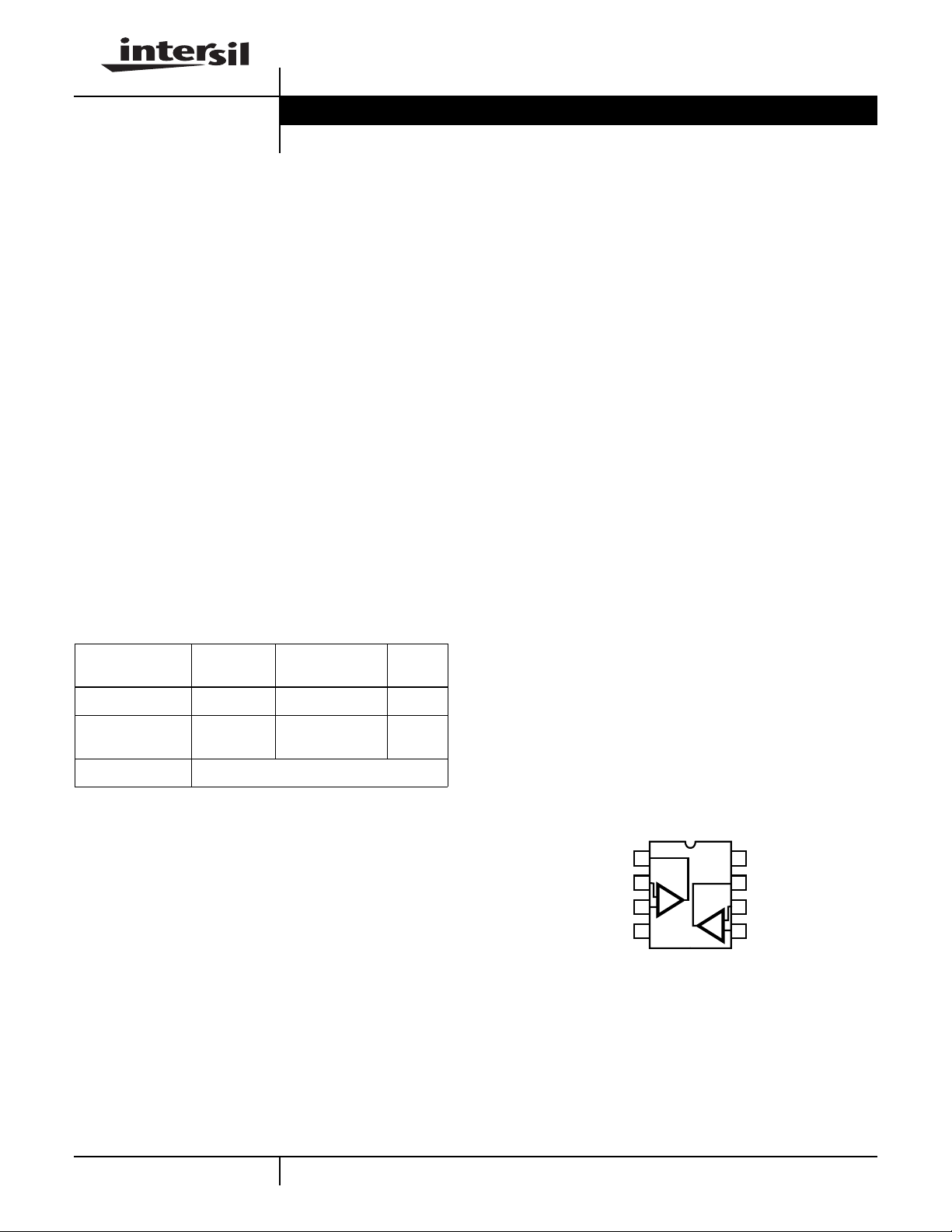
Pinout
HFA1205
(PDIP, SOIC)
TOP VIEW
OUT1
1
2
-IN1
+IN1
1
CAUTION: These devices are sensitive to electrostatic discharge; follow proper IC Handling Procedures.
http://www.intersil.com or 407-727-9207 | Copyright © Intersil Corporation 1999
-
+
3
4
V-
8
V+
7
OUT2
6
-IN2
-
+
5
+IN2

HFA1205
Absolute Maximum Ratings Thermal Information
Voltage Between V+ and V-. . . . . . . . . . . . . . . . . . . . . . . . . . . . .11V
DC Input Voltage . . . . . . . . . . . . . . . . . . . . . . . . . . . . . . . . V
Differential Input Voltage . . . . . . . . . . . . . . . . . . . . . . . . . . . . . . . .8V
Output Current (Note 2). . . . . . . . . . . . . . . . .Short Circuit Protected
30mA Continuous
60mA ≤ 50% Duty Cycle
ESD Rating
Human Body Model (Per MIL-STD-883 Method 3015.7). . . .600V
SUPPLY
Operating Conditions
Temperature Range. . . . . . . . . . . . . . . . . . . . . . . . . . -40oC to 85oC
CAUTION: Stresses above those listed in “Absolute Maximum Ratings” may cause permanent damage to the device. This is a stress only rating and operationofthe
device at these or any other conditions above those indicated in the operational sections of this specification is not implied.
NOTES:
1. θJA is measured with the component mounted on an evaluation PC board in free air.
2. Output is short circuit protected to ground. Brief short circuits to ground will not degrade reliability, however continuous (100% duty cycle) output
current must not exceed 30mA for maximum reliability.
Thermal Resistance (Typical, Note 1) θJA (oC/W)
PDIP Package . . . . . . . . . . . . . . . . . . . . . . . . . . . . . 130
SOIC Package . . . . . . . . . . . . . . . . . . . . . . . . . . . . . 160
Maximum Junction Temperature (Die Only) . . . . . . . . . . . . . . . .175oC
Maximum Junction Temperature (Plastic Package) . . . . . . . .150oC
Maximum Storage Temperature Range. . . . . . . . . . -65oC to 150oC
Maximum Lead Temperature (Soldering 10s) . . . . . . . . . . . . 300oC
(SOIC - Lead Tips Only)
Electrical Specifications V
PARAMETER TEST CONDITIONS
INPUT CHARACTERISTICS
Input Offset Voltage A 25 - 2 5 mV
Average Input Offset Voltage Drift B Full - 1 10 µV/oC
Input Offset Voltage
Common-Mode Rejection Ratio
Input Offset Voltage
Power Supply Rejection Ratio
Non-Inverting Input Bias Current A 25 - 6 15 µA
Non-Inverting Input Bias Current Drift B Full - 5 60 nA/oC
Non-Inverting Input Bias Current
Power Supply Sensitivity
Non-Inverting Input Resistance ∆VCM = ±1.8V A 25 0.8 2 - MΩ
Inverting Input Bias Current A 25 - 2 8.5 µA
Inverting Input Bias Current Drift B Full - 60 200 nA/oC
Inverting Input Bias Current
Common-Mode Sensitivity
= ±5V, AV = +1, RF = 560Ω, RL = 100Ω, Unless Otherwise Specified
SUPPLY
(NOTE 3)
TEST
LEVEL
A Full - 3 8 mV
∆VCM = ±1.8V A 25 45 48 - dB
∆VCM= ±1.8V A 85 43 46 - dB
∆VCM = ±1.2V A -40 43 46 - dB
∆VPS = ±1.8V A 25 48 52 - dB
∆VPS = ±1.8V A 85 46 50 - dB
∆VPS = ±1.2V A -40 46 50 - dB
A Full - 10 25 µA
∆VPS = ±1.8V A 25 - 0.5 1 µA/V
∆VPS = ±1.8V A 85 - 0.8 3 µA/V
∆VPS = ±1.2V A -40 - 0.8 3 µA/V
∆VCM = ±1.8V A 85 0.5 1.3 - MΩ
∆VCM = ±1.2V A -40 0.5 1.3 - MΩ
A Full - 5 15 µA
∆VCM = ±1.8V A 25 - 3 6 µA/V
∆VCM = ±1.8V A 85 - 4 8 µA/ V
∆VCM = ±1.2V A -40 - 4 8 µA/V
TEMP.
(oC) MIN TYP MAX UNITS
2

HFA1205
Electrical Specifications V
= ±5V, AV = +1, RF = 560Ω, RL = 100Ω, Unless Otherwise Specified (Continued)
SUPPLY
(NOTE 3)
PARAMETER TEST CONDITIONS
Inverting Input Bias Current
Power Supply Sensitivity
TEST
LEVEL
∆VPS = ±1.8V A 25 - 2 5 µA/V
∆VPS = ±1.8V A 85 - 4 8 µA/V
TEMP.
(oC) MIN TYP MAX UNITS
∆VPS = ±1.2V A -40 - 4 8 µA/V
Inverting Input Resistance C 25 - 60 - Ω
Input Capacitance C 25 - 1.6 - pF
Input Voltage Common Mode Range
(Implied by VIO CMRR, +RIN, and -I
tests)
BIAS
CMS
A 25, 85 ±1.8 ±2.4 - V
A -40 ±1.2 ±1.7 - V
Input Noise Voltage Density f = 100kHz B 25 - 3.5 - nV/√Hz
Non-Inverting Input Noise Current Density f = 100kHz B 25 - 2.5 - pA/√Hz
Inverting Input Noise Current Density f = 100kHz B 25 - 20 - pA/√Hz
TRANSFER CHARACTERISTICS
Open Loop Transimpedance Gain AV = -1 C 25 - 500 - kΩ
AC CHARACTERISTICS AV = +2, RF = 464Ω, Unless Otherwise Specified
-3dB Bandwidth (V
OUT
= 0.2V
)A
P-P
= +1, +RS= 432Ω B 25 - 280 - MHz
V
AV = +2 B 25 - 400 - MHz
AV = -1, RF= 332Ω B 25 - 360 - MHz
Full Power Bandwidth
(V
=5V
at AV= +2/-1,
P-P
at AV = +1)
4V
OUT
P-P
AV = +1, RS= 432Ω B 25 - 140 - MHz
AV = +2 B 25 - 125 - MHz
AV = -1, RF= 332Ω B 25 - 180 - MHz
Gain Flatness (AV = +2,V
OUT
= 0.2V
) To 25MHz B 25 - ±0.02 - dB
P-P
To 50MHz B 25 - ±0.03 - dB
Minimum Stable Gain A Full - 1 - V/V
Crosstalk 5MHz B 25 - -60 - dB
10MHz B 25 - -54 - dB
OUTPUT CHARACTERISTICS RF = 560Ω, Unless Otherwise Specified
Output Voltage Swing AV= -1, RL= 100Ω A25±3 ±3.4 - V
A Full ±2.8 ±3- V
Output Current AV = -1, RL = 50Ω A 25, 85 50 60 - mA
A -40 28 42 - mA
Output Short Circuit Current B 25 - 90 - mA
Closed Loop Output Impedance DC, AV = +2, RF = 464Ω B 25 - 0.07 - Ω
Second Harmonic Distortion
(AV= +2, RF= 464Ω, V
OUT
Third Harmonic Distortion
(AV= +2, RF= 464Ω, V
OUT
=2V
=2V
P-P
P-P
)
)
10MHz B 25 - -50 - dBc
20MHz B 25 - -45 - dBc
10MHz B 25 - -55 - dBc
20MHz B 25 - -50 - dBc
TRANSIENT CHARACTERISTICS AV = +2, RF = 464Ω, Unless Otherwise Specified
Rise and Fall Times (V
OUT
= 0.5V
) Rise Time B 25 - 0.8 - ns
P-P
Fall Time B 25 - 1.25 - ns
3
 Loading...