Intersil Corporation HFA1120, HFA1100 Datasheet

HFA1100, HFA1120
Data Sheet May 1999 File Number
850MHz, Low Distortion Current Feedback
Operational Amplifiers
The HFA1100, 1120 are a family of high-speed, wideband,
fast settling current feedback amplifiers built with Intersil's
proprietary complementary bipolar UHF-1 process. Both
amplifiers operatewith single supply voltages as low as 4.5V
(see Application Information section).
The HFA1100 is a basic op amp with uncommitted pins 1, 5,
and 8. The HFA1120 includes inverting input bias current
adjust pins (pins 1 and 5) for adjusting the output offset
voltage.
These devices offer a significant performance improvement
over the AD811, AD9617/18, the CLC400-409, and the
EL2070, EL2073, EL2030.
For Military grade product refer to the HFA1100/883,
HFA1120/883 data sheet.
Ordering Information
PART NUMBER
(BRAND)
HFA1100IP -40 to 85 8 Ld PDIP E8.3
HFA1100IB
(H1100I)
HFA1120IB
(H1120I)
HFA11XXEVAL DIPEvaluationBoard for High-Speed Op Amps
TEMP.
RANGE (oC) PACKAGE PKG. NO.
-40 to 85 8 Ld SOIC M8.15
-40 to 85 8 Ld SOIC M8.15
The Op Amps with Fastest Edges
0ns 25ns
Features
• Low Distortion (30MHz, HD2). . . . . . . . . . . . . . . . . -56dBc
• -3dB Bandwidth . . . . . . . . . . . . . . . . . . . . . . . . . . 850MHz
• Very Fast Slew Rate. . . . . . . . . . . . . . . . . . . . . . 2300V/µs
• Fast Settling Time (0.1%). . . . . . . . . . . . . . . . . . . . . 11ns
• Excellent Gain Flatness
- (100MHz) . . . . . . . . . . . . . . . . . . . . . . . . . . . . . ±0.14dB
- (50MHz) . . . . . . . . . . . . . . . . . . . . . . . . . . . . . . ±0.04dB
• High Output Current. . . . . . . . . . . . . . . . . . . . . . . . . 60mA
• Overdrive Recovery . . . . . . . . . . . . . . . . . . . . . . . . <10ns
• Operates with 5V Single Supply (See AN9745)
Applications
• Video Switching and Routing
• Pulse and Video Amplifiers
• RF/IF Signal Processing
• Flash A/D Driver
• Medical Imaging Systems
• Related Literature
- AN9420, Current Feedback Theory
- AN9202, HFA11XX Evaluation Fixture
- AN9745, Single 5V Supply Operation
Pinouts
HFA1100
(PDIP, SOIC)
TOP VIEW
INPUT
220MHz
SIGNAL
OUTPUT
= 2)
(A
V
HFA1130
OP AMP
NC
-IN
+IN
V-
1
2
3
4
TOP VIEW
-
+
HFA1120
(SOIC)
8
NC
V+
7
OUT
6
NC
5
2945.7
BAL
1
-IN
2
-
+IN
V-
1
CAUTION: These devices are sensitive to electrostatic discharge; follow proper IC Handling Procedures.
http://www.intersil.com or 407-727-9207 | Copyright © Intersil Corporation 1999
+
3
4
NC
8
V+
7
OUT
6
BAL
5

HFA1100, HFA1120
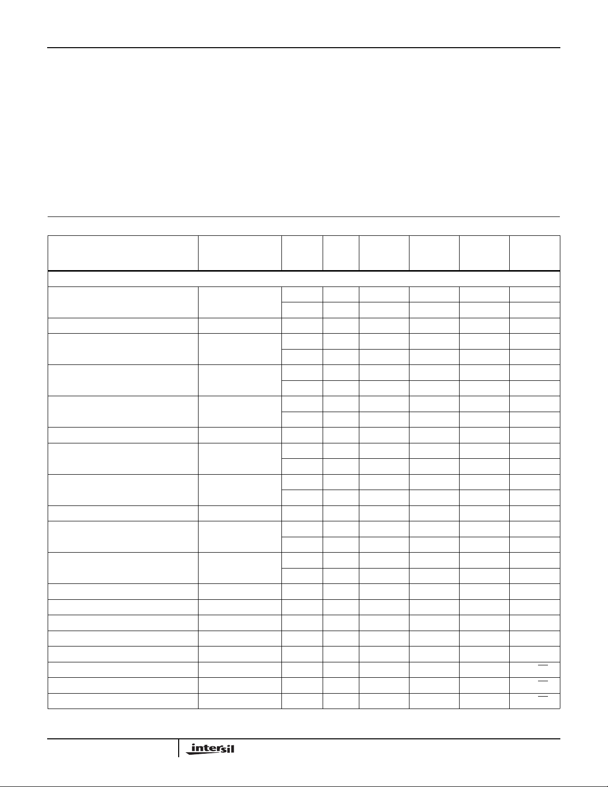
Absolute Maximum Ratings T
Voltage Between V+ and V-. . . . . . . . . . . . . . . . . . . . . . . . . . . . 12V
Input Voltage . . . . . . . . . . . . . . . . . . . . . . . . . . . . . . . . . . . V
Differential Input Voltage . . . . . . . . . . . . . . . . . . . . . . . . . . . . . . . 5V
Output Current (50% Duty Cycle) . . . . . . . . . . . . . . . . . . . . . . 60mA
Operating Conditions
Temperature Range. . . . . . . . . . . . . . . . . . . . . . . . . . -40oC to 85oC
CAUTION: Stresses above those listed in “Absolute Maximum Ratings” may cause permanent damage to the device. This is a stress only rating and operationofthe
device at these or any other conditions above those indicated in the operational sections of this specification is not implied.
NOTE:
1. θJA is measured with the component mounted on an evaluation PC board in free air.
Electrical Specifications V
PARAMETER
INPUT CHARACTERISTICS
Input Offset Voltage (Note 3) A 25 - 2 6 mV
Input Offset Voltage Drift C Full - 10 - µV/oC
CMRR ∆VCM = ±2V A 25 40 46 - dB
V
IO
PSRR ∆VS = ±1.25V A 25 45 50 - dB
V
IO
Non-Inverting Input Bias Current
(Note 3)
Drift C Full - 40 - nA/oC
+I
BIAS
CMS ∆VCM = ±2V A 25 - 20 40 µA/V
+I
BIAS
Inverting Input Bias Current (Note 3) -IN = 0V A 25 - 12 50 µA
Drift C Full - 40 - nA/oC
-I
BIAS
CMS ∆VCM = ±2V A 25 - 1 7 µA/V
-I
BIAS
-I
PSS ∆VS = ±1.25V A 25 - 6 15 µA/V
BIAS
Adj. Range (HFA1120) A 25 ±100 ±200 - µA
-I
BIAS
Non-Inverting Input Resistance A 25 25 50 - kΩ
Inverting Input Resistance C 25 - 20 30 Ω
Input Capacitance (Either Input) B 25 - 2 - pF
Input Common Mode Range C Full ±2.5 ±3.0 - V
Input Noise Voltage (Note 3) 100kHz B 25 - 4 - nV/√
+Input Noise Current (Note 3) 100kHz B 25 - 18 - pA/√
-Input Noise Current (Note 3) 100kHz B 25 - 21 - pA/√
= 25oC Thermal Information
A
Thermal Resistance (Typical, Note 1) θJA (oC/W) θJC (oC/W)
SUPPLY
= ±5V, AV = +1, RF = 510Ω, RL = 100Ω, Unless Otherwise Specified
SUPPLY
(NOTE 2)
TEST
CONDITIONS
+IN = 0V A 25 - 25 40 µA
TEST
LEVEL
A Full - - 10 mV
A Full 38 - - dB
A Full 42 - - dB
A Full - - 65 µA
A Full - - 50 µA/V
A Full - - 60 µA
A Full - - 10 µA/V
A Full - - 27 µA/V
PDIP Package . . . . . . . . . . . . . . . . . . . 130 N/A
SOIC Package . . . . . . . . . . . . . . . . . . . 170 N/A
Maximum Junction Temperature (Plastic Package). . . . . . . . .150oC
Maximum Storage Temperature Range. . . . . . . . . . -65oC to 150oC
Maximum Lead Temperature (Soldering 10s) . . . . . . . . . . . . 300oC
(SOIC - Lead Tips Only)
TEMP.
o
C) MIN TYP MAX UNITS
(
Hz
Hz
Hz
2

HFA1100, HFA1120
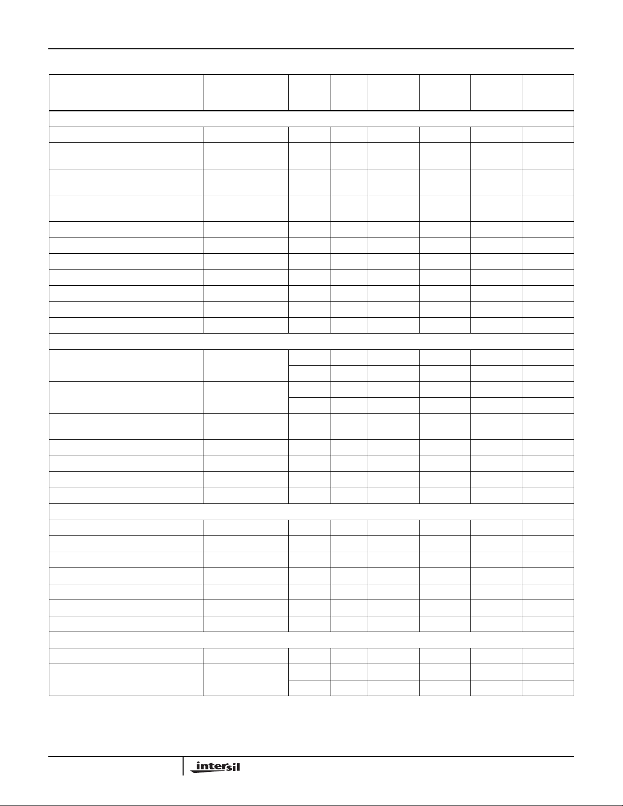
Electrical Specifications V
= ±5V, AV = +1, RF = 510Ω, RL = 100Ω, Unless Otherwise Specified (Continued)
SUPPLY
(NOTE 2)
PARAMETER
TEST
CONDITIONS
TEST
LEVEL
TEMP.
o
C) MIN TYP MAX UNITS
(
TRANSFER CHARACTERISTICS AV = +2, Unless Otherwise Specified
Open Loop Transimpedance (Note 3) B 25 - 300 - kΩ
-3dB Bandwidth (Note 3) V
OUT
= 0.2V
P-P
,
B 25 530 850 - MHz
AV = +1
-3dB Bandwidth V
OUT
= 0.2V
P-P
,
B 25 - 670 - MHz
AV = +2, RF = 360Ω
Full Power Bandwidth V
OUT
= 4V
P-P
,
B 25 - 300 - MHz
AV = -1
Gain Flatness (Note 3) To 100MHz B 25 - ±0.14 - dB
Gain Flatness To 50MHz B 25 - ±0.04 - dB
Gain Flatness To 30MHz B 25 - ±0.01 - dB
Linear Phase Deviation (Note 3) DC to 100MHz B 25 - 0.6 - Degrees
Differential Gain NTSC, R
Differential Phase NTSC, R
= 75Ω B 25 - 0.03 - %
L
= 75Ω B 25 - 0.05 - Degrees
L
Minimum Stable Gain A Full 1 - - V/V
OUTPUT CHARACTERISTICS A
Output Voltage (Note 3) A
= +2, Unless Otherwise Specified
V
= -1 A 25 ±3.0 ±3.3 - V
V
A Full ±2.5 ±3.0 - V
Output Current R
= 50Ω, AV = -1 A 25, 85 50 60 - mA
L
A -40 35 50 - mA
DC Closed Loop Output Impedance
B 25 - 0.07 - Ω
(Note 3)
2nd Harmonic Distortion (Note 3) 30MHz, V
3rd Harmonic Distortion (Note 3) 30MHz, V
OUT
OUT
= 2V
= 2V
P-P
P-P
B 25 - -56 - dBc
B 25 - -80 - dBc
3rd Order Intercept (Note 3) 100MHz B 25 20 30 - dBm
1dB Compression 100MHz B 25 15 20 - dBm
TRANSIENT RESPONSE A
Rise Time V
Overshoot (Note 3) V
Slew Rate A
Slew Rate A
0.1% Settling (Note 3) V
0.2% Settling (Note 3) V
= +2, Unless Otherwise Specified
V
= 2.0V Step B 25 - 900 - ps
OUT
= 2.0V Step B 25 - 10 - %
OUT
= +1, V
V
= +2, V
V
= 2V to 0V B 25 - 11 - ns
OUT
= 2V to 0V B 25 - 7 - ns
OUT
OUT
OUT
=5V
=5V
P-P
P-P
B 25 - 1400 - V/µs
B 25 1850 2300 - V/µs
Overdrive Recovery Time 2X Overdrive B 25 - 7.5 10 ns
POWER SUPPLY CHARACTERISTICS
Supply Voltage Range B Full ±4.5 - ±5.5 V
Supply Current (Note 3) A 25 - 21 26 mA
A Full - - 33 mA
NOTES:
2. Test Level: A. Production Tested; B. Typical or Guaranteed Limit Based on Characterization; C. Design Typical for Information Only.
3. See Typical Performance Curves for more information.
3
 Loading...