Intersil Corporation HFA1115 Datasheet
HFA1115
September 1998 File Number 3606.4
225MHz, Low Power, Output
Limiting, Closed Loop Buffer Amplifier
The HF A1115isahighspeedclosedloopBuffer featuring both
user programmable gain and output limiting. Manuf actured on
Intersil’sproprietary complementary bipolarUHF-1 process,the
HF A1115 also off ers a wide -3dB bandwidth of 225MHz, v ery
fast slew rate , e xcellent gain flatness and high output current.
This buffer is the ideal choice f or high frequency applications
requiring output limiting, especially those needing ultra fast
overload recovery times. The limiting function allows the
designer to set the maximum positive and negative output
levels, thereby protecting later stages from damage or input
saturation. The HFA1115 also allows for v oltage gains of +2,
+1, and -1, without the use of external resistors. Gain
selection is accomplished via connections to the inputs, as
described in the “Application Information” text. The result is a
more flexible product, f ewer part types in inventory, and more
efficient use of board space.
Compatibility with existing op amp pinouts provides flexibility
to upgrade low gain amplifiers, while decreasing component
count. Unlike most buffers , the standard pinout provides an
upgrade path, should a higher closed loop gain be needed at
a future date. For Military product, refer to the HFA1115/883
data sheet.
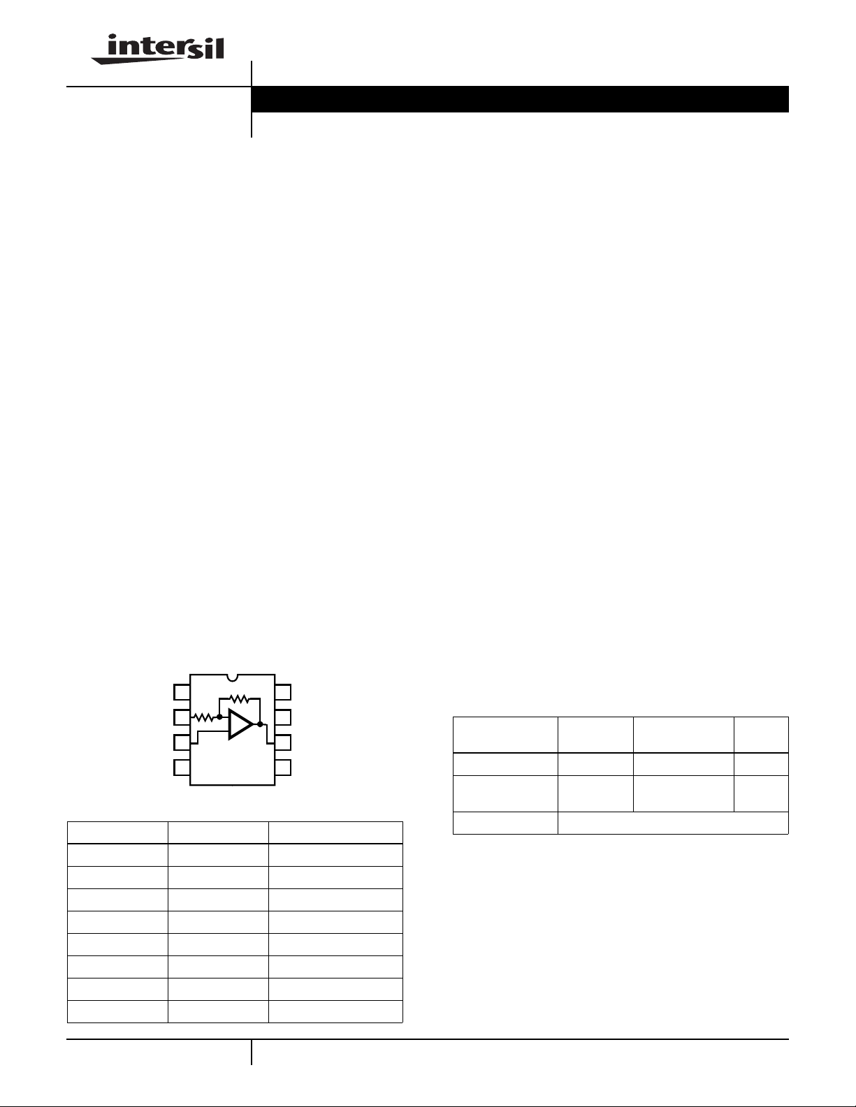
Pinout
HFA1115
(PDIP, SOIC)
TOP VIEW
350
350
_
+
8
V
H
7
V+
OUT
6
V
5
L
NC
-IN
+IN
1
2
3
V-
4
Pin Descriptions
NAME PIN NUMBER DESCRIPTION
NC 1 No Connection
-IN 2 Inverting Input
+IN 3 Non-Inverting Input
V- 4 Negative Supply
V
L
OUT 6 Output
V+ 7 Positive Supply
V
H
5 Lower Output Limit
8 Upper Output Limit
Features
• User Programmable Output Voltage Limiting
• High Input Impedance . . . . . . . . . . . . . . . . . . . . . . . 1MΩ
• Differential Gain . . . . . . . . . . . . . . . . . . . . . . . . . . . 0.02%
• Differential Phase. . . . . . . . . . . . . . . . . . . . 0.03 Degrees
• Wide -3dB Bandwidth (A
• Very Fast Slew Rate (A
= +2). . . . . . . . . . . . . .225MHz
V
= -1) . . . . . . . . . . . . . . 1135V/µs
V
• Low Supply Current . . . . . . . . . . . . . . . . . . . . . . . . 7.1mA
• High Output Current. . . . . . . . . . . . . . . . . . . . . . . . .60mA
• Excellent Gain Accuracy . . . . . . . . . . . . . . . . . . . 0.99V/V
• User Programmable For Closed-Loop Gains of +1, -1 or
+2 Without Use of External Resistors
• Fast Overdrive Recovery . . . . . . . . . . . . . . . . . . . . . <1ns
• Standard Operational Amplifier Pinout
Applications
• Flash A/D Drivers
• Video Cable Drivers
• High Resolution Monitors
• Professional Video Processing
• Medical Imaging
• Video Digitizing Boards/Systems
• Battery Powered Communications
Ordering Information
PART NUMBER
(BRAND)
HFA1115IP -40 to 85 8 Ld PDIP E8.3
HFA1115IB
(H1115I)
HFA11XXEVAL High Speed Op Amp DIP Evaluation Board
TEMP.
RANGE (oC) PACKAGE
-40 to 85 8 Ld SOIC M8.15
PKG.
NO.
1
CAUTION: These devices are sensitive to electrostatic discharge; follow proper IC Handling Procedures.
http://www.intersil.com or 407-727-9207 | Copyright © Intersil Corporation 1999
HFA1115
Absolute Maximum Ratings Thermal Information
Voltage Between V+ and V-. . . . . . . . . . . . . . . . . . . . . . . . . . . . 11V
DC Input Voltage . . . . . . . . . . . . . . . . . . . . . . . . . . . . . . . . V
Output Current (Note 2). . . . . . . . . . . . . . . . Short Circuit Protected
ESD Rating
Human Body Model (Per MIL-STD-883 Method 3015.7). . . .600V
SUPPLY
Operating Conditions
Temperature Range. . . . . . . . . . . . . . . . . . . . . . . . . . -40oC to 85oC
Supply Voltage Range (Typical). . . . . . . . . . . . . . . . . . . . 5V to 10V
CAUTION: Stresses above those listed in “Absolute Maximum Ratings” may cause permanent damage to the device. This is a stress only rating and operationofthe
device at these or any other conditions above those indicated in the operational sections of this specification is not implied.
NOTES:
1. θJA is measured with the component mounted on an evaluation PC board in free air.
2. Output is protected for short circuits to ground. Brief short circuits to ground will not degrade reliability, however,continuous (100% duty cycle)
output current should not exceed 30mA for maximum reliability.
Thermal Resistance (Typical, Note 1) θJA (oC/W)
PDIP Package . . . . . . . . . . . . . . . . . . . . . . . . . . . . . 130
SOIC Package . . . . . . . . . . . . . . . . . . . . . . . . . . . . . 170
Maximum Junction Temperature (Die) . . . . . . . . . . . . . . . . . . . .175oC
Maximum Junction Temperature (Plastic Packages) . . . . . . .150oC
Maximum Storage Temperature Range. . . . . . . . . . -65oC to 150oC
Maximum Lead Temperature (Soldering 10s) . . . . . . . . . . . . 300oC
(SOIC - Lead Tips Only)
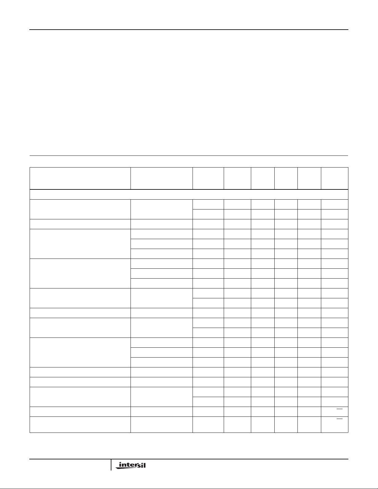
Electrical Specifications V
PARAMETER
INPUT CHARACTERISTICS
Output Offset Voltage A 25 - 2 10 mV
Average Output Offset Voltage Drift B Full - 22 70 µV/oC
Common-Mode Rejection Ratio ∆VCM = ±1.8V A 25 42 45 - dB
Power Supply Rejection Ratio ∆VPS = ±1.8V A 25 45 49 - dB
Non-Inverting Input Bias Current A 25 - 1 15 µA
Non-Inverting Input Bias Current Drift B Full - 30 80 nA/oC
Non-Inverting Input Bias Current Power
Supply Sensitivity
Non-Inverting Input Resistance ∆VCM = ±1.8V A 25 0.8 1.1 - MΩ
Inverting Input Resistance C 25 280 350 420 Ω
Input Capacitance C 25 - 1.6 - pF
Input Voltage Common Mode Range
(Implied by VIO CMRR and +RIN Tests)
Input Noise Voltage Density (Note 4) f = 100kHz B 25 - 7 - nV/√Hz
Non-Inverting Input Noise Current Density
(Note 4)
= ±5V, AV = +1, RL = 100Ω, Unless Otherwise Specified
SUPPLY
(NOTE 3)
TEST
CONDITIONS
∆VCM = ±1.8V A 85 40 44 - dB
∆VCM = ±1.2V A -40 40 45 - dB
∆VPS = ±1.8V A 85 43 48 - dB
∆VPS = ±1.2V A -40 43 48 - dB
∆VPS = ±1.25V A 25 - 0.5 1 µA/V
∆VCM = ±1.8V A 85 0.5 1.4 - MΩ
∆VCM = ±1.2V A -40 0.5 1.3 - MΩ
f = 100kHz B 25 - 3.6 - pA/√Hz
TEST
LEVEL
A Full - 3 15 mV
A Full - 3 25 µA
A Full - - 3 µA/V
A 25, 85 ±1.8 ±2.4 - V
A -40 ±1.2 ±1.7 - V
TEMP.
(oC) MIN TYP MAX UNITS
2
HFA1115
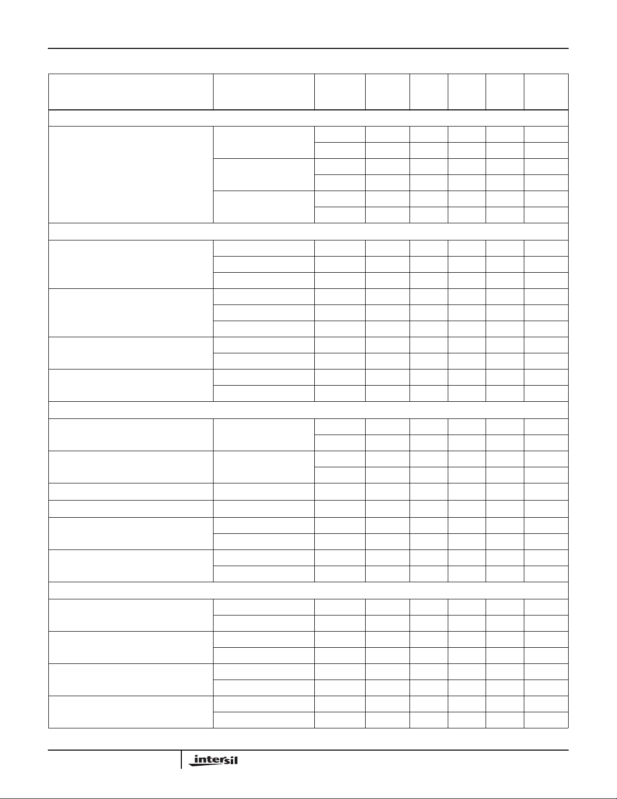
Electrical Specifications V
= ±5V, AV = +1, RL = 100Ω, Unless Otherwise Specified (Continued)
SUPPLY
(NOTE 3)
PARAMETER
TEST
CONDITIONS
TEST
LEVEL
TEMP.
(oC) MIN TYP MAX UNITS
TRANSFER CHARACTERISTICS
Gain AV = -1 A 25 -0.98 -0.996 -1.02 V/V
A Full -0.975 -1.000 -1.025 V/V
AV = +1 A 25 0.98 0.992 1.02 V/V
A Full 0.975 0.993 1.025 V/V
AV = +2 A 25 1.96 1.988 2.04 V/V
A Full 1.95 1.990 2.05 V/V
AC CHARACTERISTICS
-3dB Bandwidth
(V
= 0.2V
OUT
P-P
, Note 4)
AV = -1 B 25 - 225 - MHz
AV = +1, +RS = 620Ω B 25 - 200 - MHz
AV = +2 B 25 - 225 - MHz
Full Power Bandwidth
(V
= 5V
OUT
4V
at AV = +1, Note 4)
P-P
at AV = +2/-1,
P-P
AV = -1 B 25 - 157 - MHz
AV = +1, +RS = 620Ω B 25 - 140 - MHz
AV = +2 B 25 - 125 - MHz
Gain Flatness
(to 25MHz, V
Gain Flatness
(to 50MHz, V
OUT
OUT
= 0.2V
= 0.2V
P-P
P-P
, Note 4)
, Note 4)
AV = +1, +RS = 620Ω B25-±0.1 - dB
AV = +2 B 25 - ±0.04 - dB
AV = +1, +RS = 620Ω B25-±0.25 - dB
AV = +2 B 25 - ±0.1 - dB
OUTPUT CHARACTERISTICS
Output Voltage Swing (Note 4) AV = -1, RL = 100Ω A25±3.0 ±3.2 - V
A Full ±2.8 ±3.0 - V
Output Current (Note 4) AV = -1, RL = 50Ω A 25, 85 50 55 - mA
A -40 28 42 - mA
Output Short Circuit Current B 25 - 90 - mA
Output Resistance (Note 4) DC, AV = +2 B 25 - 0.07 - Ω
Second Harmonic Distortion
(AV = +2, V
OUT
= 2V
P-P
)
Third Harmonic Distortion
(AV = +2, V
OUT
= 2V
P-P
)
10MHz B 25 - -50 - dBc
20MHz B 25 - -45 - dBc
10MHz B 25 - -50 - dBc
20MHz B 25 - -45 - dBc
TRANSIENT RESPONSE AV = +2, Unless Otherwise Specified
Rise and Fall Times
(V
OUT
= 0.5V
P-P
, Note 4)
Overshoot
(V
OUT
= 0.5V
P-P
, VIN t
Slew Rate
(V
OUT
= 5V
, AV = -1)
P-P
Slew Rate
(V
OUT
= 4V
, AV = +1, +RS = 620Ω)
P-P
RISE
= 2.5ns)
Rise Time B 25 - 1.7 - ns
Fall Time B 25 - 1.9 - ns
+OS B 25 - 0 - %
-OS B 25 - 0 - %
+SR B 25 - 1660 - V/µs
-SR (Note 5) B 25 - 1135 - V/µs
+SR B 25 - 1125 - V/µs
-SR (Note 5) B 25 - 800 - V/µs
3
HFA1115
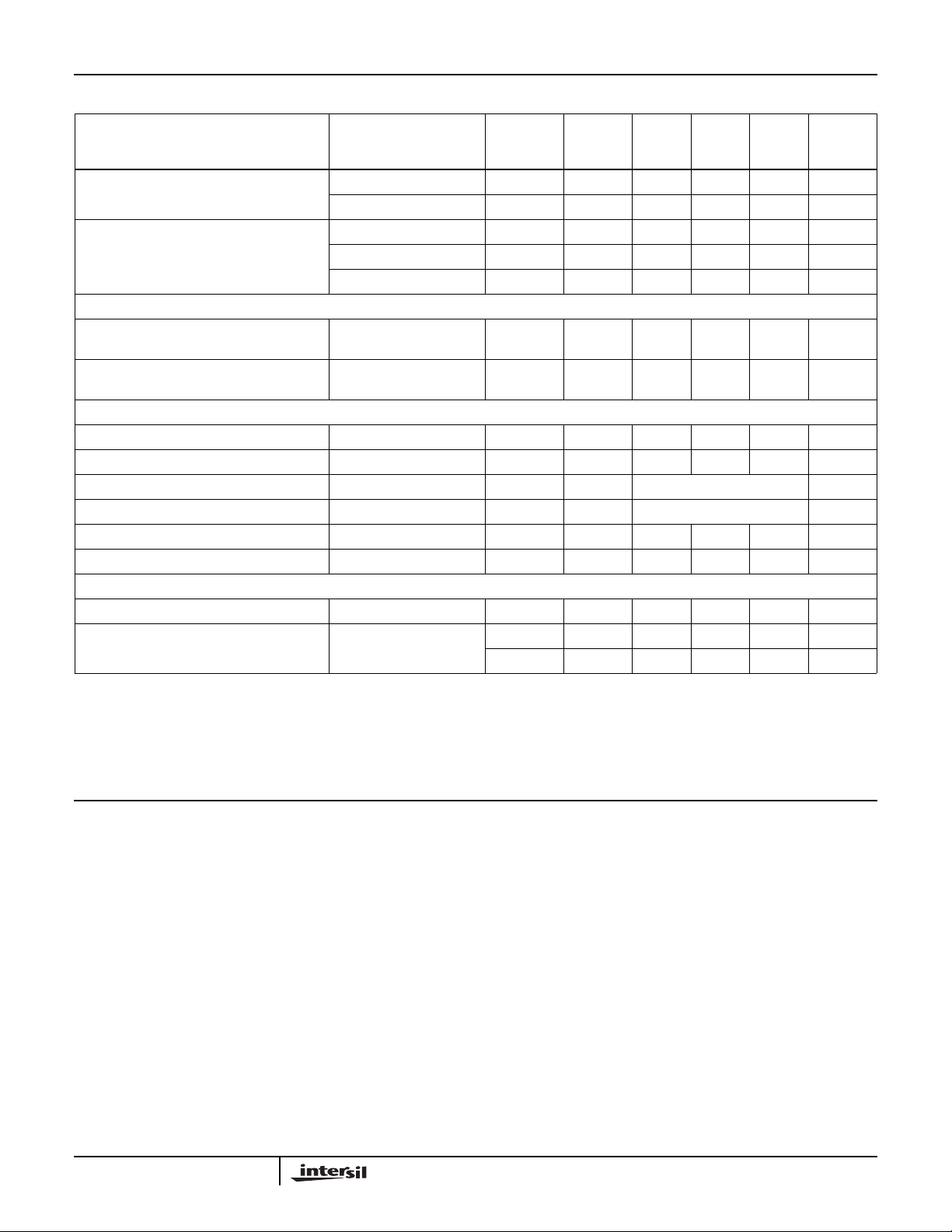
Electrical Specifications V
PARAMETER
Slew Rate
(V
= 5V
OUT
Settling Time
(V
= +2V to 0V step, Note 4)
OUT
VIDEO CHARACTERISTICS
Differential Gain f = 3.58MHz, AV = +2,
Differential Phase f = 3.58MHz, AV = +2,
OUTPUT LIMITING CHARACTERISTICS AV = +2, VH = +1V, VL = -1V, Unless Otherwise Specified
Limit Accuracy (Note 4) VIN = ±1.6V, AV = -1 A Full -125 -70 125 mV
Overdrive Recovery Time (Note 4) VIN = ±1V B 25 - 0.8 - ns
Negative Limit Range B 25 -5.0 to +2.5 V
Positive Limit Range B 25 -2.5 to +5.0 V
Limit Input Bias Current A Full - 85 200 µA
Limit Input Bandwidth C 25 - 100 - MHz
POWER SUPPLY CHARACTERISTICS
Power Supply Range C 25 4.5 - 5.5 ±V
Power Supply Current (Note 4) A 25 6.6 6.9 7.1 mA
NOTE:
3. Test Level: A. Production Tested; B. Typical or Guaranteed Limit Based on Characterization; C. Design Typical for Information Only.
4. See Typical Performance Curves for more information.
5. Slew rates are asymmetrical if the output swings below GND (e.g., a bipolar signal). Positive unipolar output signals have symmetric positive and
negative slew rates comparable to the +SR specification. See the “Application Information” section, and the pulse response graphs for details.
, AV = +2)
P-P
= ±5V, AV = +1, RL = 100Ω, Unless Otherwise Specified (Continued)
SUPPLY
(NOTE 3)
TEST
CONDITIONS
+SR B 25 - 1265 - V/µs
-SR (Note 5) B 25 - 870 - V/µs
To 0.1% B 25 - 23 - ns
To 0.05% B 25 - 33 - ns
To 0.02% B 25 - 45 - ns
RL = 150Ω
RL = 150Ω
TEST
LEVEL
B 25 - 0.02 - %
B 25 - 0.03 - Degrees
A Full - 7.1 7.3 mA
TEMP.
(oC) MIN TYP MAX UNITS
Application Information
Relevant Application Notes
The following Application Notes pertain to the HFA1115:
• AN9653-Use and Application of Output Limiting
Amplifiers
• AN9752-Sync Stripper and Sync Inserter for
Composite Video
These publications may be obtained from Intersil’s web site
(http://www.intersil.com) or via our AnswerFax system.
HFA1115 Advantages
The HFA1115 features a novel design which allows the user
to select from three closed loop gains, without any external
components. The result is a more flexible product, fewerpart
types in inventory, and more efficient use of board space.
Implementing a gain of 2, cable driver with this IC eliminates
4
the two gain setting resistors, which frees up board space for
termination resistors.
Like most newer high performance amplifiers, the HFA1115
is a current feedback amplifier (CFA). CFAs offer high
bandwidth and slew rate at low supply currents, but can be
difficult to use because of their sensitivity to feedback
capacitance and parasitics on the inverting input (summing
node). The HFA1115 eliminates these concerns by bringing
the gain setting resistors on-chip. This yields the optimum
placement and value of the feedback resistor, while
minimizing feedbackand summing node parasitics. Because
there is no access to the summing node, the PCB parasitics
do not impact performance at gains of +2 or -1 (see “Unity
Gain Considerations” for discussion of parasitic impact on
unity gain performance).
HFA1115
The HFA1115’s closed loop gain implementation provides
better gain accuracy, lower offset and output impedance,
and better distortion compared with open loop buffers.
Closed Loop Gain Selection
This “buffer” operates in closed loop gains of -1, +1, or +2, and
gain selection is accomplished via connections to the ±inputs.
Applying the input signal to +IN and floating -IN selects a gain
of +1 (see next section for la y out ca v eats), while g rounding -IN
selects a gain of +2. A gain of -1 is obtained by applying the
input signal to -IN with +IN grounded through a 50Ω resistor.
The table below summarizes these connections:
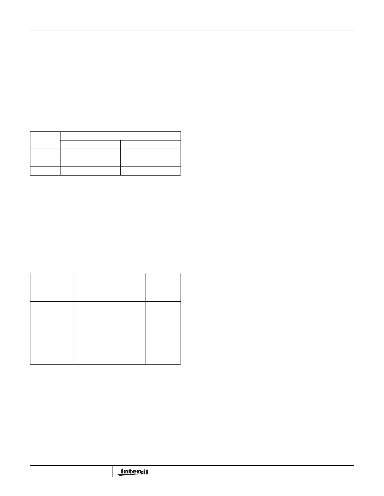
GAIN
(AV)
-1 50Ω to GND Input
+1 Input NC (Floating)
+2 Input GND
+INPUT (PIN 3) -INPUT (PIN 2)
CONNECTIONS
Unity Gain Considerations
Unity gain selection is accomplished by floating the -Input of
the HFA1115. Anything that tends to short the -Input to GND,
such as straycapacitance at high frequencies, will cause the
amplifier gain to increase toward a gain of +2. The result is
excessive high frequency peaking, and possible instability.
Even the minimal amount of capacitance associated with
attaching the -Input lead to the PCB results in approximately
3dB of gain peaking. At a minimum this requires due care to
ensure the minimum capacitance at the -Input connection.
TABLE 1. UNITY GAIN PERFORMANCE FOR VARIOUS
IMPLEMENTATIONS
±0.1dB
PEAK-
ING
APPROACH
Remove Pin 2 2.5 400 1200/850 20
+RS = 620Ω 0.6 170 1125/800 25
+RS = 620Ω and
Remove Pin 2
Short Pins 2, 3 0 200 875/550 45
100pF cap. be-
tween pins 2, 3
(dB)BW(MHz)
0 165 1050/775 65
0.2 190 900/550 19
+SR/-SR
(V/µs)
Table 1 lists five alternate methods for configuring the
HFA1115 as a unity gain buffer, and the corresponding
performance. The implementations vary in complexity and
involve performance trade-offs. The easiest approach to
implement is simply shorting the two input pins together,and
applying the input signal to this common node. The amplifier
bandwidth drops from 400MHz to 200MHz, but excellent
gain flatness is the benefit. Another drawback to this
approach is that the amplifier input noise voltage and input
offset voltage terms see a gain of +2, resulting in higher
noise and output offset voltages. Alternately, a 100pF
capacitor between the inputs shorts them only at high
GAIN
FLATNESS
(MHz)
frequencies, which prevents the increased output offset
voltage but delivers less gain flatness.
Another straightforward approach is to add a 620Ω resistor
in series with the positive input. This resistor and the
HFA1115 input capacitance form a low pass filter which rolls
off the signal bandwidth before gain peaking occurs. This
configuration was employed to obtain the datasheet AC and
transient parameters for a gain of +1.
Non-inverting Input Source Impedance
For best operation, the DC source impedance seen by the
non-inverting input should be ≥50Ω. This is especially
important in inverting gain configurations where the noninverting input would normallybe connected directly to GND.
Pulse Undershoot and Asymmetrical Slew Rates
The HFA1115utilizes a quasi-complementaryoutput stage to
achievehigh output current while minimizing quiescent supply
current. In this approach, a composite device replaces the
traditional PNP pulldown transistor. The composite device
switches modes after crossing 0V, resulting in added
distortion for signals swinging below ground, and an
increased undershoot on the negative portion of the output
waveform (see Figures 9, 13, and 17). This undershoot isn’t
present for small bipolar signals, or large positive signals.
Another artifact of the composite device is asymmetrical slew
rates for output signals with a negative voltage component.
The slew rate degrades as the output signal crosses through
.
0V (see Figures 9, 13, and 17), resulting in a slower overall
negative slew rate. Positive only signals have symmetrical
slew rates as illustrated in the large signal positive pulse
response graphs (see Figures 7, 11, and 15).
PC Board Layout
This amplifier’s frequency response depends greatly on the
care taken in designing the PC board. The use of low
inductance components such as chip resistors and chip
capacitors is strongly recommended, while a solid
ground plane is a must!
Attention should be given to decoupling the power supplies.
A large value (10µF) tantalum in parallel with a small value
(0.1µF) chip capacitor works well in most cases.
Terminatedmicrostrip signal lines are recommended at the input
and output of the device. Capacitance directly on the output
must be minimized, or isolated as discussed in the next section.
For unity gain applications, care must also be taken to
minimize the capacitance to ground at the amplifier’s
inverting input. At higher frequencies this capacitance tends
to short the -INPUT to GND, resulting in a closed loop gain
which increases with frequency. This causes excessive high
frequency peaking and potentially other problems as well.
An example of a good high frequency layout is the
Evaluation Board shown in Figure 2.
5
 Loading...