

Page 1

HFA1113
Data Sheet February 1999 File Number 1342.5
850MHz, Low Distortion, Output Limiting,
Programmable Gain, Buffer Amplifier
The HFA1113 is a high speed Buffer featuring user
programmable gain and output limiting coupled with ultra
high speed performance. This buffer is the ideal choice for
high frequency applications requiring output limiting,
especially those needing ultra fast overload recovery times.
The output limiting function allows the designer to set the
maximum positive and negative output levels, thereby
protecting later stages from damage or input saturation. The
sub-nanosecond overdrive recovery time quickly returns the
amplifier to linear operation following an overdrive condition.
A unique feature of the pinout allows the user to select a
voltage gain of +1, -1, or +2, without the use of any external
components, as described in the “Application Information”
section. Compatibility with existing op amp pinouts provides
flexibility to upgrade low gain amplifiers, while decreasing
component count. Unlike most buffers, the standard pinout
provides an upgrade path should a higher closed loop gain
be needed at a future date.
Component and composite video systems will also benefit
from this buffer’s performance, as indicated by the excellent
gain flatness, and 0.02%/0.04 Degree Differential
Gain/Phase specifications (R
= 150Ω).
L
For Military product, refer to the HFA1113/883 data sheet.
Ordering Information
PART NUMBER
(BRAND)
HFA1113IB
(H1113I)
HFA11XXEVAL DIPEvaluation Board For High Speed Op Amps
TEMP.
RANGE (oC) PACKAGE
-40 to 85 8 Ld SOIC M8.15
PKG.
NO.
Pinout
HFA1113
(SOIC)
TOP VIEW
NC
-IN
+IN
1
2
3
V-
4
300
300
-
+
8
V
H
7
V+
OUT
6
V
5
L
Features
• User Programmable Output Voltage Limiting
• User Programmable For Closed-Loop Gains of +1, -1 or
+2 Without Use of External Resistors
• Wide -3dB Bandwidth. . . . . . . . . . . . . . . . . . . . . .850MHz
• Excellent Gain Flatness (to 100MHz). . . . . . . . . . ±0.07dB
• Low Differential Gain and Phase . . . 0.02%/0.04 Degrees
• Low Distortion (HD3, 30MHz). . . . . . . . . . . . . . . . . -73dBc
• Very Fast Slew Rate . . . . . . . . . . . . . . . . . . . . . 2400V/µs
• Fast Settling Time (0.1%). . . . . . . . . . . . . . . . . . . . . 13ns
• High Output Current. . . . . . . . . . . . . . . . . . . . . . . . .60mA
• Excellent Gain Accuracy . . . . . . . . . . . . . . . . . . . 0.99V/V
• Overdrive Recovery . . . . . . . . . . . . . . . . . . . . . . . . . <1ns
• Standard Operational Amplifier Pinout
Applications
• RF/IF Processors
• Driving Flash A/D Converters
• High-Speed Communications
• Impedance Transformation
• Line Driving
• Video Switching and Routing
• Radar Systems
• Medical Imaging Systems
Pin Descriptions
PIN
NAME
NC 1 No Connection
-IN 2 Inverting Input
+IN 3 Non-Inverting Input
V- 4 Negative Supply
V
L
OUT 6 Output
V+ 7 Positive Supply
V
H
NUMBER DESCRIPTION
5 Lower Output Limit
8 Upper Output Limit
1
CAUTION: These devices are sensitive to electrostatic discharge; follow proper IC Handling Procedures.
1-888-INTERSIL or 321-724-7143
| Copyright © Intersil Corporation 1999
Page 2
HFA1113
Absolute Maximum Ratings Thermal Information
Voltage Between V+ and V-. . . . . . . . . . . . . . . . . . . . . . . . . . . . .12V
DC Input Voltage . . . . . . . . . . . . . . . . . . . . . . . . . . . . . . . . V
Voltage at VH or VL Terminal. . . . . . . . . . . . . . (V+) + 2V to (V-) - 2V
Output Current (50% Duty Cycle) . . . . . . . . . . . . . . . . . . . . . . 60mA
SUPPLY
Operating Conditions
Temperature Range. . . . . . . . . . . . . . . . . . . . . . . . . . -40oC to 85oC
CAUTION: Stresses above those listed in “Absolute Maximum Ratings” may cause permanent damage to the device. This is a stress only rating and operation of the
device at these or any other conditions above those indicated in the operational sections of this specification is not implied.
NOTE:
1. θJA is measured with the component mounted on an evaluation PC board in free air.
Thermal Resistance (Typical, Note 1) θJA (oC/W)
SOIC Package . . . . . . . . . . . . . . . . . . . . . . . . . . . . . 158
Maximum Junction Temperature (Plastic Package) . . . . . . . .150oC
Maximum Storage Temperature Range. . . . . . . . . . -65oC to 150oC
Maximum Lead Temperature (Soldering 10s) . . . . . . . . . . . . 300oC
(SOIC - Lead Tips Only)
Electrical Specifications V
PARAMETER TEST CONDITIONS
INPUT CHARACTERISTICS
Output Offset Voltage 25 - 8 25 mV
Output Offset Voltage Drift Full - 10 - µV/
PSRR 25 39 45 - dB
Input Noise Voltage (Note 3) 100kHz 25 - 9 - nV/√
+Input Noise Current (Note 3) 100kHz 25 - 37 - pA/√
Non-Inverting Input Bias Current 25 - 25 40 µA
Non-Inverting Input Resistance 25 25 50 - kΩ
Inverting Input Resistance (Note 2) 25 240 300 360 Ω
Input Capacitance 25 - 2 - pF
Input Common Mode Range Full ±2.5 ±2.8 - V
TRANSFER CHARACTERISTICS
Gain A
DC Non-Linearity (Note 3) A
OUTPUT CHARACTERISTICS
Output Voltage (Note 3) A
Output Current (Note 3) R
Closed Loop Output Impedance DC, AV = +2 25 - 0.3 - Ω
POWER SUPPLY CHARACTERISTICS
Supply Voltage Range Full ±4.5 - ±5.5 V
Supply Current (Note 3) 25 - 21 26 mA
= ±5V, AV = +1, RL = 100Ω, Unless Otherwise Specified
SUPPLY
= +1, VIN = +2V 25 0.980 0.990 1.020 V/V
V
AV = +2, VIN = +1V 25 1.96 1.98 2.04 V/V
= +2, ±2V Full Scale 25 - 0.02 - %
V
= -1 25 ±3.0 ±3.3 - V
V
= 50Ω 25, 85 50 60 - mA
L
TEMP.
(oC) MIN TYP MAX UNITS
Full - - 35 mV
Full 35 - - dB
Full - - 65 µA
Full 0.975 - 1.025 V/V
Full 1.95 - 2.05 V/V
Full ±2.5 ±3.0 - V
-40 35 50 - mA
Full - - 33 mA
o
C
Hz
Hz
2
Page 3

HFA1113
Electrical Specifications V
PARAMETER TEST CONDITIONS
AC CHARACTERISTICS
-3dB Bandwidth
= 0.2V
(V
OUT
Slew Rate
= 5V
(V
OUT
Full Power Bandwidth
= 5V
(V
OUT
Gain Flatness
(to 30MHz, Notes 2, 3)
Gain Flatness
(to 50MHz, Notes 2, 3)
Gain Flatness
(to 100MHz, Notes 2, 3)
Linear Phase Deviation
(to 100MHz, Note 3)
2nd Harmonic Distortion
(30MHz, V
3rd Harmonic Distortion
(30MHz, V
2nd Harmonic Distortion
(50MHz, V
3rd Harmonic Distortion
(50MHz, V
2nd Harmonic Distortion
(100MHz, V
3rd Harmonic Distortion
(100MHz, V
P-P
P-P
P-P
OUT
OUT
OUT
OUT
OUT
OUT
, Notes 2, 3)
, Note 2)
, Note 3)
= 2V
P-P
= 2V
P-P
= 2V
P-P
= 2V
P-P
= 2V
P-P
= 2V
P-P
, Notes 2, 3)
, Notes 2, 3)
, Notes 2, 3)
, Notes 2, 3)
, Notes 2, 3)
, Notes 2, 3)
= ±5V, AV = +1, RL = 100Ω, Unless Otherwise Specified (Continued)
SUPPLY
TEMP.
(oC) MIN TYP MAX UNITS
AV = -1 25 450 800 - MHz
= +1 25 500 850 - MHz
A
V
= +2 25 350 550 - MHz
A
V
AV = -1 25 1500 2400 - V/µs
= +1 25 800 1500 - V/µs
A
V
= +2 25 1100 1900 - V/µs
A
V
AV = -1 25 - 300 - MHz
= +1 25 - 150 - MHz
A
V
= +2 25 - 220 - MHz
A
V
= -1 25 - ±0.02 - dB
A
V
A
= +1 25 - ±0.1 - dB
V
= +2 25 - ±0.015 ±0.04 dB
A
V
= -1 25 - ±0.05 - dB
A
V
= +1 25 - ±0.2 - dB
A
V
= +2 25 - ±0.036 ±0.08 dB
A
V
= -1 25 - ±0.10 - dB
A
V
= +2 25 - ±0.07 ±0.22 dB
A
V
= -1 25 - ±0.13 - Degrees
A
V
= +1 25 - ±0.83 - Degrees
A
V
= +2 25 - ±0.05 - Degrees
A
V
AV = -1 25 - -52 - dBc
= +1 25 - -57 - dBc
A
V
A
= +2 25 - -52 -45 dBc
V
AV = -1 25 - -71 - dBc
= +1 25 - -73 - dBc
A
V
= +2 25 - -72 -65 dBc
A
V
AV = -1 25 - -47 - dBc
= +1 25 - -53 - dBc
A
V
= +2 25 - -47 -40 dBc
A
V
AV = -1 25 - -63 - dBc
= +1 25 - -68 - dBc
A
V
= +2 25 - -65 -55 dBc
A
V
AV = -1 25 - -41 - dBc
A
= +1 25 - -50 - dBc
V
= +2 25 - -42 -35 dBc
A
V
AV = -1 25 - -55 - dBc
= +1 25 - -49 - dBc
A
V
= +2 25 - -62 -45 dBc
A
V
3
Page 4

HFA1113
Electrical Specifications V
= ±5V, AV = +1, RL = 100Ω, Unless Otherwise Specified (Continued)
SUPPLY
TEMP.
PARAMETER TEST CONDITIONS
3rd Order Intercept
(AV = +2, Note 3)
1dB Compression
= +2, Note 3)
(A
V
Reverse Isolation
, Note 3)
(S
12
100MHz 25 - 28 - dBm
300MHz 25 - 13 - dBm
100MHz 25 - 19 - dBm
300MHz 25 - 12 - dBm
40MHz 25 - -70 - dB
100MHz 25 - -60 - dB
(oC) MIN TYP MAX UNITS
600MHz 25 - -32 - dB
TRANSIENT CHARACTERISTICS
Rise Time
= 0.5V Step, Note 2)
(V
OUT
Rise Time
(V
= 2V Step)
OUT
Overshoot
= 0.5V Step,
(V
OUT
Input tR/tF = 200ps, Notes 2, 3, 4)
0.1% Settling Time (Note 3) V
0.05% Settling Time V
Differential Gain A
Differential Phase A
OUTPUT LIMITING CHARACTERISTICS A
Clamp Accuracy (Note 3) V
AV = -1 25 - 500 800 ps
= +1 25 - 480 750 ps
A
V
= +2 25 - 700 1000 ps
A
V
AV = -1 25 - 0.82 - ns
= +1 25 - 1.06 - ns
A
V
= +2 25 - 1.00 - ns
A
V
AV = -1 25 - 12 30 %
= +1 25 - 45 65 %
A
V
= +2 25 - 6 20 %
A
V
= 2V to 0V 25 - 13 20 ns
OUT
= 2V to 0V 25 - 20 33 ns
OUT
= +1, 3.58MHz, RL = 150Ω 25 - 0.03 - %
V
= +2, 3.58MHz, RL = 150Ω 25 - 0.02 - %
A
V
= +1, 3.58MHz, RL = 150Ω 25 - 0.05 - Degrees
V
= +2, 3.58MHz, RL = 150Ω 25 - 0.04 - Degrees
A
V
= +2, VH = +1V, VL = -1V, Unless Otherwise Specified
V
= ±1.6V, AV = -1 25 - ±100 ±150 mV
IN
Full - - ±200 mV
Clamp Overshoot V
Overdrive Recovery Time (Note 3) V
Negative Clamp Range 25 - -5.0 to
= ±1V, Input tR/tF = 500ps 25 - 7 - %
IN
= ±1V 25 - 0.75 1.5 ns
IN
-V
+2.0
Positive Clamp Range 25 - -2.0 to
-V
+5.0
Clamp Input Bias Current (Note 3) 25 - 50 200 µA
Full - - 300 µA
Clamp Input Bandwidth (Note 3) V
or VL = 100mV
H
P-P
25 - 500 - MHz
NOTES:
2. This parameter is not tested. The limits are guaranteed based on lab characterization, and reflect lot-to-lot variation.
3. See Typical Performance Curves for more information.
4. Overshoot decreases as input transition times increase, especially for A
= +1. Please refer to Typical Performance Curves.
V
4
Page 5
HFA1113
Application Information
Closed Loop Gain Selection
The HFA1113features a novel design which allows the user
to select from three closed loop gains, without any external
components. The result is a more flexible product, fewerpart
types in inventory, and more efficient use of board space.
This “buffer” operates in closed loop gains of -1, +1, or +2,
and gain selection is accomplished via connections to the
±Inputs. Applying the input signal to +IN and floating -IN
selects a gain of +1, while grounding -IN selects a gain of
+2. A gain of -1 is obtained by applying the input signal to
-IN with +IN grounded.
The table below summarizes these connections:
CONNECTIONS
+INPUT
GAIN (ACL)
-1 GND Input
+1 Input NC (Floating)
+2 Input GND
(PIN 3)
-INPUT
(PIN 2)
PC Board Layout
The frequency response of this amplifier depends greatly on
the amount of care taken in designing the PC board. The
use of low inductance components such as chip
resistors and chip capacitors is strongly recommended,
while a solid ground plane is a must!
Attention should be given to decoupling the power supplies.
A large value (10µF) tantalum in parallel with a small value
chip (0.1µF) capacitor works well in most cases.
Terminated microstrip signal lines are recommended at the
input and output of the device. Capacitance directly on the
output must be minimized, or isolated as discussed in the
next section.
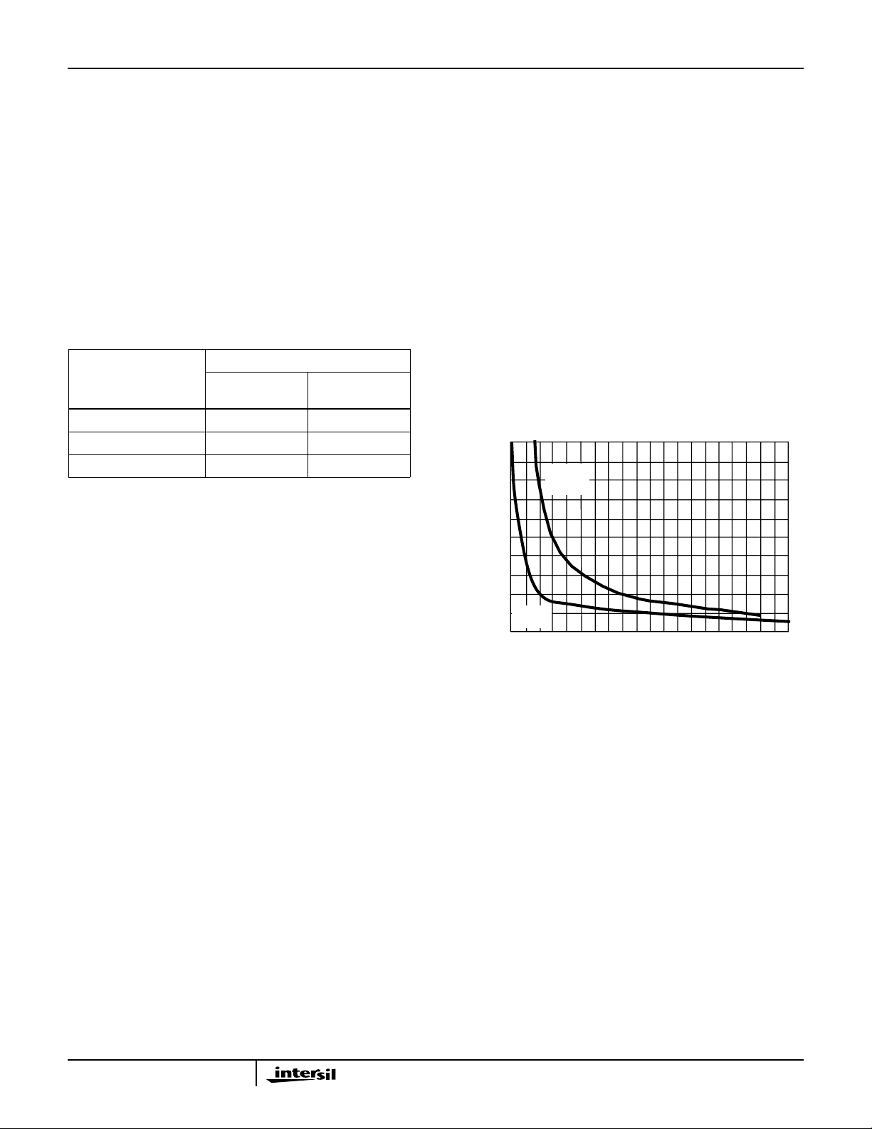
avoided by placing a resistor (R
) in series with the output
S
prior to the capacitance.
Figure 1 details starting points for the selection of this
resistor. The points on the curve indicate the R
and C
S
L
combinations for the optimum bandwidth, stability, and
settling time, but experimental fine tuning is recommended.
Picking a point above or to the right of the curve yields an
overdampedresponse, while points below or left of the curve
indicate areas of underdamped performance.
R
and CLform a low pass network at the output, thus
S
limiting system bandwidth well belowthe amplifier bandwidth
of 850MHz. By decreasing R
as CLincreases (as illustrated
S
in the curves), the maximum bandwidth is obtained without
sacrificing stability. Even so, bandwidth does decrease as
you move to the right along the curve. For example, at
A
= +1, RS = 50Ω, CL = 30pF, the overall bandwidth is
V
limited to 300MHz, and bandwidth drops to 100MHz at
A
= +1, RS = 5Ω, CL = 340pF.
V
50
45
40
35
30
25
(Ω)
S
20
R
15
10
5
0
0 40 80 120 160 200 240 280 320 360 400
FIGURE 1. RECOMMENDED SERIES RESISTOR vs LOAD
AV = +1
AV = +2
LOAD CAPACITANCE (pF)
CAPACITANCE
For unity gain applications, care must also be taken to
minimize the capacitance to ground seen by the amplifier’s
inverting input. At higher frequencies this capacitance will
tend to short the -INPUT to GND, resulting in a closed loop
gain which increases with frequency. This will cause
excessive high frequency peaking and potentially other
problems as well.
An example of a good high frequency layout is the
Evaluation Board shown in Figure 3.
Driving Capacitive Loads
Capacitive loads, such as an A/D input, or an improperly
terminated transmission line will degrade the amplifier’s
phase margin resulting in frequency response peaking and
possible oscillations. In most cases, the oscillation can be
5
Evaluation Board
The performance of the HFA1113 may be evaluated using
the HFA11XX Evaluation Board, slightly modified as follows:
1. Remove the 500Ω feedback resistor (R
connection open.
2. a. For A
resistor (R
b. For A
= +1 evaluation, remove the 500Ω gain setting
V
), and leave pin 2 floating.
1
=+2, replace the 500Ω gain setting resistor with
V
a 0Ω resistor to GND.
The modified schematic and layout of the board are shown
in Figures 2 and 3.
To order evaluation boards (part number HFA11XXEVAL),
please contact your local sales office.
NOTE: The SOIC version may be evaluated in the DIP board by
using a SOIC-to-DIP adapter such as Aries Electronics Part Number
08-350000-10.
), and leave the
2
Page 6

HFA1113
.
∞ (A
= +1)
V
OR 0Ω (A
IN
= +2)
V
V
R
1
1
50Ω
0.1µF0µF
2
3
4
-5V
8
7
6
5
GND
H
50Ω
GND
FIGURE 2. MODIFIED EVALUATION BOARD SCHEMATIC
TOP LAYOUT
V
H
1
+IN
OUT
V
L
V+
V-
GND
BOTTOM LAYOUT
OUT
V
L
between the positive and negative inputs. This buffer forces
-IN to track +IN, and sets up a slewing current of:
- V
(V
-IN
10µF0.1µF
+5V
This current is mirrored onto the high impedance node (Z) by
Q
X3-QX4
)/RF + V
OUT
-IN/RG
, where it is converted to a voltage and fed to the
output via another unity gain buffer. If no clamping is utilized,
the high impedance node may swing within the limits defined
by Q
and QN4. Note that when the output reaches its
P4
quiescent value, the current flowing through -IN is reduced to
only that small current (-I
) required to keep the output at
BIAS
the final voltage.
Tracing the path from V
clamp voltage on the high impedance node. V
by 2V
+IN
BE(QN6
and QP6) to set up the base voltage on QP5.
Q
P3
Q
P1
VV+
Q
N1
to Z illustrates the effect of the
H
V+
Q
P4
Q
N2
I
CLAMP
Q
P2
Z
+1
Q
N5
Q
Q
H
50K
(30K
FOR VL)
N6
P6
decreases
R
1
200Ω
V
H
FIGURE 3. EVALUATION BOARD LAYOUT
Limiting Operation
General
The HFA1113 features user programmable output clamps to
limit output voltage excursions. Clamping action is obtained
by applying voltages to the V
5) of the amplifier. V
sets the upper output limit, while V
H
sets the lower clamp level. If the amplifier tries to drive the
output above V
output voltage at V
, or below VL, the clamp circuitry limits the
H
or VL (± the clamp accuracy),
H
respectively. The low input bias currents of the clamp pins
allow them to be driven by simple resistive divider circuits, or
active elements such as amplifiers or DACs.
Clamp Circuitry
Figure 4 shows a simplified schematic of the HFA1113 input
stage, and the high clamp (V
feedback amplifiers, there is a unity gain buffer (Q
and VL terminals (pins 8 and
H
) circuitry. As with all current
H
- QX2)
X1
L
Q
Q
N3
V
V-
300Ω
-IN
R
(INTERNAL)
-IN
P5
Q
N4
G
RF= 300Ω
(INTERNAL)
V
OUT
FIGURE 4. HFA1113 SIMPLIFIED VH CLAMP CIRCUITRY
begins to conduct whenever the high impedance node
Q
P5
reaches a voltage equal to Q
’s base voltage + 2VBE(Q
P5
P5
and QN5). Thus, QP5 clamps node Z whenever Z reaches
V
. R1 provides a pull-up network to ensure functionality
H
with the clamp inputs floating. A similar description applies to
the symmetrical low clamp circuitry controlled by V
.
L
When the output is clamped, the negative input continues to
source a slewing current (I
output to the quiescent voltage defined by the input. Q
) in an attempt to force the
CLAMP
P5
must sink this current while clamping, because the -IN
current is always mirrored onto the high impedance node.
The clamping current is calculated as:
I
CLAMP
= (V
- V
-IN
OUT CLAMPED
)/300Ω + V
-IN/RG
.
As an example, a unity gain circuit with VIN = 2V, and VH=1V,
would have I
(R
= ∞ because -IN is floated for unity gain applications).
G
Note that I
CLAMP
CC
= (2V - 1V)/300Ω + 2V/∞ = 3.33mA
will increase by I
when the output is
CLAMP
clamp limited.
6
Page 7

HFA1113
Clamp Accuracy
The clamped output voltage will not be exactly equal to the
voltage applied to V
mismatches, necessitate a clamp accuracy parameter which
is found in the device specifications. Clamp accuracy is a
function of the clamping conditions. Referring again to
Figure 4, it can be seen that one component of clamp
accuracy is the VBE mismatch between the Q
and the Q
transistors. If the transistors always ran at the
X5
same current level there would be no V
contribution to the inaccuracy. The Q
biased at a constant current, but as described earlier, the
current through Q
as I
increases, causing the clamped output voltage to
CLAMP
increase as well. I
(A
x VIN - V
VCL
degrades as the overdrive increases. As an example, the
specified accuracy of ±100mV (A
overdrivedegrades to ±240mV for a 3X (200%) overdrive,as
shown in Figure 43.
Consideration must also be given to the fact that the clamp
voltages have an affect on amplifier linearity. The
“Nonlinearity Near Clamp Voltage” curve, Figure 48,
illustrates the impact of several clamp levels on linearity.
or VL. Offset errors, mostly due to V
H
mismatch, and no
BE
transistors are
X6
is equivalent to I
X5
is a function of the overdrive level
CLAMP
OUT CLAMPED
CLAMP
), so clamp accuracy
= -1, VH = 1V) for a 1.6X
V
BE
transistors,
X6
. VBE increases
restrictions indicated in the specifications. For example, the
HFA1113 could be limited to ECL output levels by setting
V
= -0.8V and VL= -1.8V. VHand VLmay be connected to
H
the same voltage (GND for instance) but the result won’t be
in a DC output voltage from an AC input signal. A
150mV - 200mV AC signal will still be present at the output.
Recovery from Overdrive
The output voltage remains at the clamp level as long as the
overdrive condition remains. When the input voltage drops
below the overdrive level (V
CLAMP/AVCL
return to linear operation. A time delay, known as the
Overdrive Recovery Time, is required for this resumption of
linear operation. The plots of “Unclamped Performance” and
“Clamped Performance” (Figures 41 and 42) highlight the
HFA1113’s subnanosecond recovery time. The difference
between the unclamped and clamped propagation delays is
the overdrive recovery time. The appropriate propagation
delays are 8.0ns for the unclamped pulse, and 8.8ns for the
clamped (2X overdrive) pulse yielding an overdrive recovery
time of 800ps. The measurement uses the 90% point of the
output transition to ensure that linear operation has
resumed. Note: The propagation delay illustrated is
dominated by the fixturing. The delta shown is accurate, but
the true HFA1113 propagation delay is 500ps.
) the amplifier will
Clamp Range
Unlike some competitor devices, both VH and VL have
usableranges that cross 0V. While V
than V
, both may be positive or negative, within the range
L
Typical Performance Curves V
200
AV = +2
150
100
50
0
-50
-100
OUTPUT VOLTAGE (mV)
-150
-200
TIME (5ns/DIV.)
FIGURE 5. SMALL SIGNAL PULSE RESPONSE FIGURE 6. LARGE SIGNAL PULSE RESPONSE
must be more positive
H
= ±5V, TA = 25oC, RL = 100Ω, Unless Otherwise Specified
SUPPLY
Overdrive recovery time is also a function of the overdrive
level. Figure 47 details the overdrive recovery time for
various clamp and overdrive levels.
2.0
AV = +2
1.5
1.0
0.5
0
-0.5
OUTPUT VOLTAGE (V)
-1.0
-1.5
-2.0
TIME (5ns/DIV.)
7
Page 8

HFA1113
Typical Performance Curves V
200
AV = +1
150
100
50
0
-50
-100
OUTPUT VOLTAGE (mV)
-150
-200
TIME (5ns/DIV.)
FIGURE 7. SMALL SIGNAL PULSE RESPONSE FIGURE 8. LARGE SIGNAL PULSE RESPONSE
200
AV = -1
150
100
= ±5V, TA = 25oC, RL = 100Ω, Unless Otherwise Specified (Continued)
SUPPLY
2.0
= +1
A
V
1.5
1.0
0.5
0
-0.5
OUTPUT VOLTAGE (V)
-1.0
-1.5
-2.0
2.0
1.5
1.0
AV = -1
TIME (5ns/DIV.)
50
0
-50
-100
OUTPUT VOLTAGE (mV)
-150
-200
TIME (5ns/DIV.)
0.5
-0.5
OUTPUT VOLTAGE (V)
-1.0
-1.5
-2.0
0
TIME (5ns/DIV.)
FIGURE 9. SMALL SIGNAL PULSE RESPONSE FIGURE 10. LARGE SIGNAL PULSE RESPONSE
6
V
= 200mV
OUT
3
GAIN
0
-3
-6
-9
NORMALIZED GAIN (dB)
PHASE
0.3 1 10 100 1000
P-P
FREQUENCY (MHz)
AV = +1
A
= +2
V
= -1
A
V
AV = +1
AV = -1
A
= +2
V
0
-90
-180
-270
-360
NORMALIZED PHASE (DEGREES)
AV = +2, V
9
6
3
GAIN (dB)
0
0.3 1 10 100 1000
= 200mV
OUT
GAIN
PHASE
FREQUENCY (MHz)
P-P
= 50Ω
R
L
= 100Ω
R
L
RL = 1kΩ
RL = 100Ω
R
= 50Ω
L
R
= 1kΩ
L
0
-90
-180
-270
PHASE (DEGREES)
-360
FIGURE 11. FREQUENCY RESPONSE FIGURE 12. FREQUENCY RESPONSE FOR VARIOUS LOAD
RESISTORS
8
Page 9

HFA1113
Typical Performance Curves V
6
AV = +1, V
3
GAIN
OUT
= 200mV
P-P
= ±5V, TA = 25oC, RL = 100Ω, Unless Otherwise Specified (Continued)
SUPPLY
0
= 1kΩ
R
-3
GAIN (dB)
-6
-9
L
RL = 100Ω
= 50Ω
R
L
PHASE
R
= 100Ω
L
= 50Ω
R
L
R
= 1kΩ
L
0.3 1 10 100 1000
FREQUENCY (MHz)
FIGURE 13. FREQUENCY RESPONSE FOR VARIOUS LOAD
RESISTORS
12
AV = +2
9
6
3
GAIN (dB)
0
GAIN
PHASE
4.0V
2.5V
1V
4.0V
2.5V
P-P
P-P
P-P
P-P
P-P
1V
P-P
0
-90
-180
-270
-360
0
-90
-180
-270
-360
PHASE (DEGREES)
PHASE (DEGREES)
6
AV = -1, V
3
0
-3
GAIN (dB)
-6
GAIN
OUT
= 200mV
P-P
RL = 1kΩ
RL = 100Ω
R
L
= 50Ω
-9
PHASE
RL = 100Ω
180
90
= 50Ω
R
L
RL = 1kΩ
0.3 1 10 100 1000
0
-90
-180
FREQUENCY (MHz)
FIGURE 14. FREQUENCY RESPONSE FOR VARIOUS LOAD
RESISTORS
6
AV = +1
3
0
-3
GAIN (dB)
-6
GAIN
PHASE
V
V
V
OUT
OUT
OUT
V
OUT
V
OUT
V
OUT
= 4V
= 2.5V
= 1V
= 4V
= 2.5V
= 1V
P-P
P-P
P-P
P-P
P-P
P-P
0
-90
-180
-270
-360
PHASE (DEGREES)
PHASE (DEGREES)
0.3 1 10 100 1000
FREQUENCY (MHz)
FIGURE15. FREQUENCYRESPONSEFOR VARIOUSOUTPUT
VOLTAGES
6
AV = -1
3
0
-3
GAIN (dB)
-6
GAIN
PHASE
V
V
V
OUT
OUT
OUT
= 2.5V
= 4V
= 1V
P-P
P-P
P-P
180
90
V
= 4V
OUT
V
V
OUT
OUT
= 2.5V
= 1V
P-P
P-P
P-P
0
-90
-180
0.3 1 10 100 1000
FREQUENCY (MHz)
FIGURE17. FREQUENCYRESPONSEFOR VARIOUSOUTPUT
VOLTAGES
FIGURE16. FREQUENCYRESPONSEFOR VARIOUSOUTPUT
NORMALIZED GAIN (dB)
PHASE (DEGREES)
0.3 1 10 100 1000
FREQUENCY (MHz)
VOLTAGES
15
V
= 5V
OUT
12
P-P
9
6
3
0
-3
-6
= -1
A
V
= +2
A
V
AV = +1
-9
-12
-15
0.3 1 10 100 1000
FREQUENCY (MHz)
FIGURE 18. FULL POWER BANDWIDTH
9
Page 10

HFA1113
Typical Performance Curves V
900
850
800
750
700
650
BANDWIDTH (MHz)
600
550
500
-50 -25 0 25 50 75 100 125
AV = +1
AV = -1
AV = +2
TEMPERATURE (
o
C)
= ±5V, TA = 25oC, RL = 100Ω, Unless Otherwise Specified (Continued)
SUPPLY
0.35
0.30
0.25
0.20
0.15
0.10
0.05
0
NORMALIZED GAIN (dB)
-0.05
-0.10
-0.15
1 10 100
FREQUENCY (MHz)
FIGURE 19. -3dB BANDWIDTH vs TEMPERATURE FIGURE 20. GAIN FLATNESS
4
3
2
1
0
-1
-2
-3
DEVIATION (DEGREES)
-4
-5
-6
0 15 30 45 60 75 90 105 120 135
FREQUENCY (MHz)
AV = +1
AV = -1
AV = +2
150
AV = +2, V
0.6
0.4
0.2
0.1
0
-0.1
-0.2
-0.4
SETTLING ERROR (%)
-0.6
-2 3 8 13 18 23 28 33 38 43 48
OUT
AV = +1
= 2V
TIME (ns)
AV = -1
AV = +2
FIGURE 21. DEVIATION FROM LINEAR PHASE FIGURE 22. SETTLING RESPONSE
-24
-30
-36
-42
-48
-54
-60
GAIN (dB)
-66
AV = +2
-72
-78
-84
0
AV = +1
AV = -1
20 40 60 80 100 120 140 160 180 200
FREQUENCY (MHz)
AV = +2
AV = -1
PHASE
AV = -1
-24
-30
-36
-42
-48
GAIN (dB)
-54
-60
100 190 280 370 460 550 640 730 820 910 1000
AV = +2
GAIN
AV = -1
FREQUENCY (MHz)
AV = -1
AV = +1
AV = +2
235
180
90
45
0
FIGURE 23. LOW FREQUENCY REVERSE ISOLATION (S12) FIGURE 24. HIGH FREQUENCY REVERSE ISOLATION (S12)
10
PHASE (DEGREES)
Page 11

HFA1113
Typical Performance Curves V
20
18
16
14
12
10
8
6
4
2
0
OUTPUT POWER AT 1dB COMPRESSION (dBm)
100 200 300 400 500
AV = +2
AV = +1
AV = -1
FREQUENCY (MHz)
= ±5V, TA = 25oC, RL = 100Ω, Unless Otherwise Specified (Continued)
SUPPLY
30
20
10
INTERCEPT POINT (dBm)
0
100 200 300 400
2 - TONE
AV = +1
FREQUENCY (MHz)
AV = -1
AV = +2
FIGURE 25. 1dB GAIN COMPRESSION vs FREQUENCY FIGURE 26. THIRD ORDER INTERMODULATIONINTERCEPT
vs FREQUENCY
-20
AV = +2
-30
-40
-50
-60
-70
DISTORTION (dBc)
-80
-90
-100
-6 -3 0 3 6 9 12 15
100MHz
OUTPUT POWER (dBm)
50MHz
30MHz
-20
AV = +2
-30
-40
-50
-60
-70
DISTORTION (dBc)
-80
-90
-100
-6 -3 0 3 6 9 12 15 18
100MHz
OUTPUT POWER (dBm)
50MHz
30MHz
FIGURE 27. SECOND HARMONIC DISTORTION vs P
-20
AV = +1
-30
-40
-50
-60
-70
DISTORTION (dBc)
-80
-90
-100
-6 -3 0 3 6 9 12 15
100MHz
50MHz
OUTPUT POWER (dBm)
30MHz
FIGURE 29. SECOND HARMONIC DISTORTION vs P
11
OUT
OUT
FIGURE 28. THIRD HARMONIC DISTORTION vs P
-20
AV = +1
-30
-40
-50
-60
-70
DISTORTION (dBc)
-80
-90
-100
-6 -3 0 3 6 9 12 15
100MHz
50MHz
OUTPUT POWER (dBm)
30MHz
FIGURE 30. THIRD HARMONIC DISTORTION vs P
OUT
OUT
Page 12

HFA1113
Typical Performance Curves V
-20
-30
-40
-50
-60
-70
DISTORTION (dBc)
-80
-90
-100
FIGURE 31. SECOND HARMONIC DISTORTION vs P
0.04
0.02
AV = -1
100MHz
-6 -3 0 3 6 9 12 15
50MHz
30MHz
OUTPUT POWER (dBm)
= ±5V, TA = 25oC, RL = 100Ω, Unless Otherwise Specified (Continued)
SUPPLY
OUT
-20
-30
-40
-50
-60
-70
DISTORTION (dBc)
-80
-90
-100
FIGURE 32. THIRD HARMONIC DISTORTION vs P
60
50
40
AV = -1
100MHz
-6 -3 0 3 6 9 12 15
V
= 0.5V
OUT
50MHz
OUTPUT POWER (dBm)
AV = +1
30MHz
OUT
PERCENT ERROR (%)
-0.02
-0.04
0
-3.0
-2.0 -1.0 0 1.0 2.0 3.0
INPUT VOLTAGE (V)
30
20
OVERSHOOT (%)
10
AV = +2
0
100 300 500 700 900 1100 1300
AV = -1
INPUT RISE TIME (ps)
FIGURE 33. INTEGRAL LINEARITY ERROR FIGURE 34. OVERSHOOT vs INPUT RISE TIME
60
V
= 1V
OUT
50
40
30
20
OVERSHOOT (%)
AV = -1
10
0
100 300 500 700 900 1100 1300
AV = +2
INPUT RISE TIME (ps)
AV = +1
60
V
= 2V
OUT
50
40
AV = +1
30
AV = -1
20
OVERSHOOT (%)
AV = +2
10
0
100 300 500 700 900 1100 1300
INPUT RISE TIME (ps)
FIGURE 35. OVERSHOOT vs INPUT RISE TIME FIGURE 36. OVERSHOOT vs INPUT RISE TIME
12
Page 13

HFA1113
Typical Performance Curves V
22
21
20
19
18
17
16
15
14
13
12
11
10
9
SUPPLY CURRENT (mA)
8
7
6
5
59
678 10
TOTAL SUPPLY VOLTAGE (V+ - V-, V)
= ±5V, TA = 25oC, RL = 100Ω, Unless Otherwise Specified (Continued)
SUPPLY
FIGURE 37. SUPPLY CURRENT vs SUPPLY VOLTAGE
3.6
AV = -1
3.5
+V
3.4
3.3
3.2
3.1
3.0
2.9
OUTPUT VOLTAGE (V)
2.8
2.7
2.6
|-V
| (RL= 100Ω)
OUT
|-V
| (RL= 50Ω)
OUT
-50 -25 0 25 50 75 100 125
TEMPERATURE (
(RL= 50Ω)
OUT
+V
o
(RL= 100Ω)
OUT
C)
25
24
23
22
21
20
19
18
SUPPLY CURRENT (mA)
17
16
15
-50 -25 0 25 50 75 100 125
TEMPERATURE (
o
C)
FIGURE 38. SUPPLY CURRENT vs TEMPERATURE
50
40
30
20
E
NOISE VOLTAGE (nV/√Hz)
10
0
0.1 1 10 100
FREQUENCY (kHz)
NI
I
NI
130
110
90
70
50
30
NOISE CURRENT (pA/√Hz)
FIGURE 39. OUTPUT VOLTAGE vs TEMPERATURE FIGURE 40. INPUT NOISE CHARACTERISTICS
AV = +2
IN
0V TO
0.5V
OUT
0V TO
1V
TIME (20ns/DIV.)
0V TO
1V
OUT
0V TO
1V
IN
AV = +2
TIME (20ns/DIV.)
FIGURE 41. UNCLAMPED PERFORMANCE FIGURE 42. CLAMPED PERFORMANCE
13
Page 14

HFA1113
Typical Performance Curves V
350
AV = ±1
300
250
= 1V
V
200
150
100
CLAMP ACCURACY (mV)
50
0
0 100 200 300 400 500
OVERDRIVE (% OF V
H
= 2V
V
H
VH = 100mV
)
H
= ±5V, TA = 25oC, RL = 100Ω, Unless Otherwise Specified (Continued)
SUPPLY
250
AV = ±1
VH = 500mV
200
150
100
CLAMP ACCURACY (mV)
50
0
0
100 200 300 400 500
OVERDRIVE (% OF V
)
L
FIGURE 43. VH CLAMP ACCURACY vs OVERDRIVE FIGURE 44. VL CLAMP ACCURACY vs OVERDRIVE
400
300
200
A
= ±2
V
VH = 500mV
= 1V
V
H
V
= 2V
H
250
200
150
100
AV = +2
VL = -1V
= -2V
V
L
VL = -500mV
= -1V
V
L
= -2V
V
L
VL = -100mV
VL = -500mV
100
CLAMP ACCURACY (mV)
0
0 100 200 300 400 500
OVERDRIVE (% OF VH)
VH = 100mV
CLAMP ACCURACY (mV)
50
0
0 100 200 300 400 500
OVERDRIVE (% OF VL)
FIGURE 45. VH CLAMP ACCURACY vs OVERDRIVE FIGURE 46. VL CLAMP ACCURACY vs OVERDRIVE
3500
3000
2500
2000
1500
1000
500
OVERDRIVE RECOVERY TIME (ps)
0
100 200 300 400 500
OVERDRIVE LEVEL (% OF CLAMP LEVEL)
V
= 2V
H
VH = 1V
VH = 0.1V
V
= 0.5V
H
20
15
VL = -3V
10
) (mV)
5
IN
x V
0
V
- (A
-5
OUT
V
-10
-15
-20
-3 -2 -1 0 1 2 3
VL = -2V
VL = -1V
VH = 1V
x VIN (V)
A
V
VH = 2V
VL = -100mV
AV = -1
VH = 3V
FIGURE 47. OVERDRIVE RECOVERY vs OVERDRIVE FIGURE 48. NON-LINEARITY NEAR CLAMP VOLTAGE
14
Page 15

HFA1113
Typical Performance Curves V
140
AV = -1, VIN = ±1.6V
= 1V, VL = -1V
V
130
H
120
110
100
90
80
CLAMP ACCURACY (mV)
70
60
-75
-25
-50 0 50 100 150
TEMPERATURE (oC)
V
H
V
L
25
= ±5V, TA = 25oC, RL = 100Ω, Unless Otherwise Specified (Continued)
SUPPLY
130
120
110
100
90
80
70
60
50
CLAMP BIAS CURRENT (µA)
40
30
12575
20
-75
-25
-50 0 50 100 150
V
L
V
H
25
TEMPERATURE (oC)
VH = 1V, VL = -1V
FIGURE 49. CLAMP ACCURACY vs TEMPERATURE FIGURE 50. CLAMP BIAS CURRENT vs TEMPERATURE
6
3
0
-3
GAIN (dB)
-6
-9
-12
VH = 600mV
VH = 1.2V
P-P
P-P
VH = 300mV
P-P
6
3
0
-3
GAIN (dB)
-6
-9
-12
VL = 600mV
VL = 1.2V
VL = 300mV
P-P
P-P
12575
P-P
1 10 100 1000
FREQUENCY (MHz)
FIGURE 51. VH CLAMP INPUT BANDWIDTH
15
1 10 100 1000
FREQUENCY (MHz)
FIGURE 52. VL CLAMP INPUT BANDWIDTH
Page 16

Die Characteristics
HFA1113
DIE DIMENSIONS:
63 mils x 44 mils x 19 mils
1600µm x 1130µm x 483µm
METALLIZATION:
Type: Metal 1: AICu(2%)/TiW
Thickness: Metal 1: 8k
Å ±0.4kÅ
Type: Metal 2: AICu(2%)
Thickness: Metal 2: 16k
Å ±0.8kÅ
Metallization Mask Layout
PASSIVATION:
Type: Nitride
Thickness: 4k
Å ±0.5kÅ
TRANSISTOR COUNT:
52
SUBSTRATE POTENTIAL (POWERED UP):
Floating (Recommend Connection to V-)
HFA1113
NC
+IN
V-
NC
V
L
OUT
-IN
V
V+
H
16
Page 17

Small Outline Plastic Packages (SOIC)
HFA1113
N
INDEX
AREA
123
-A-
E
-B-
SEATING PLANE
D
A
-C-
0.25(0.010) BM M
H
L
h x 45
o
α
e
B
0.25(0.010) C AM BS
M
NOTES:
1. Symbols are defined in the “MO Series Symbol List” in Section 2.2 of
Publication Number 95.
2. Dimensioning and tolerancing per ANSI Y14.5M-1982.
3. Dimension “D” does not include mold flash, protrusions or gate burrs.
Mold flash, protrusion and gate burrs shall not exceed 0.15mm (0.006
inch) per side.
4. Dimension “E” does not include interlead flash or protrusions. Interlead flash and protrusions shall not exceed 0.25mm (0.010 inch) per
side.
5. The chamfer on the body is optional. If it is not present, a visual index
feature must be located within the crosshatched area.
6. “L” is the length of terminal for soldering to a substrate.
7. “N” is the number of terminal positions.
8. Terminal numbers are shown for reference only.
9. The lead width “B”, as measured 0.36mm (0.014 inch) or greater
above the seating plane, shall not exceed a maximum value of
0.61mm (0.024 inch).
10. Controlling dimension: MILLIMETER. Converted inch dimensions
are not necessarily exact.
A1
C
0.10(0.004)
M8.15 (JEDEC MS-012-AA ISSUE C)
8 LEAD NARROW BODY SMALL OUTLINE PLASTIC
PACKAGE
INCHES MILLIMETERS
SYMBOL
A 0.0532 0.0688 1.35 1.75 -
A1 0.0040 0.0098 0.10 0.25 -
B 0.013 0.020 0.33 0.51 9
C 0.0075 0.0098 0.19 0.25 D 0.1890 0.1968 4.80 5.00 3
E 0.1497 0.1574 3.80 4.00 4
e 0.050 BSC 1.27 BSC H 0.2284 0.2440 5.80 6.20 h 0.0099 0.0196 0.25 0.50 5
L 0.016 0.050 0.40 1.27 6
N8 87
o
α
0
o
8
o
0
o
8
Rev. 0 12/93
NOTESMIN MAX MIN MAX
-
All Intersil semiconductor products are manufactured, assembled and tested under ISO9000 quality systems certification.
Intersil semiconductor products are sold by description only.Intersil Corporation reserves the right to make changes in circuit design and/or specifications at any time without notice. Accordingly, the reader is cautioned to verify that data sheets are current before placing orders. Information furnished by Intersil is believed to be accurate and
reliable. However, no responsibility is assumed by Intersil or its subsidiaries for its use; nor for any infringements of patents or other rights of third parties which may result
from its use. No license is granted by implication or otherwise under any patent or patent rights of Intersil or its subsidiaries.
For information regarding Intersil Corporation and its products, see web site www.intersil.com
Sales Office Headquarters
NORTH AMERICA
Intersil Corporation
P. O. Box 883, Mail Stop 53-204
Melbourne, FL 32902
TEL: (321) 724-7000
FAX: (321) 724-7240
17
EUROPE
Intersil SA
Mercure Center
100, Rue de la Fusee
1130 Brussels, Belgium
TEL: (32) 2.724.2111
FAX: (32) 2.724.22.05
ASIA
Intersil (Taiwan) Ltd.
7F-6, No. 101 Fu Hsing North Road
Taipei, Taiwan
Republic of China
TEL: (886) 2 2716 9310
FAX: (886) 2 2715 3029
 Loading...