Intersil Corporation HFA1112-883 Datasheet
June 1994
HFA1112/883
Ultra High Speed
Programmable Gain Buffer Amplifier
Features
• This Circuit is Processed in Accordance to MIL-STD883 and is Fully Conformant Under the Provisions of
Paragraph 1.2.1.
• User Programmable For Closed-Loop Gains of +1, -1
or +2 Without Use of External Resistors
• Low Differential Gain and Phase . . . . 0.02%/0.04 Deg.
• Low Distortion (HD3, 30MHz) . . . . . . . . . . -73dBc (Typ)
• Wide -3dB Bandwidth . . . . . . . . . . . . . . . 850MHz (Typ)
• Very High Slew Rate . . . . . . . . . . . . . . . 2400V/µs (Typ)
• Fast Settling (0.1%) . . . . . . . . . . . . . . . . . . . . 13ns (Typ)
• Excellent Gain Flatness (to 100MHz) . . . . 0.07dB (Typ)
• Excellent Gain Accuracy. . . . . . . . . . . . . .0.99V/V (Typ)
• High Output Current . . . . . . . . . . . . . . . . . . 60mA (Typ)
• Fast Overdrive Recovery. . . . . . . . . . . . . . . <10ns (Typ)
Applications
• Video Switching and Routing
• Pulse and Video Amplifiers
• Wideband Amplifiers
• RF/IF Signal Processing
• Flash A/D Driver
• Medical Imaging Systems
Description
The HFA1112/883 is a closed loop buffer that achieves a
high degree of gain accuracy, wide bandwidth, and low distortion. Manufactured on the Intersil proprietary complementary bipolar UHF-1 process, the HFA1112/883 also offers
very fast slew rates, and high output current.
A unique feature of the pinout allows the user to select a voltage gain of +1, -1, or +2, without the use of any external
components. The result is a more flexible product, fewer part
types in inventory, and more efficient use of board space.
Component and composite video systems will also benefit
from this buffer’s performance, as indicated by the excellent
gain flatness, and 0.02%/0.04 Deg. Differential Gain/Phase
specifications (R
Compatibility with existing op amp pinouts provides flexibility
to upgrade low gain amplifiers, while decreasing component
count. Unlike most buffers, the standard pinout provides an
upgrade path should a higher closed loop gain be needed at
a future date.
This amplifier is available with programmable output clamps
as the HFA1113/883. For applications requiring a standard
buffer pinout, please refer to the HFA1110/883 datasheet.
= 150Ω).
L
Ordering Information
TEMPERATURE
PART NUMBER
HFA1112MJ/883 -55oC to +125oC 8 Lead Ceramic DIP
RANGE PACKAGE
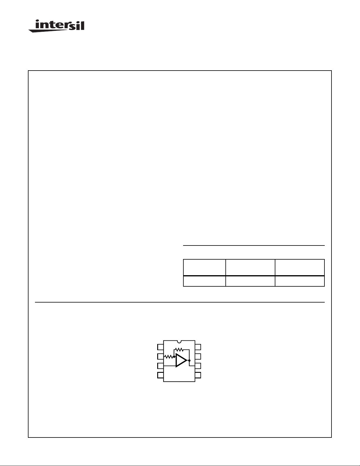
Pinout
HFA1112/883
(CERDIP)
TOP VIEW
NC
-IN
+IN
V-
CAUTION: These devices are sensitive to electrostatic discharge; follow proper IC Handling Procedures.
http://www.intersil.com or 407-727-9207
| Copyright © Intersil Corporation 1999
300
1
300
2
3
4
3-184
8
NC
-
7
+
V+
6
OUT
5
NC
Spec Number 511084-883
File Number 3610.1
Specifications HFA1112/883
Absolute Maximum Ratings Thermal Information
Voltage Between V+ and V- . . . . . . . . . . . . . . . . . . . . . . . . . . . . 12V
Differential Input Voltage . . . . . . . . . . . . . . . . . . . . . . . . . . . . . . . 5V
Voltage at Either Input Terminal . . . . . . . . . . . . . . . . . . . . . . V+ to V-
Output Current (50% Duty Cycle) . . . . . . . . . . . . . . . . . . . . . . . .±55mA
Junction Temperature. . . . . . . . . . . . . . . . . . . . . . . . . . . . . . +175oC
ESD Rating. . . . . . . . . . . . . . . . . . . . . . . . . . . . . . . . . . . . . . <2000V
Storage Temperature Range . . . . . . . . . . . . . . -65oC ≤ TA≤ +150oC
Lead Temperature (Soldering 10s). . . . . . . . . . . . . . . . . . . . +300oC
CAUTION: Stresses above those listed in “Absolute Maximum Ratings” may cause permanent damage to the device. This is a stress only rating and operation
of the device at these or any other conditions above those indicated in the operational sections of this specification is not implied.
Operating Conditions
Operating Supply Voltage (±VS) . . . . . . . . . . . . . . . . . . . . . . . . . . . ±5V
Operating Temperature Range. . . . . . . . . . . . .-55oC ≤ TA≤ +125oC
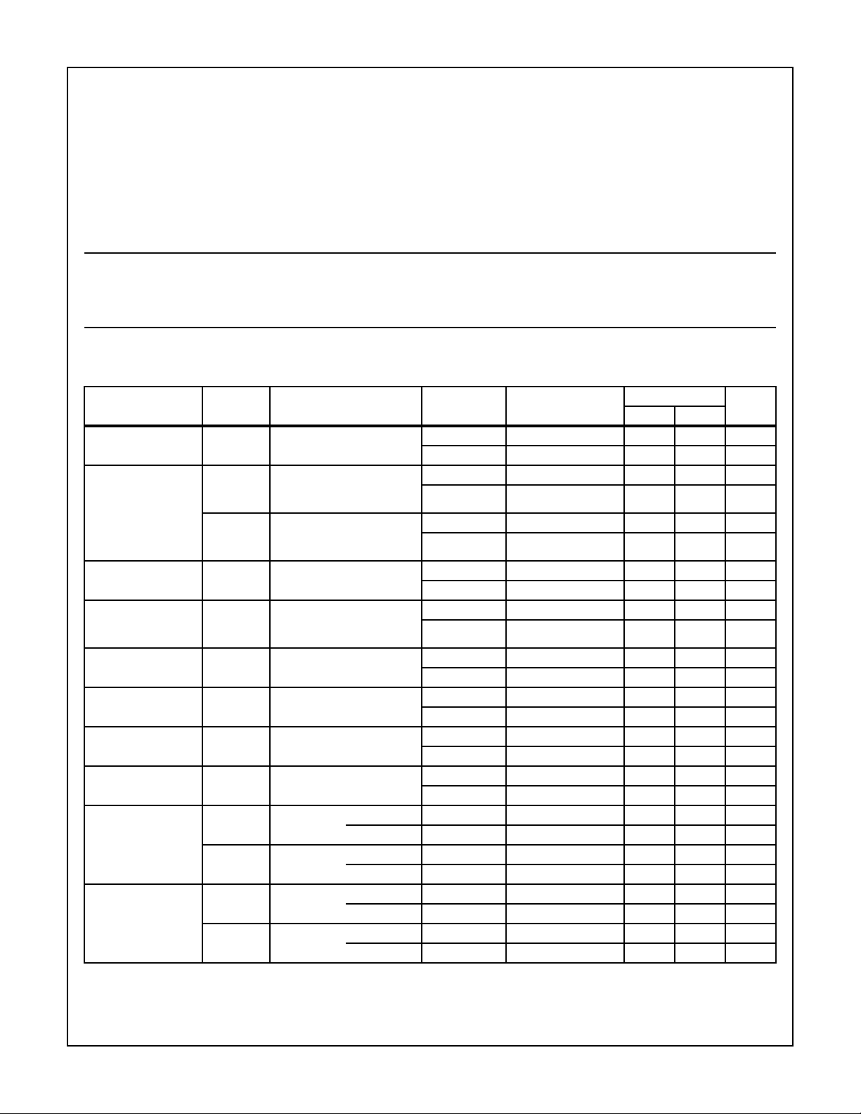
TABLE 1. DC ELECTRICAL PERFORMANCE CHARACTERISTICS
Device Tested at V
D.C. PARAMETERS SYMBOL CONDITIONS
Output Offset Voltage V
Power Supply
Rejection Ratio
Non-Inverting Input
(+IN) Current
+IN Common
Mode Rejection
+IN Resistance +R
Gain
(V
= 2V
OUT
P-P
)
Gain
(V
=2V
OUT
P-P
)
Gain
(V
= 4V
OUT
P-P
)
Output Voltage
Swing
Output Voltage
Swing
SUPPLY
= ±5V, R
SOURCE
OS
PSRRP ∆V
PSRRN ∆V
I
BSP
CMS
IBP
IN
A
VP1
A
VM1
A
VP2
V
OP100
V
ON100
V
OP50
V
ON50
= 0Ω, RL = 100Ω, V
VCM = 0V 1 +25oC -25 25 mV
= ±1.25V
SUP
V+ = 6.25V, V- = -5V
V+ = 3.75V, V- = -5V
= ±1.25V
SUP
V+ = 5V, V- = -6.25V
V+ = 5V, V- = -3.75V
VCM = 0V 1 +25oC -40 40 µA
∆VCM = ±2V
V+ = 3V, V- = -7V
V+ = 7V, V- = -3V
Note 1 1 +25oC25-kΩ
AV = +1
VIN = -1V to +1V
AV = -1
VIN = -1V to +1V
AV = +2
VIN = -1V to +1V
AV = -1
RL = 100Ω
AV = -1
RL = 100Ω
AV = -1
RL = 50Ω
AV = -1
RL = 50Ω
VIN = -3.2V 1 +25oC3-V
VIN = -2.7V 2, 3 +125oC, -55oC 2.5 - V
VIN = +3.2V 1 +25oC - -3 V
VIN = +2.7V 2, 3 +125oC, -55oC - -2.5 V
VIN = -2.7V 1, 2 +25oC, +125oC 2.5 - V
VIN = -2.25V 3 -55oC 1.5 - V
VIN = +2.7V 1, 2 +25oC, +125oC - -2.5 V
VIN = +2.25V 3 -55oC - -1.5 V
Thermal Resistance θ
CerDIP Package . . . . . . . . . . . . . . . . . 115oC/W 30oC/W
Maximum Package Power Dissipation at +75oC
CerDIP Package . . . . . . . . . . . . . . . . . . . . . . . . . . . . . . . . .0.87W
Package Power Dissipation Derating Factor above +75oC
CerDIP Package . . . . . . . . . . . . . . . . . . . . . . . . . . . . . .8.7mW/oC
RL ≥ 50Ω
= 0V, Unless Otherwise Specified.
OUT
GROUP A
SUBGROUPS TEMPERATURE
2, 3 +125oC, -55oC -40 40 mV
1 +25oC39-dB
2, 3 +125oC, -55oC35-dB
1 +25oC39-dB
2, 3 +125oC, -55oC35-dB
2, 3 +125oC, -55oC -65 65 µA
1 +25oC-40µA/V
2, 3 +125oC, -55oC-50µA/V
2, 3 +125oC, -55oC20-kΩ
1 +25oC 0.980 1.020 V/V
2, 3 +125oC, -55oC 0.975 1.025 V/V
1 +25oC 0.980 1.020 V/V
2, 3 +125oC, -55oC 0.975 1.025 V/V
1 +25oC 1.960 2.040 V/V
2, 3 +125oC, -55oC 1.950 2.050 V/V
JA
LIMITS
θ
JC
UNITSMIN MAX
3-185
Spec Number 511084-883
Specifications HFA1112/883
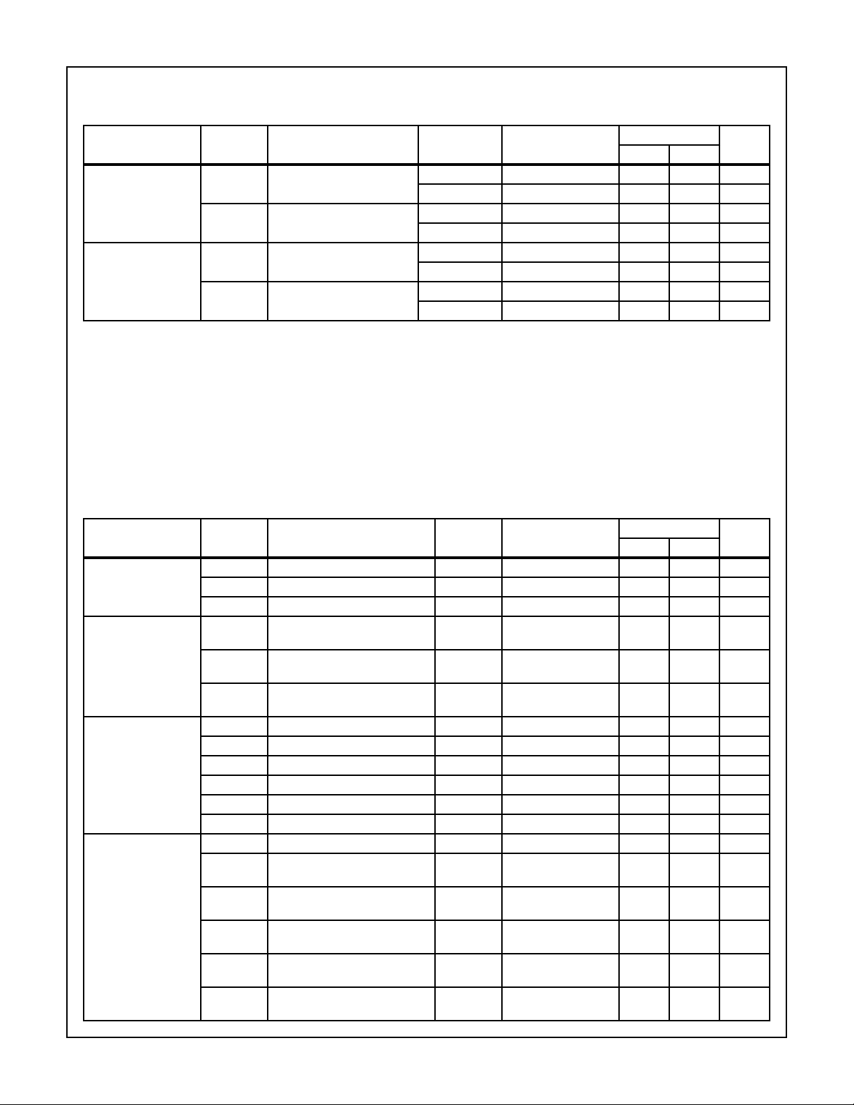
TABLE 1. DC ELECTRICAL PERFORMANCE CHARACTERISTICS (Continued)
Device Tested at V
D.C. PARAMETERS SYMBOL CONDITIONS
Output Current +I
Quiescent Power
Supply Current
NOTES:
1. Guaranteed from +IN Common Mode Rejection Test, by: +RIN = 1/CMS
2. Guaranteed from V
Table 2 Intentionally Left Blank.
SUPPLY
= ±5V, R
OUT
-I
OUT
I
CC
I
EE
Test with RL = 50Ω, by: I
OUT
= 0Ω, RL = 100Ω, V
SOURCE
Note 2 1, 2 +25oC, +125oC50 -mA
Note 2 1, 2 +25oC, +125oC - -50 mA
RL = 100Ω 1 +25oC1426mA
RL = 100Ω 1 +25oC -26 -14 mA
TABLE 2. AC ELECTRICAL PERFORMANCE CHARACTERISTICS
OUT
= V
= 0V, Unless Otherwise Specified.
OUT
SUBGROUPS TEMPERATURE
/50Ω.
OUT
GROUP A
LIMITS
UNITSMIN MAX
3 -55oC30-mA
3 -55oC - -30 mA
2, 3 +125oC, -55oC - 33 mA
2, 3 +125oC, -55oC -33 - mA
.
IBP
TABLE 3. ELECTRICAL PERFORMANCE CHARACTERISTICS
Device Characterized at V
= ±5V, RL = 100Ω, Unless Otherwise Specified.
SUPPLY
PARAMETERS SYMBOL CONDITIONS NOTES TEMPERATURE
-3dB Bandwidth BW(-1) AV = -1, V
BW(+1) AV = +1, V
BW(+2) AV = +2, V
Gain Flatness GF30 AV = +2, f ≤ 30MHz
V
= 200mV
OUT
GF50 AV = +2, f ≤ 50MHz
V
= 200mV
OUT
GF100 AV = +2, f ≤ 100MHz
V
= 200mV
OUT
Slew Rate +SR(-1) AV = -1, V
-SR(-1) AV = -1, V
+SR(+1) AV = +1, V
-SR(+1) AV = +1, V
+SR(+2) AV = +2, V
-SR(+2) AV = +2, V
Rise and Fall Time TR(-1) AV = -1, V
TF(-1) AV = -1, V
OUT
OUT
OUT
OUT
OUT
OUT
OUT
OUT
OUT
OUT
OUT
= 200mV
= 200mV
= 200mV
P-P
P-P
P-P
= 5V
P-P
= 5V
P-P
= 5V
P-P
= 5V
P-P
= 5V
P-P
= 5V
P-P
= 0.5V
P-P
= 0.5V
P-P
P-P
P-P
P-P
1 +25oC 450 - MHz
1 +25oC 500 - MHz
1 +25oC 350 - MHz
1 +25oC-±0.04 dB
1 +25oC-±0.08 dB
1 +25oC-±0.22 dB
1, 2 +25oC 1500 - V/µs
1, 2 +25oC 1800 - V/µs
1, 2 +25oC 900 - V/µs
1, 2 +25oC 800 - V/µs
1, 2 +25oC 1200 - V/µs
1, 2 +25oC 1100 - V/µs
1, 2 +25oC - 750 ps
1, 2 +25oC - 800 ps
LIMITS
UNITSMIN MAX
TR(+1) AV = +1, V
TF(+1) AV = +1, V
TR(+2) AV = +2, V
TF(+2) AV = +2, V
OUT
OUT
OUT
OUT
= 0.5V
= 0.5V
= 0.5V
= 0.5V
P-P
P-P
P-P
P-P
1, 2 +25oC - 750 ps
1, 2 +25oC - 750 ps
1, 2 +25oC - 1000 ps
1, 2 +25oC - 1000 ps
Spec Number 511084-883
3-186
Specifications HFA1112/883
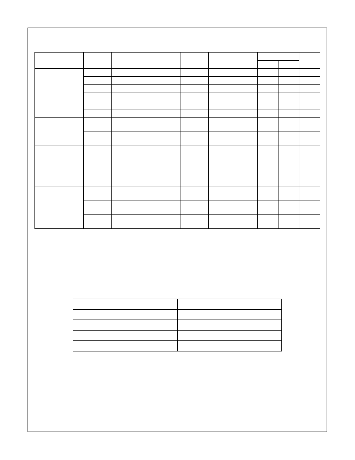
TABLE 3. ELECTRICAL PERFORMANCE CHARACTERISTICS (Continued)
Device Characterized at V
PARAMETERS SYMBOL CONDITIONS NOTES TEMPERATURE
Overshoot +OS(-1) AV = -1, V
Settling Time TS(0.1) AV = +2, to 0.1%
2nd Harmonic
Distortion
3rd Harmonic
Distortion
NOTES:
1. Parameters listed in Table 3 are controlled via design or process parameters and are not directly tested at final production. These parameters are lab characterized upon initial design release, or upon design changes. These parameters are guaranteed by characterization based upon data from multiple production runs which reflect lot-to-lot and within lot variation.
2. Measured between 10% and 90% points.
3. For 200ps input transition times. Overshoot decreases as input transition times increase, especially for AV = +1. Please refer to
Performance curves.
= ±5V, RL = 100Ω, Unless Otherwise Specified.
SUPPLY
= 0.5V
-OS(-1) AV = -1, V
+OS(+1) AV = +1, V
-OS(+1) AV = +1, V
+OS(+2) AV = +2, V
-OS(+2) AV = +2, V
V
= 2V to 0V
OUT
OUT
OUT
OUT
OUT
OUT
OUT
= 0.5V
= 0.5V
= 0.5V
= 0.5V
= 0.5V
P-P
P-P
P-P
P-P
P-P
P-P
TS(0.05) AV = +2, to 0.05%
V
= 2V to 0V
OUT
HD2(30) AV = +2, f = 30MHz
V
= 2V
OUT
P-P
HD2(50) AV = +2, f = 50MHz
V
= 2V
OUT
P-P
HD2(100) AV = +2, f = 100MHz
V
= 2V
OUT
P-P
HD3(30) AV = +2, f = 30MHz
V
= 2V
OUT
P-P
HD3(50) AV = +2, f = 50MHz
V
= 2V
OUT
P-P
HD3(100) AV = +2, f = 100MHz
V
= 2V
OUT
P-P
LIMITS
UNITSMIN MAX
1, 3 +25oC - 30 %
1, 3 +25oC - 25 %
1, 3 +25oC - 65 %
1, 3 +25oC - 60 %
1, 3 +25oC - 20 %
1, 3 +25oC - 20 %
1 +25oC - 20 ns
1 +25oC - 33 ns
1 +25oC - -45 dBc
1 +25oC - -40 dBc
1 +25oC - -35 dBc
1 +25oC - -65 dBc
1 +25oC - -55 dBc
1 +25oC - -45 dBc
TABLE 4. ELECTRICAL TEST REQUIREMENTS
MIL-STD-883 TEST REQUIREMENTS SUBGROUPS (SEE TABLE 1)
Interim Electrical Parameters (Pre Burn-In) 1
Final Electrical Test Parameters 1 (Note 1), 2, 3
Group A Test Requirements 1, 2, 3
Groups C and D Endpoints 1
NOTE:
1. PDA applies to Subgroup 1 only.
3-187
Spec Number 511084-883
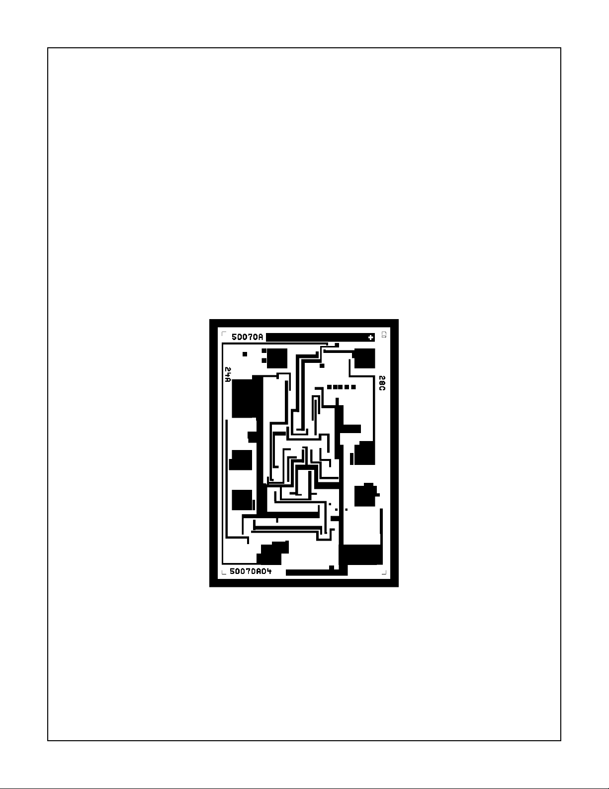
HFA1112/883
Die Characteristics
DIE DIMENSIONS:
63 x 44 x 19 mils ± 1 mils
1600µm x 1130µm x 483µm ± 25.4µm
METALLIZATION:
Type: Metal 1: AICu(2%)/TiW Type: Metal 2: AICu(2%)
Thickness: Metal 1: 8k
Å ± 0.4kÅ Thickness: Metal 2: 16kÅ ± 0.8kÅ
GLASSIVATION:
Type: Nitride
Thickness: 4k
WORST CASE CURRENT DENSITY:
2.0 x 10
Å ± 0.5kÅ
5
A/cm2at 47.5mA
TRANSISTOR COUNT: 52
SUBSTRATE POTENTIAL (Powered Up): Floating (Recommend Connection to V-)
Metallization Mask Layout
HFA1112/883
NC
NC
NC
+IN
V-
-IN
NC
V+
OUT
3-188
Spec Number 511084-883

HFA1112/883
Test Circuit
-V
IN
+V
IN
V
+I
BIAS
Z
=
100K
V
Z
(Applies to Table 1)
V+
0.1
100K (0.01%)
+
HA-5177
K2
K1
+
I
CC
NC
1
2
1
2
0.1
10 0.1
0.1
+
2
3
10 0.1
+
-
7
DUT
4
510
6
100 100
0.1
510
470pF
K3
1K
V
VOS =
+
x100
V
OUT
Y
100
V
Y
NOTE:
I
EE
1. All Resistors = ±1% (Ω)
2. All Capacitors = ±10% (µF)
V-
3. Unless Otherwise Noted
4. Chip Components Recommended
5. For AV = +1, K1 = Position 1, K2 = Position 1
6. For AV = +2, K1 = Position 1, K2 = Position 2, -VIN = 0V
7. For AV = -1, K1 = Position 1, K2 = Position 2, +VIN = 0V
Test Waveforms
SIMPLIFIED TEST CIRCUIT FOR LARGE AND SMALL SIGNAL PULSE RESPONSE (Applies to Table 3)
AV = +1 or +2 TEST CIRCUIT
V
IN
R
S
50Ω
NOTE:
1. VS = ±5V, RG = 0Ω for AV = +2, RG = ∞ for AV = +1
2. RF = Internal, RS = 50Ω
3. RL = 100Ω For Small and Large Signals
LARGE SIGNAL WAVEFORM
V
OUT
+2.5V
+SR
-2.5V -2.5V
10%
R
3
2
G
90%
V+
+
7
6
-
V-
50Ω
4
90%
10%
50Ω
V
-SR
OUT
2
+2.5V
AV = -1 TEST CIRCUIT
V+
7
2
V
IN
R
S
50Ω
6
-
3
+
4
V-
50Ω
50Ω
NOTE:
1. VS = ±5V, AV = -1
2. RF = Internal
3. RS = 50Ω, RL = 100Ω For Small and Large Signals
SMALL SIGNAL WAVEFORM
V
OUT
+250mV
TR, +OS
-250mV -250mV
10%
90%
90%
T
10%
V
OUT
2
+250mV
, -OS
F
3-189
Spec Number 511084-883
 Loading...