

Page 1
®
HFA1112
Data Sheet July 27, 2005
850MHz, Low Distortion Programmable
Gain Buffer Amplifiers
The HFA1112 is a closed loop Buffer featuring user
programmable gain and ultra high speed performance.
Manufactured on Intersil’s proprietary complementary
bipolar UHF-1 process, these devices offer a wide -3dB
bandwidth of 850MHz, very fast slew rate, excellent gain
flatness, low distortion and high output current.
A unique feature of the pinout allows the user to select a
voltage gain of +1, -1, or +2, without the use of any external
components. Gain selection is accomplished via
connections to the inputs, as described in the “Application
Information” section. The result is a more flexible product,
fewer part types in inventory, and more efficient use of board
space.
Compatibility with existing op amp pinouts provides flexibility
to upgrade low gain amplifiers, while decreasing component
count. Unlike most buffers, the standard pinout provides an
upgrade path should a higher closed loop gain be needed at
a future date.
This amplifier is available with programmable output limiting
as the HF A1113. For applications requiring a standard buffer
pinout, please refer to the HFA1110 data sheet.
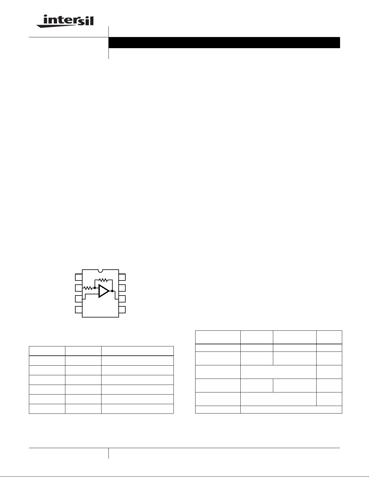
HFA1112 (PDIP, SOIC)
TOP VIEW
300
300
+
8
NC
V+
7
6
OUT
NC
5
NC
-IN
+IN
1
2
3
V-
4
FN2992.8
Features
• User Programmable for Closed-Loop Gains of +1, -1 or +2
without Use of External Resistors
• Wide -3dB Bandwidth. . . . . . . . . . . . . . . . . . . . . . 850MHz
• Very Fast Slew Rate. . . . . . . . . . . . . . . . . . . . . . 2400V/µs
• Fast Settling Time (0.1%). . . . . . . . . . . . . . . . . . . . . 11ns
• High Output Current. . . . . . . . . . . . . . . . . . . . . . . . . 60mA
• Excellent Gain Accuracy . . . . . . . . . . . . . . . . . . . 0.99V/V
• Overdrive Recovery . . . . . . . . . . . . . . . . . . . . . . . . <10ns
• Standard Operational Amplifier Pinout
• Pb-Free Plus Anneal Available (RoHS Compliant)
Applications
• RF/IF Processors
• Driving Flash A/D Converters
• High-Speed Communications
• Impedance Transformation
• Line Driving
• Video Switching and Routing
• Radar Systems
• Medical Imaging Systems
• Related Literature
- AN9507, Video Cable Drivers Save Board Space
Related Literature
• Technical Brief TB363 “Guidelines for Handling and
Processing Moisture Sensitive Surface Mount Devices
(SMDs)”
Pin Descriptions
NAME PIN NUMBER DESCRIPTION
NC 1, 5, 8 No Connection
-IN 2 Inverting Input
+IN 3 Non-Inverting Input
V- 4 Negative Supply
OUT 6 Output
V+ 7 Positive Supply
1
Ordering Information
PART NUMBER
(BRAND)
HFA1112IP -40 to 85 8 Ld PDIP E8.3
HFA1112IB
(1112IB)
HFA1112IB96
(1112IB)
HFA1112IBZ
(1112IBZ) (Note)
HFA1112IBZ96
(1112IBZ) (Note)
HFA11XXEVAL High Speed Op Amp DIP Evaluation Board
NOTE: Intersil Pb-free plus anneal products employ special Pb-free material sets;
molding compounds/die attach materials and 100% matte tin plate termination finish,
which are RoHS compliant and compatible with both SnPb and Pb-free soldering
operations. Intersil Pb-free products are MSL classified at Pb-free peak reflow
temperatures that meet or exceed the Pb-free requirements of IPC/JEDEC J STD-020.
CAUTION: These devices are sensitive to electrostatic discharge; follow proper IC Handling Procedures.
1-888-INTERSIL or 321-724-7143
| Intersil (and design) is a registered trademark of Intersil Americas Inc.
Copyright Intersil Americas Inc. 2000 2004, 2005. All Rights Reserved
All other trademarks mentioned are the property of their respective owners.
TEMP.
RANGE (°C) PACKAGE
-40 to 85 8 Ld SOIC M8.15
8 Ld SOIC Tape and Reel M8.15
-40 to 85 8 Ld SOIC
(Pb-free)
8 Ld SOIC Tape and Reel
(Pb-free)
PKG.
DWG. #
M8.15
M8.15
Page 2
HFA1112
Absolute Maximum Ratings Thermal Information
Voltage Between V+ and V-. . . . . . . . . . . . . . . . . . . . . . . . . . . . .12V
Input Voltage . . . . . . . . . . . . . . . . . . . . . . . . . . . . . . . . . . . V
Output Current. . . . . . . . . . . . . . . . . . . . . . . . . . . . . . . . . . . . . 60mA
SUPPLY
Thermal Resistance (Typical, Note 1) θ
PDIP Package . . . . . . . . . . . . . . . . . . . 125 N/A
SOIC Package . . . . . . . . . . . . . . . . . . . 170 N/A
Maximum Junction Temperature (Plastic Package) . . . . . . . .150
Operating Conditions
Temperature Range . . . . . . . . . . . . . . . . . . . . . . . . . . -40oC to 85oC
CAUTION: Stresses above those listed in “Absolute Maximum Ratings” may cause permanent damage to the device. This is a stress only rating and operation of the
device at these or any other conditions above those indicated in the operational sections of this specificat ion is not implied.
Maximum Storage Temperature Range. . . . . . . . . . -65
Maximum Lead Temperature (Soldering 10s) . . . . . . . . . . . . 300
(SOIC - Lead Tips Only)
NOTE:
is measured with the component mounted on a low effective thermal conductivity test board in free air. See Tech Brief TB379 for details.
1. θ
JA
(oC/W) θJC (oC/W)
JA
o
C to 150oC
o
o
C
C
Electrical Specifications V
PARAMETER TEST CONDITIONS TEMP (
= ±5V, AV = +1, RL = 100Ω, Unless Otherwise Specified
SUPPLY
o
C) MIN TYP MAX UNITS
INPUT CHARACTERISTICS
Output Offset Voltage 25 - 8 25 mV
Full - - 35 mV
Output Offset Voltage Drift Full - 10 - µV/
PSRR 25 39 45 - dB
Full 35 - - dB
Input Noise Voltage (Note 3) 100kHz 25 - 9 - nV/√Hz
Non-Inv erting Input N o ise Cu rrent (Not e 3) 100kHz 25 - 37 - pA/√Hz
Non-Inverting Input Bias Current 25 - 25 40 µA
Full - - 65 µA
Non-Inverting Input Resistance 25 25 50 - kΩ
Inverting Input Resistance (Note 2) 25 240 300 360 Ω
Input Capacitance 25 - 2 - pF
Input Common Mode Range Full ±2.5 ±2.8 - V
TRANSFER CHARACTERISTICS
Gain A
= +1, VIN = +2V 25 0.980 0.990 1.02 V/V
V
Full 0.975 - 1.025 V/V
Gain A
= +2, VIN = +1V 25 1.96 1.98 2.04 V/V
V
Full 1.95 - 2.05 V/V
DC Non-Linearity (Note 3) A
= +2, ±2V Full Scale 25 - 0.02 - %
V
OUTPUT CHARACTERISTICS
Output Voltage (Note 3) A
= -1 25 ±3.0 ±3.3 - V
V
Full ±2.5 ±3.0 - V
Output Current (Note 3) R
= 50Ω 25, 85 50 60 - mA
L
-40 35 50 - mA
Closed Loop Output Impedance DC, A
= +2 25 - 0.3 - Ω
V
POWER SUPPLY CHARACTERISTICS
Supply Voltage Range Full ±4.5 - ±5.5 V
Supply Current (Note 3) 25 - 21 26 mA
Full - - 33 mA
AC CHARACTERISTICS
= -1 25 450 800 - MHz
-3dB Bandwidth
= 0.2V
(V
OUT
, Notes 2, 3)
P-P
A
V
A
= +1 25 500 850 - MHz
V
= +2 25 350 550 - MHz
A
V
o
C
2
Page 3
HFA1112
Electrical Specifications V
PARAMETER TEST CONDITIONS TEMP (
Slew Rate
(V
= 5V
OUT
Full Power Bandwidth
(V
= 5V
OUT
Gain Flatness
(to 30MHz, Notes 2, 3)
Gain Flatness
(to 50MHz, Notes 2, 3)
Gain Flatness
(to 100MHz, Notes 2, 3)
Linear Phase Deviation
(to 100MHz, Note 3)
2nd Harmonic Distortion
(30MHz, V
3rd Harmonic Distortion
(30MHz, V
2nd Harmonic Distortion
(50MHz, V
3rd Harmonic Distortion
(50MHz, V
2nd Harmonic Distortion
(100MHz, V
3rd Harmonic Distortion
(100MHz, V
3rd Order Intercept
(A
= +2, Note 3)
V
1dB Compression
= +2, Note 3)
(A
V
Reverse Isolation
, Note 3)
(S
12
TRANSIENT CHARACTERISTICS
Rise Time
= 0.5V Step, Note 2)
(V
OUT
P-P
P-P
OUT
OUT
OUT
OUT
OUT
OUT
, Note 2)
, Note 3)
= 2V
P-P
= 2V
P-P
= 2V
P-P
= 2V
P-P
= 2V
= 2V
, Notes 2, 3)
, Notes 2, 3)
, Notes 2, 3)
, Notes 2, 3)
, Notes 2, 3)
P-P
, Notes 2, 3)
P-P
= ±5V, AV = +1, RL = 100Ω, Unless Otherwise Specified (Continued)
SUPPLY
o
C) MIN TYP MAX UNITS
= -1 25 1500 2400 - V/µs
A
V
= +1 25 800 1500 - V/µs
A
V
= +2 25 1100 1900 - V/µs
A
V
= -1 25 - 300 - MHz
A
V
A
= +1 25 - 150 - MHz
V
= +2 25 - 220 - MHz
A
V
= -1 25 - ±0.02 - dB
A
V
= +1 25 - ±0.1 - dB
A
V
= +2 25 - ±0.015 ±0.04 dB
A
V
= -1 25 - ±0.05 - dB
A
V
= +1 25 - ±0.2 - dB
A
V
= +2 25 - ±0.036 ±0.08 dB
A
V
= -1 25 - ±0.10 - dB
A
V
= +2 25 - ±0.07 ±0.22 dB
A
V
= -1 25 - ±0.13 - Degrees
A
V
= +1 25 - ±0.83 - Degrees
A
V
= +2 25 - ±0.05 - Degrees
A
V
= -1 25 - -52 - dBc
A
V
= +1 25 - -57 - dBc
A
V
= +2 25 - -52 -45 dBc
A
V
= -1 25 - -71 - dBc
A
V
= +1 25 - -73 - dBc
A
V
= +2 25 - -72 -65 dBc
A
V
= -1 25 - -47 - dBc
A
V
= +1 25 - -53 - dBc
A
V
= +2 25 - -47 -40 dBc
A
V
= -1 25 - -63 - dBc
A
V
= +1 25 - -68 - dBc
A
V
= +2 25 - -65 -55 dBc
A
V
= -1 25 - -41 - dBc
A
V
A
= +1 25 - -50 - dBc
V
= +2 25 - -42 -35 dBc
A
V
= -1 25 - -55 - dBc
A
V
A
= +1 25 - -49 - dBc
V
= +2 25 - -62 -45 dBc
A
V
100MHz 25 - 28 - dBm
300MHz 25 - 13 - dBm
100MHz 25 - 19 - dBm
300MHz 25 - 12 - dBm
40MHz 25 - -70 - dB
100MHz 25 - -60 - dB
600MHz 25 - -32 - dB
= -1 25 - 500 800 ps
A
V
= +1 25 - 480 750 ps
A
V
A
= +2 25 - 700 1000 ps
V
3
Page 4

HFA1112
Electrical Specifications V
PARAMETER TEST CONDITIONS TEMP (
Rise Time
(V
= 2V Step)
OUT
Overshoot
(V
= 0.5V Step, Input tR/tF = 200ps,
OUT
Notes 2, 3, 4)
0.1% Settling Time (Note 3) V
0.05% Settling Time V
Overdrive Recovery Time V
Differential Gain A
Differential Phase A
NOTES:
2. This parameter is not tested. The limits are guaranteed based on lab characterization, and reflect lot-to-lot variation.
3. See Typical Performance Curves for more information.
4. Overshoot decreases as input transition times increase, especially for A
Application Information
= ±5V, AV = +1, RL = 100Ω, Unless Otherwise Specified (Continued)
SUPPLY
o
C) MIN TYP MAX UNITS
= -1 25 - 0.82 - ns
A
V
= +1 25 - 1.06 - ns
A
V
= +2 25 - 1.00 - ns
A
V
A
= -1 25 - 12 30 %
V
A
= +1 25 - 45 65 %
V
= +2 25 - 6 20 %
A
V
= 2V to 0V 25 - 11 - ns
OUT
= 2V to 0V 25 - 15 - ns
OUT
= 5V
IN
P-P
= +1, 3.58MHz, RL = 150Ω 25 - 0.03 - %
V
= +2, 3.58MHz, RL = 150Ω 25 - 0.02 - %
A
V
= +1, 3.58MHz, RL = 150Ω 25 - 0.05 - Degrees
V
= +2, 3.58MHz, RL = 150Ω 25 - 0.04 - Degrees
A
V
25 - 8.5 - ns
= +1. Please refer to Typical Performance Curves.
V
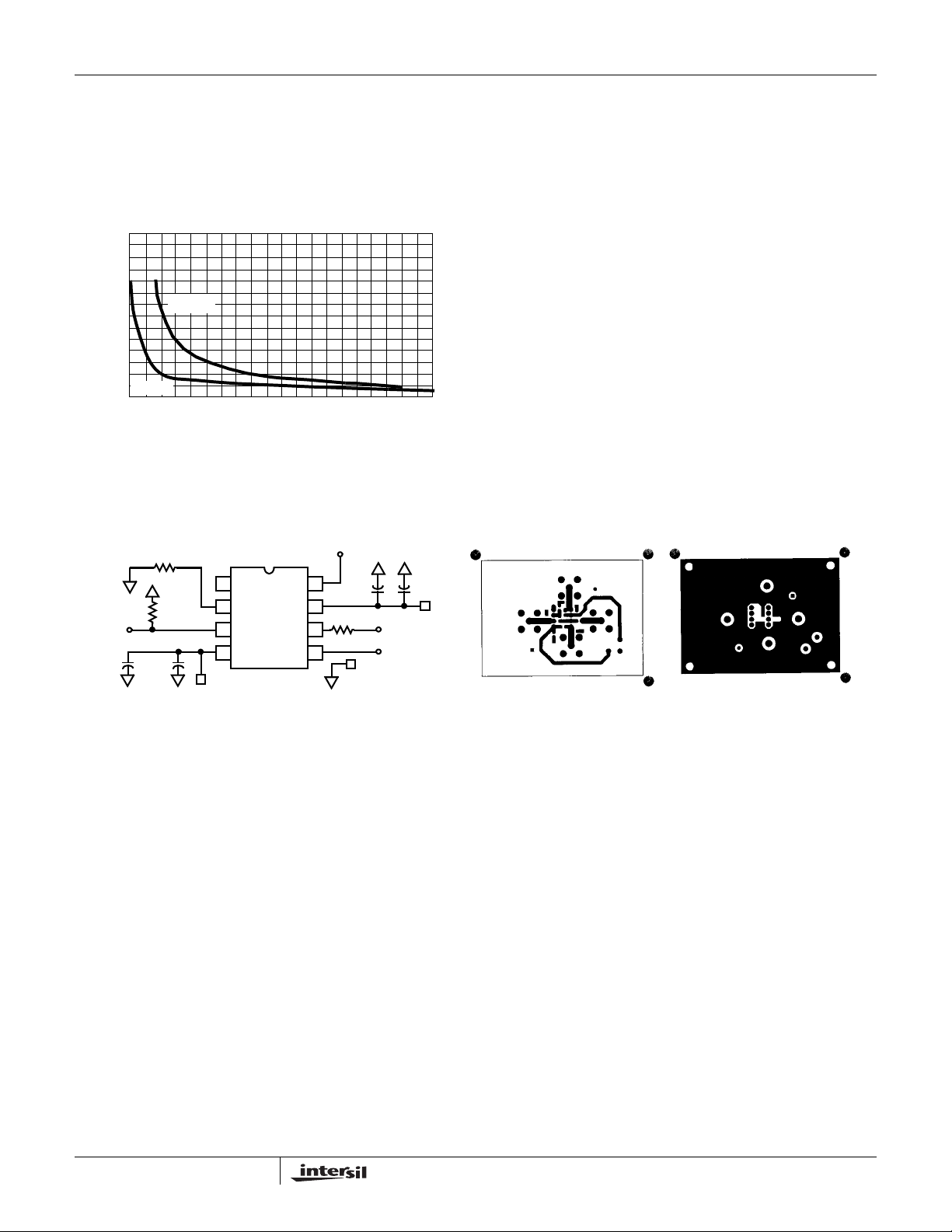
Terminated microstrip signal lines are recommended at the
input and output of the device. Capacitance directly on the
Closed Loop Gain Selection
The HFA1112 features a novel design which allows the user
to select from three closed loop gains, without any external
components. The result is a more flexible product, fewer part
types in inventory, and more efficient use of board space.
This “buffer” operates in closed loop gains of -1, +1, or +2, and
gain selection is accomplished via connections to the ±inputs.
Applying the input signal to +IN and floating -IN selects a gain
of +1, while grounding -IN selects a gain of +2. A gain of -1 is
obtained by applying the input signal to -IN with +IN grounded.
The table below summarizes these connections:
output must be minimized, or isolated as discussed in the
next section.
For unity gain applications, care must also be taken to
minimize the capacitance to ground seen by the amplifier’s
inverting input. At higher frequencies this capacitance will
tend to short the -INPUT to GND, resulting in a closed loop
gain which increases with frequency. This will cause
excessive high frequency peaking and potentially other
problems as well.
An example of a good high frequency layout is the
Evaluation Board shown in Figure 2.
GAIN
(A
)
CL
-1 GND Input
+1 Input NC (Floating)
+2 Input GND
+INPUT (PIN 3) -INPUT (PIN 2)
CONNECTIONS
PC Board Layout
The frequency response of this amplifier depends greatly on
the amount of care taken in designing the PC board. The
use of low inductance components such as chip
resistors and ch ip cap acito r s is strongly recomm ended ,
while a solid ground plane is a must!
Attention should be given to decoupling the power supplies.
A large value (10µF) tantalum in parallel with a small value
(0.1µF) chip capacitor works well in most cases.
4
Driving Capacitive Loads
Capacitive loads, such as an A/D input, or an improperly
terminated transmission line will degrade the amplifier’s
phase margin resulting in frequency response peaking and
possible oscillations. In most cases, the oscillation can be
avoided by placing a resistor (R
prior to the capacitance.
Figure 1 details starting points for the selection of this
resistor. The points on the curve indicate the R
combinations for the optimum bandwidth, stability, and
settling time, but experimental fine tuning is recommended.
Picking a point above or to the right of the curve yields an
overdamped response, while points below or left of the curve
indicate areas of underdamped performance.
R
and CL form a low pass network at the output, thus
S
limiting system bandwidth well below the amplifier
bandwidth of 850MHz. By decreasing R
) in series with the output
S
and CL
S
as CLincreases
S
Page 5
HFA1112
(as illustrated in the curves), the maximum bandwidth is
obtained without sacrificing stability. Even so, bandwidth
does decrease as you move to the right along the curve.
For example , at A
= +1, RS = 50Ω, CL = 30pF, the overall
V
bandwidth is limited to 300MHz, and bandwidth drops to
100MHz at A
50
45
40
35
30
(Ω)
25
S
20
R
15
10
5
0
FIGURE 1. RECOMMENDED SERIES OUTPUT RESISTOR vs
IN
10µF
= +1, RS = 5Ω, CL = 340pF.
V
AV = +1
AV = +2
0 40 80 120 160 200 240 280 320 360 400
LOAD CAPACITANCE (pF)
LOAD CAPACITANCE
∞ (AV = +1)
or 0Ω (A
R
0.1µF
1
50Ω
= +2)
V
-5V
V
H
1
2
3
4
GND
8
7
50Ω
6
5
GND
OUT
V
L
10µF0.1µF
+5V
Evaluation Board
The performance of the HFA1112 may be evaluated using
the HFA11XX Evaluation Board, slightly modified as follows:
1. Remo ve the 500Ω f eedbac k resistor (R
connection open.
2. a. F or AV = +1 evaluation, remove the 500Ω gain setting
resistor (R1), and leave pin 2 floating.
b. For A
= +2, replace the 500Ω gain setting resistor with
V
a 0Ω resistor to GND.
The layout and modified schematic of the board are shown in
Figure 2.
To order evaluation boards (part number HFA11XXEVAL),
please contact your local sales office.
TOP LAYOUT BOTTOM LAYOUT
V
H
1
+IN
OUT
V+
V
L
V-
GND
), and leav e the
2
FIGURE 2. EVALUATION BOARD SCHEMATIC AND LAYOUT
5
Page 6

HFA1112
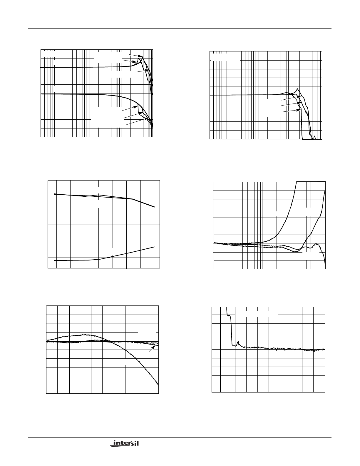
Typical Performance Curves V
200
AV = +2
150
100
50
0
-50
OUTPUT VOLTAGE (mV)
-100
-150
-200
TIME (5ns/DIV.)
FIGURE 3. SMALL SIGNAL PULSE RESPONSE FIGURE 4. LARGE SIGNAL PULSE RESPONSE
200
AV = +1
150
100
= ±5V, TA = 25oC, RL = 100Ω, Unless Otherwise Specified
SUPPLY
2.0
AV = +2
1.5
1.0
0.5
0
-0.5
OUTPUT VOLTAGE (V)
-1.0
-1.5
-2.0
2.0
A
= +1
V
1.5
1.0
TIME (5ns/DIV.)
OUTPUT VOLTAGE (mV)
50
0
-50
-100
-150
-200
TIME (5ns/DIV.)
OUTPUT VOLTAGE (V)
0.5
0
-0.5
-1.0
-1.5
-2.0
TIME (5ns/DIV.)
FIGURE 5. SMALL SIGNAL PULSE RESPONSE FIGURE 6. LARGE SIGNAL PULSE RESPONSE
OUTPUT VOLTAGE (mV)
200
150
100
-50
-100
AV = -1
50
0
2.0
AV = -1
1.5
1.0
0.5
0
-0.5
OUTPUT VOLTAGE (V)
-1.0
-150
-200
TIME (5ns/DIV.)
-1.5
-2.0
TIME (5ns/DIV.)
FIGURE 7. SMALL SIGNAL PULSE RESPONSE FIGURE 8. LARGE SIGNAL PULSE RESPONSE
6
Page 7

Page 8
HFA1112
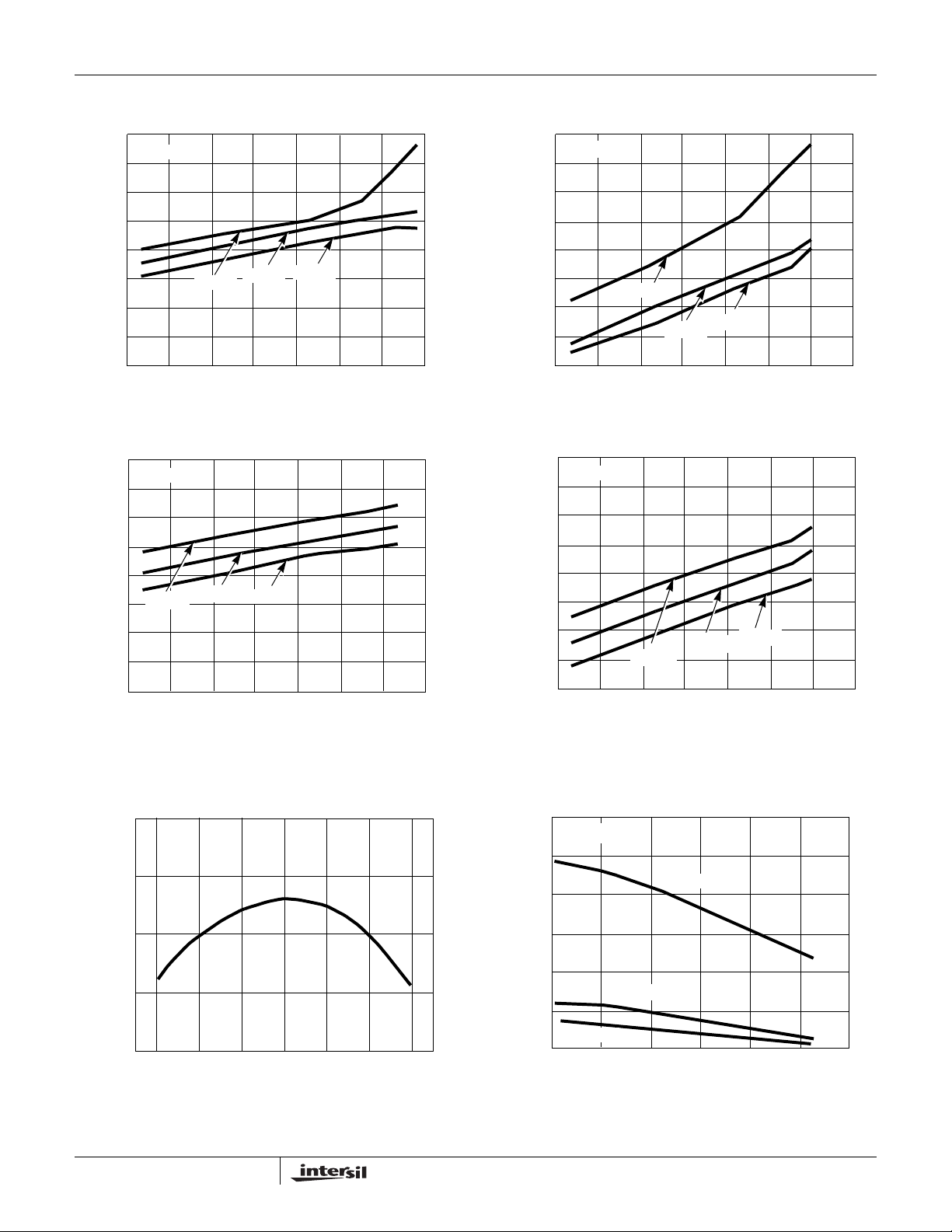
Typical Performance Curves V
6
AV = -1
3
GAIN
0
-3
GAIN (dB)
-6
PHASE
0.3 1 10 100 1000
FREQUENCY (MHz)
V
V
OUT
V
V
OUT
OUT
V
OUT
OUT
= 4V
= 2.5V
= 2.5V
= 4V
V
OUT
P-P
= 1V
P-P
= 1V
P-P
P-P
P-P
P-P
= ±5V, TA = 25oC, RL = 100Ω, Unless Otherwise Specified (Continued)
SUPPLY
180
90
0
-90
-180
FIGURE 15. FREQUENCY RESPONSE FOR VARIOUS OUTPUT
VOLTAGES
900
850
800
750
700
650
BANDWIDTH (MHz)
600
550
500
-50 -25 0 25 50 75 100 125
AV = +1
AV = -1
AV = +2
TEMPERATURE (
o
C)
PHASE (DEGREES)
15
V
= 5V
OUT
12
9
6
3
0
-3
-6
NORMALIZED GAIN (dB)
-9
-12
-15
0.3 1 10 100 1000
P-P
AV = -1
AV = +2
AV = +1
FREQUENCY (MHz)
FIGURE 16. FULL POWER BANDWIDTH
0.35
0.30
0.25
0.20
0.15
0.10
0.05
0
NORMALIZED GAIN (dB)
-0.05
-0.10
-0.15
1 10 100
FREQUENCY (MHz)
AV = +1
AV = -1
AV = +2
FIGURE 17. -3dB BANDWIDTH vs TEMPERATURE FIGURE 18. GAIN FLATNESS
4
3
2
1
0
-1
-2
-3
DEVIATION (DEGREES)
-4
-5
-6
0 15 30 45 60 75 90 105 120 135
FREQUENCY (MHz)
AV = +1
AV = -1
= +2
A
V
150
AV = +2, V
0.6
0.4
0.2
0.1
0
-0.1
-0.2
-0.4
SETTLING ERROR (%)
-0.6
-2 3 8 13 18 23 28 33 38 43 48
= 2V
OUT
TIME (ns)
FIGURE 19. DEVIATION FROM LINEAR PHASE FIGURE 20. SETTLING RESPONSE
8
Page 9

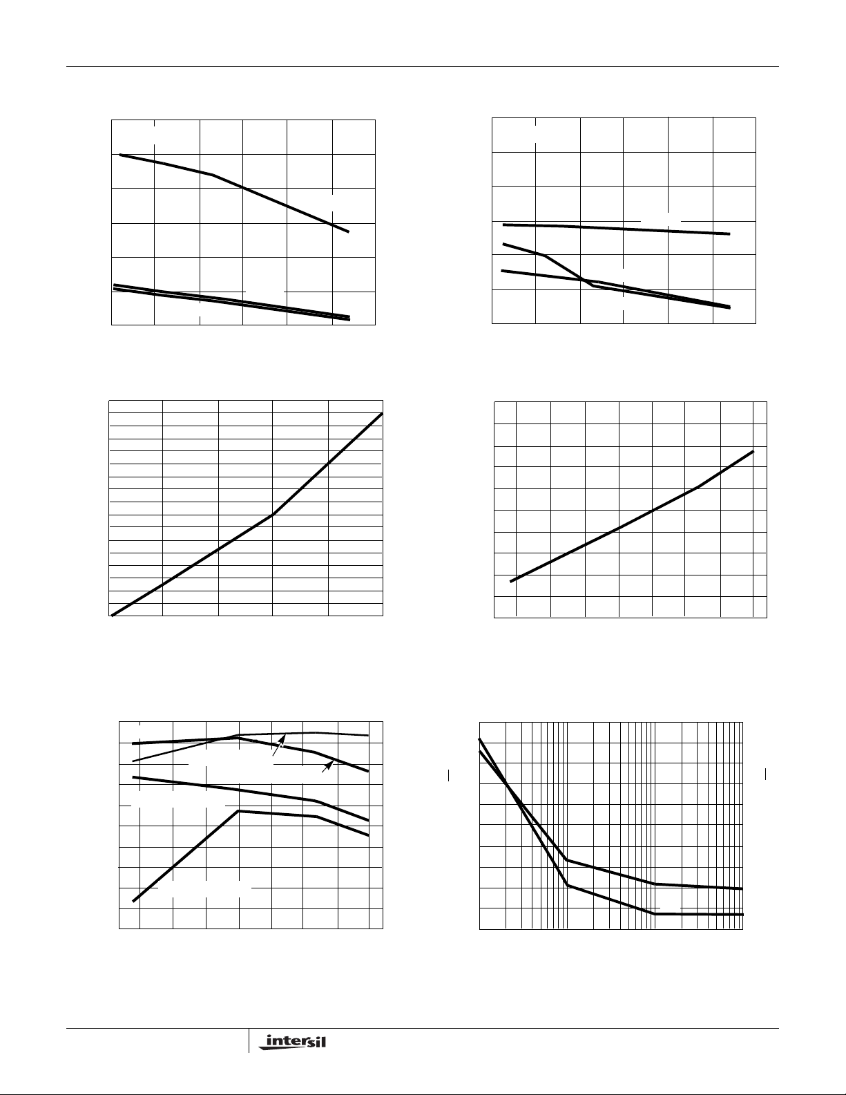
Typical Performance Curves V
= ±5V, TA = 25oC, RL = 100Ω, Unless Otherwise Specified (Continued)
SUPPLY
-24
-30
-36
-42
-48
-54
GAIN (dB)
-60
-66
-72
-78
-84
AV = -1
AV = +2
20 40 60 80 100 120 140 160 180 200
0
FREQUENCY (MHz)
AV = +1
AV = +2
AV = -1
AV = -1
-24
-30
-36
-42
-48
GAIN (dB)
-54
-60
100 190 280 370 460 550 640 730 820 910 1000
PHASE
AV = +2
= -1
A
V
FREQUENCY (MHz)
AV = +2
GAIN
AV = +1
AV = +1
235
180
90
45
0
FIGURE 21. LOW FREQUENCY REVERSE ISOLATION (S12) FIGURE 22. HIGH FREQUENCY REVERSE ISOLATION (S12)
20
18
16
14
12
10
8
6
4
2
0
OUTPUT POWER AT 1dB COMPRESSION (dBm)
100 200 300 400 500
AV = +1
AV = -1
AV = +2
FREQUENCY (MHz)
30
20
10
INTERCEPT POINT (dBm)
0
100 200 300 400
2 - TONE
AV = -1
AV = +2
AV = +1
FREQUENCY (MHz)
PHASE (DEGREES)
FIGURE 23. 1dB GAIN COMPRESSION vs FREQUENCY FIGURE 24. 3rd ORDER INTERMODULATION INTERCEPT vs
FREQUENCY
-20
-30
-40
-50
-60
-70
DISTORTION (dBc)
-80
-90
-100
-6 -3 0 3 6 9 12 15
OUTPUT POWER (dBm)
FIGURE 25. 2nd HARMONIC DISTORTION vs P
OUT
FIGURE 26. 3rd HARMONIC DISTORTION vs P
OUT
9
Page 10
HFA1112
Typical Performance Curves V
-20
AV = +1
-30
-40
-50
-60
-70
DISTORTION (dBc)
-80
-90
-100
-6 -3 0 3 6 9 12 15
100MHz
50MHz
OUTPUT POWER (dBm)
FIGURE 27. 2nd HARMONIC DISTORTION vs P
DISTORTION (dBc)
-100
-20
-30
-40
-50
-60
-70
-80
-90
AV = -1
100MHz
-6 -3 0 3 6 9 12 15
50MHz
OUTPUT POWER (dBm)
30MHz
30MHz
= ±5V, TA = 25oC, RL = 100Ω, Unless Otherwise Specified (Continued)
SUPPLY
-20
AV = +1
-30
-40
-50
-60
OUT
-70
DISTORTION (dBc)
-80
-90
-100
-6 -3 0 3 6 9 12 15
FIGURE 28. 3rd HARMONIC DISTORTION vs P
-20
AV = -1
-30
-40
-50
-60
-70
DISTORTION (dBc)
-80
-90
-100
-6 -3 0 3 6 9 12 15
100MHz
50MHz
OUTPUT POWER (dBm)
50MHz
100MHz
OUTPUT POWER (dBm)
30MHz
OUT
30MHz
FIGURE 29. 2nd HARMONIC DISTORTION vs P
0.04
0.02
0
PERCENT ERROR (%)
-0.02
-0.04
-3.0
-2.0 -1.0 0 1.0 2.0 3.0
INPUT VOLTAGE (V)
OUT
FIGURE 30. 3rd HARMONIC DISTORTION vs P
60
V
= 0.5V
OUT
50
40
30
20
OVERSHOOT (%)
AV = -1
10
AV = +2
0
100 300 500 700 900 1100 1300
AV = +1
INPUT RISE TIME (ps)
FIGURE 31. INTEGRAL LINEARITY ERROR FIGURE 32. OVERSHOOT vs INPUT RISE TIME
10
OUT
Page 11
HFA1112
Typical Performance Curves V
60
V
= 1V
OUT
50
40
30
20
OVERSHOOT (%)
10
AV = +2
0
100 300 500 700 900 1100 1300
INPUT RISE TIME (ps)
AV = -1
= ±5V, TA = 25oC, RL = 100Ω, Unless Otherwise Specified (Continued)
SUPPLY
60
V
= 2V
OUT
50
40
AV = +1
30
20
OVERSHOOT (%)
10
AV = -1
0
100 300 500 700 900 1100 1300
INPUT RISE TIME (ps)
AV = +1
AV = +2
FIGURE 33. OVERSHOOT vs INPUT RISE TIME FIGURE 34. OVERSHOOT vs INPUT RISE TIME
22
21
20
19
18
17
16
15
14
13
12
11
10
SUPPLY CURRENT (mA)
9
8
7
6
5
59
678 10
TOTAL SUPPLY VOLTAGE (V+ - V-, V)
25
24
23
22
21
20
19
18
SUPPLY CURRENT (mA)
17
16
15
-50 -25 0 25 50 75 100 125
TEMPERATURE (
o
C)
FIGURE 35. SUPPLY CURRENT vs SUPPLY VOLTAGE FIGURE 36. SUPPLY CURRENT vs TEMPERATURE
OUTPUT VOLTAGE (V)
3.6
AV = -1
3.5
+V
(RL= 50Ω)
3.4
3.3
|-V
3.2
3.1
3.0
2.9
2.8
2.7
2.6
OUT
-50 -25 0 25 50 75 100 125
OUT
| (RL= 100Ω)
|-V
| (RL= 50Ω)
OUT
TEMPERATURE (
+V
OUT
(RL= 100Ω)
o
C)
50
40
30
20
E
NOISE VOLTAGE (nV/√Hz)
10
0
0.1 1 10 100
FREQUENCY (kHz)
NI
I
NI
FIGURE 37. OUTPUT VOLTAGE vs TEMPERATURE FIGURE 38. INPUT NOISE CHARACTERISTICS
11
130
110
90
70
50
30
NOISE CURRENT (pA/√Hz)
Page 12
Die Characteristics
HFA1112
DIE DIMENSIONS
63 mils x 44 mils x 19 mils
1600µm x 1130µm 483µm
METALLIZATION
Type: Metal 1: AlCu (2%)/TiW
Thickness: Metal 1: 8kÅ ±0.4kÅ
Type: Metal 2: AlCu (2%)
Thickness: Metal 2: 16k
Å ±0.8kÅ
Metallization Mask Layouts
HFA1112
NC
V-
PASSIVATION
Type: Nitride
Thickness: 4kÅ ±0.5kÅ
TRANSISTOR COUNT
52
SUBSTRATE POTENTIAL (POWERED UP)
Floating (Recommend Connection to V-)
+IN
NC
NC
-IN
NC
V+
OUT
12
Page 13

Dual-In-Line Plastic Packages (PDIP)
HFA1112
N
D1
-C-
E1
-B-
A2
A
L
A
1
e
C
e
e
INDEX
AREA
BASE
PLANE
SEATING
PLANE
D1
B1
12 3 N/2
-AD
e
B
0.010 (0.25) C AM BS
NOTES:
1. Controlling Dimensions: INCH. In case of conflict between
English and Metric dimensions, the inch dimensions control.
2. Dimensioning and tolerancing per ANSI Y14.5M-1982.
3. Symbols are defined in the “MO Series Symbol List” in Section
2.2 of Publication No. 95.
4. Dimensions A, A1 and L are measured with the package seated
in JEDEC seating plane gauge GS-3.
5. D, D1, and E1 dimensions do not include mold flash or protrusions. Mold flash or protrusions shall not exceed 0.010 inch
(0.25mm).
6. E and are measured with the leads constrained to be per-
7. e
e
pendicular to datum .
A
and eC are measured at the lead tips with the leads uncon-
B
strained. e
must be zero or greater.
C
-C-
8. B1 maximum dimensions do not include dambar protrusions.
Dambar protrusions shall not exceed 0.010 inch (0.25mm).
9. N is the maximum number of terminal positions.
10. Corner leads (1, N, N/2 and N/2 + 1) for E8.3, E16.3, E18.3,
E28.3, E42.6 will have a B1 dimension of 0.030 - 0.045 inch
(0.76 - 1.14mm).
E8.3 (JEDEC MS-001-BA ISSUE D)
8 LEAD DUAL-IN-LINE PLASTIC PACKAGE
INCHES MILLIMETERS
SYMBOL
A - 0.210 - 5.33 4
E
A1 0.015 - 0.39 - 4
A2 0.115 0.195 2.93 4.95 -
B 0.014 0.022 0.356 0.558 -
C
L
A
C
B
B1 0.045 0.070 1.15 1.77 8, 10
C 0.008 0.014 0.204 0.355 D 0.355 0.400 9.01 10.16 5
D1 0.005 - 0.13 - 5
E 0.300 0.325 7.62 8.25 6
E1 0.240 0.280 6.10 7.11 5
e 0.100 BSC 2.54 BSC -
e
A
e
B
0.300 BSC 7.62 BSC 6
- 0.430 - 10.92 7
L 0.115 0.150 2.93 3.81 4
N8 89
NOTESMIN MAX MIN MAX
Rev. 0 12/93
13
Page 14

Small Outline Plastic Packages (SOIC)
HFA1112
N
INDEX
AREA
123
-A-
E
-B-
SEATING PLANE
D
A
-C-
0.25(0.010) BM M
H
L
h x 45°
α
e
B
0.25(0.010) C AM BS
M
NOTES:
1. Symbols are defined in the “MO Series Symbol List” in Section 2.2 of
Publication Number 95.
2. Dimensioning and tolerancing per ANSI Y14.5M-1982.
3. Dimension “D” does not include mold flash, protrusions or gate burrs.
Mold flash, protrusion and gate burrs shall not exceed 0.15mm (0.006
inch) per side.
4. Dimension “E” does not include interlead flash or protrusions. Interlead flash and protrusions shall not exceed 0.25mm (0.010 inch) per
side.
5. The chamfer on the body is optional. If it is not present, a visual index
feature must be located within the crosshatched area.
6. “L” is the length of terminal for soldering to a substrate.
7. “N” is the number of terminal positions.
8. Terminal numbers are shown for reference only.
9. The lead width “B”, as measured 0.36mm (0.014 inch) or greater
above the seating plane, shall not exceed a maximum value of
0.61mm (0.024 inch).
10. Controlling dimension: MILLIMETER. Converted inch dimensions
are not necessarily exact.
A1
C
0.10(0.004)
M8.15 (JEDEC MS-012-AA ISSUE C)
8 LEAD NARROW BODY SMALL OUTLINE PLASTIC PACKAGE
INCHES MILLIMETERS
SYMBOL
A 0.0532 0.0688 1.35 1.75 -
A1 0.0040 0.0098 0.10 0.25 -
B 0.013 0.020 0.33 0.51 9
C 0.0075 0.0098 0.19 0.25 D 0.1890 0.1968 4.80 5.00 3
E 0.1497 0.1574 3.80 4.00 4
e 0.050 BSC 1.27 BSC H 0.2284 0.2440 5.80 6.20 h 0.0099 0.0196 0.25 0.50 5
L 0.016 0.050 0.40 1.27 6
N8 87
α
0° 8° 0° 8° -
NOTESMIN MAX MIN MAX
Rev. 1 6/05
All Intersil U.S. products are manufactured, assembled and tested utilizing ISO9000 quality systems.
Intersil Corporation’s quality certifications can be viewed at www.intersil.com/design/quality
Intersil products are sold by description only. Intersil Corporation reserves the right to make changes in circuit design, software and/or specifications at any time without
notice. Accordingly, the reader is cautioned to verify that data sheets are current before placing orders. Information furnished by Intersil is believed to be accurate and
reliable. However, no responsibility is assumed by Intersil or its subsidiaries for its use; nor for any infringements of patents or other rights of third parties which may result
from its use. No license is granted by implication or otherwise under any patent or patent rights of Intersil or its subsidiaries.
For information regarding Intersil Corporation and its products, see www.intersil.com
14
 Loading...