November 1998
HFA1110/883
750MHz, Low Distortion
Unity Gain, Closed Loop Buffer
Features
• This Circuit is Processed in Accordance to MIL-STD883 and is Fully Conformant Under the Provisions of
Paragraph 1.2.1.
• Fixed Gain of +1
• Wide -3dB Bandwidth . . . . . . . . . . . . . . . 750MHz (Typ)
• Very Fast Slew Rate. . . . . . . . . . . . . . . . 1250V/µs (Typ)
• Low Differential Gain and Phase . . . 0.04%/0.025 Deg.
• Low Distortion (HD3, 30MHz) . . . . . . . . . . -80dBc (Typ)
• Excellent Gain Flatness (to 100MHz) . . . ±0.03dB (Typ)
• Excellent Gain Accuracy. . . . . . . . . . . . . .0.99V/V (Typ)
• High Output Current . . . . . . . . . . . . . . . . . . 60mA (Typ)
Applications
• Video Switching and Routing
• Pulse and Video Amplifiers
• Wideband Amplifiers
• RF/IF Signal Processing
• Flash A/D Driver
Description
The HFA1110/883 is a unity gain, closed loop buffer which
achieves a high degree of gain accuracy, wide bandwidth,
and low distortion. Manufactured on Intersil’s proprietary
complementary bipolar UHF-1 process, the HFA1110/883
also offers very fast slew rates, and high output current.
Component and composite video systems will also benefit
from this buffer’s performance, as indicated by the excellent
gain flatness, and 0.04%/0.025 Degree Differential
Gain/Phase specifications (R
For buffer applications desiring a standard op amp pinout, or
selectable gain (-1, +1, +2), please refer to the HFA1112/883
and HFA1113/883 (featuring programmable output clamps)
datasheets.
= 75Ω).
L
Ordering Information
TEMP.
PART NUMBER
HFA1110MJ/883 -55 to 125 8 Ld CERDIP F8.3A
RANGE (oC) PACKAGE PKG. NO.
• Medical Imaging Systems
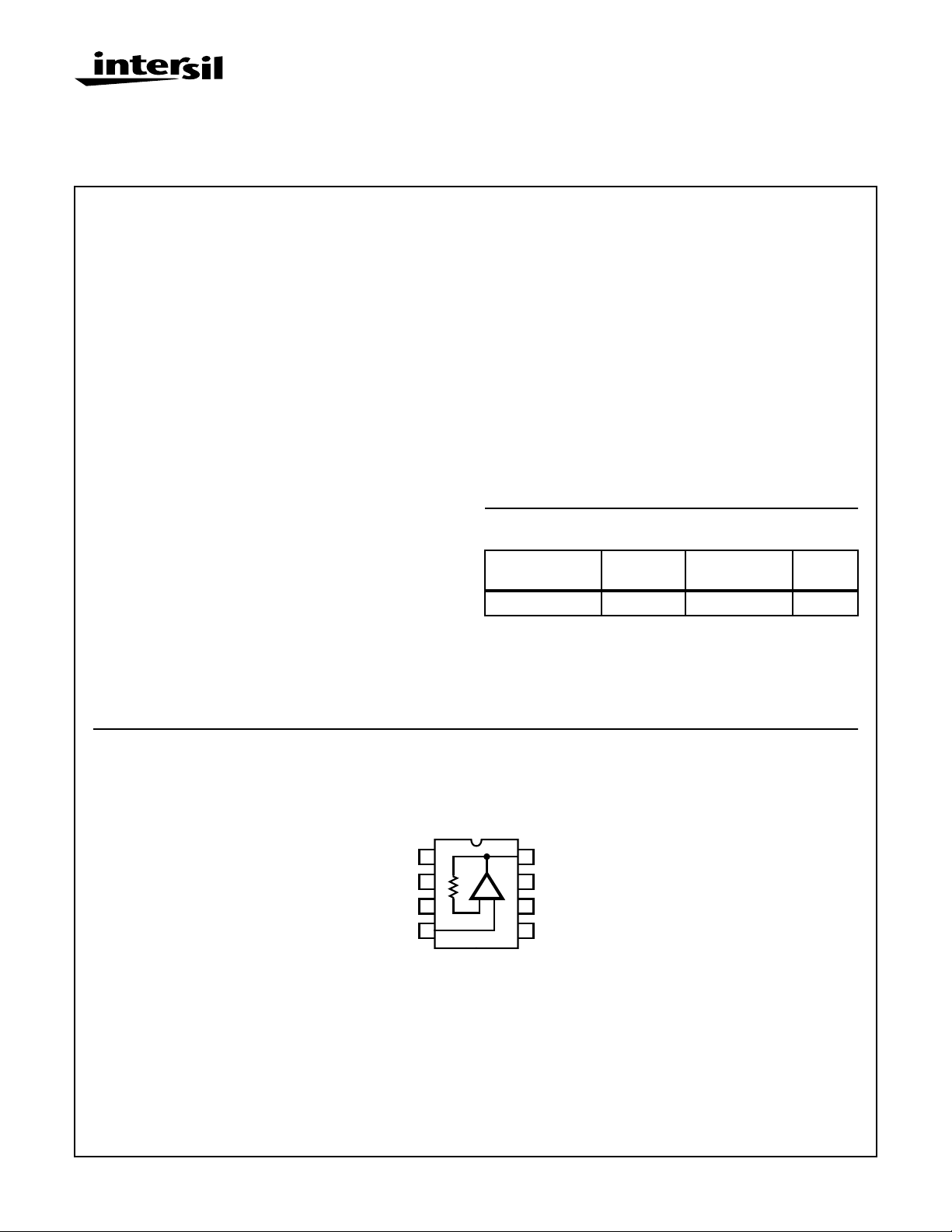
Pinout
V+
OPT V+
NC
1
2
3
4
IN
HFA1110/883
(CERDIP)
TOP VIEW
+
-
8
7
6
5
OUT
NC
OPT VV-
CAUTION: These devices are sensitive to electrostatic discharge; follow proper IC Handling Procedures.
1-888-INTERSIL or 321-724-7143
| Copyright © Intersil Corporation 1999
1
Spec Number
File Number 3620.2
511083-883

HFA1110/883
Absolute Maximum Ratings Thermal Information
Voltage Between V+ and V- . . . . . . . . . . . . . . . . . . . . . . . . . . . . 12V
Voltage at Input Terminal . . . . . . . . . . . . . . . . . . . . . . . . . . . V+ to V-
Output Current (50% Duty Cycle) . . . . . . . . . . . . . . . . . . . . . . . .±55mA
ESD Rating. . . . . . . . . . . . . . . . . . . . . . . . . . . . . . . . . . . . . . <2000V
Operating Conditions
Supply Voltage (±VS). . . . . . . . . . . . . . . . . . . . . . . . . . . . . . . . . . . . . ±5V
RL≥ 50Ω
Temperature Range . . . . . . . . . . . . . . . . . . . . . -55oC ≤ TA≤ 125oC
CAUTION: Stresses above those listed in “Absolute Maximum Ratings” may cause permanent damage to the device. This is a stress only rating and operation
of the device at these or any other conditions above those indicated in the operational sections of this specification is not implied.
NOTE:
1. θJA is measured with the component mounted on an evaluation PC board in free air.
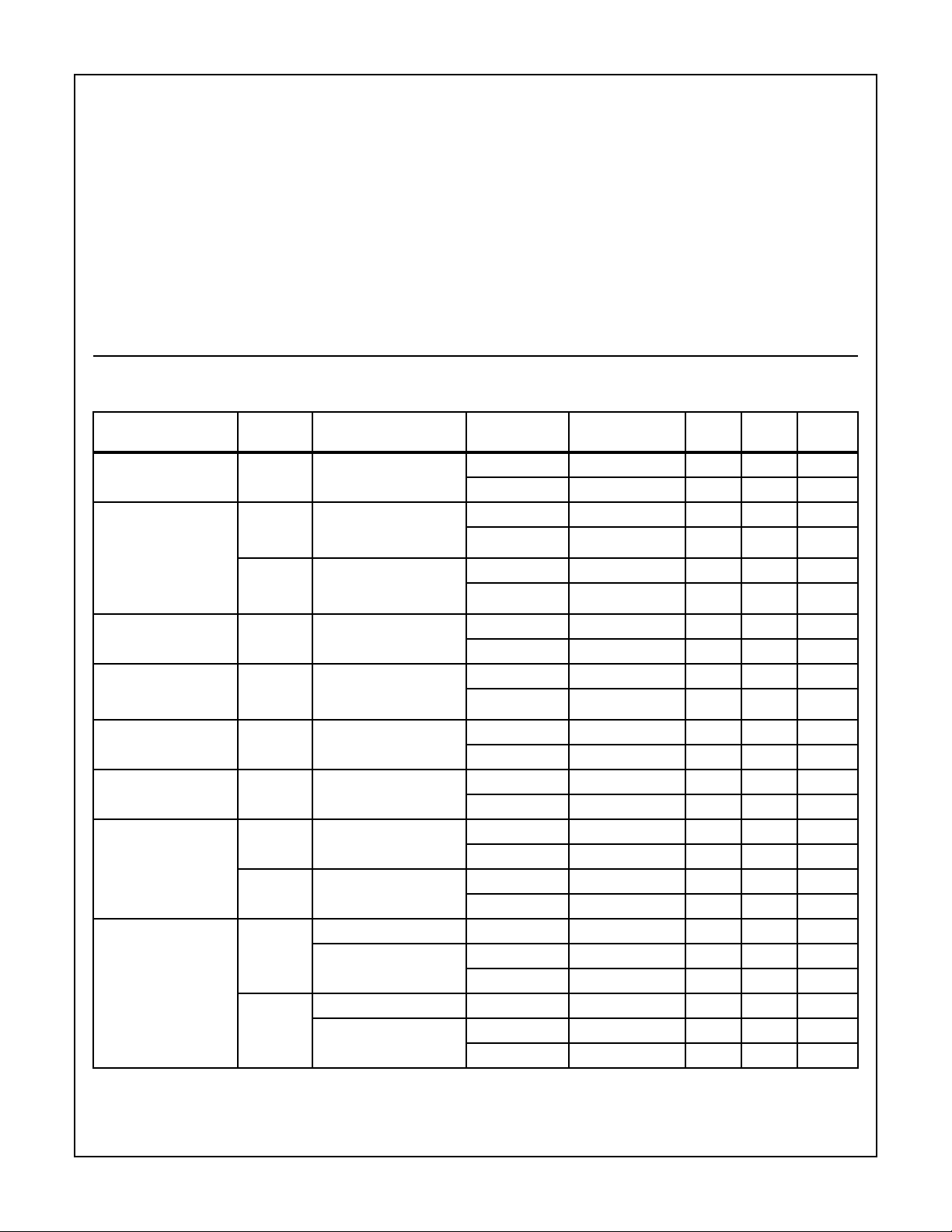
TABLE 1. DC ELECTRICAL PERFORMANCE SPECIFICATIONS
Device Tested at: V
PARAMETER SYMBOL CONDITIONS
Output Offset Voltage V
Power Supply
Rejection Ratio
Input Current I
Input Current Common
Mode Rejection
Input Resistance R
Gain (V
OUT
= 2V
P-P
Output Voltage Swing V
Output Voltage Swing V
= ±5V, R
SUPPLY
OS
PSRRP ∆V
PSRRN ∆V
BSP
CMS
IN
)A
VP1
OP100RL
V
ON100RL
OP50
V
ON50RL
SOURCE
= 0Ω, RL = 100Ω, V
VCM = 0V 1 25 -25 25 mV
= ±1.25V
SUP
V+ = 6.25V, V- = -5V
V+ = 3.75V, V- = -5V
= ±1.25V
SUP
V+ = 5V, V- = -6.25V
V+ = 5V, V- = -3.75V
VCM = 0V 1 25 -40 40 µA
∆VCM = ±2V
IBP
V+ = 3V, V- = -7V
V+ = 7V, V- = -3V
Note 2 1 25 25 - kΩ
VIN = -1V to +1V 1 25 0.980 1.020 V/V
= 100Ω, VIN = +3.3V 1 25 3 - V
= 100Ω, VIN = -3.3V 1 25 - -3 V
RL = 50Ω, VIN = +2.7V 1 25 2.5 - V
RL = 50Ω, VIN = +3.3V 2 125 2.5 - V
= 50Ω, VIN = -2.7V 1 25 - -2.5 V
RL = 50Ω, VIN = -3.3V 2 125 - -2.5 V
Thermal Resistance (Typical, Note 1) θJA(oC/W) θJC(oC/W)
CERDIP Package . . . . . . . . . . . . . . . . 120 35
Maximum Package Power Dissipation at 75oC
CERDIP Package . . . . . . . . . . . . . . . . . . . . . . . . . . . . . . . . 0.83W
Package Power Dissipation Derating Factor above 75oC
CERDIP Package . . . . . . . . . . . . . . . . . . . . . . . . . . . . .8.3mW/oC
Junction Temperature . . . . . . . . . . . . . . . . . . . . . . . . . . . . . . .175oC
Storage Temperature Range. . . . . . . . . . . . . . . -65oC ≤ TA≤ 150oC
Lead Temperature (Soldering 10s) . . . . . . . . . . . . . . . . . . . . 300oC
= 0V, Unless Otherwise Specified.
OUT
GROUP A
SUBGROUPS
TEMPERATURE
(oC) MIN MAX UNITS
2, 3 125, -55 -40 40 mV
12539-dB
2, 3 125, -55 35 - dB
12539-dB
2, 3 125, -55 35 - dB
2, 3 125, -55 -65 65 µA
125-40µA/V
2, 3 125, -55 - 50 µA/V
2, 3 125, -55 20 - kΩ
2, 3 125, -55 0.975 1.025 V/V
2, 3 125, -55 2.5 - V
2, 3 125, -55 - -2.5 V
3 -55 1.5 - V
3 -55 - -1.5 V
Spec Number 511083-883
2

HFA1110/883
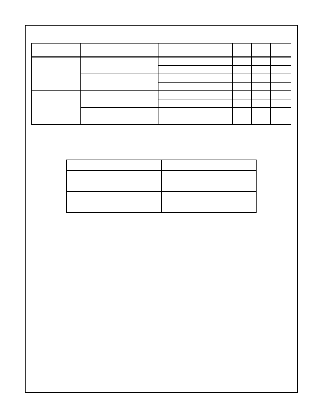
TABLE 1. DC ELECTRICAL PERFORMANCE SPECIFICATIONS (Continued)
Device Tested at: V
PARAMETER SYMBOL CONDITIONS
Output Current +I
Quiescent Power
Supply Current
NOTES:
2. Guaranteed from Input Common Mode Rejection Test, by: RIN = 1/CMS
3. Guaranteed from V
SUPPLY
= ±5V, R
SOURCE
= 0Ω, RL = 100Ω, V
= 0V, Unless Otherwise Specified.
OUT
SUBGROUPS
OUT
-I
OUT
I
CC
I
EE
Test with RL = 50Ω, by: I
OUT
Note 3 1, 2 25, 125 50 - mA
Note 3 1, 2 25, 125 - -50 mA
RL = 100Ω 1251426mA
RL = 100Ω 1 25 -26 -14 mA
= V
OUT
/50Ω.
OUT
TABLE 2. ELECTRICAL TEST REQUIREMENTS
MIL-STD-883 TEST REQUIREMENTS SUBGROUPS (SEE TABLE 1)
GROUP A
TEMPERATURE
(oC) MIN MAX UNITS
3 -55 30 - mA
3 -55 - -30 mA
2, 3 125, -55 - 33 mA
2, 3 125, -55 -33 - mA
.
IBP
Interim Electrical Parameters (Pre Burn-In) 1
Final Electrical Test Parameters 1 (Note 7), 2, 3
Group A Test Requirements 1, 2, 3
Groups C and D Endpoints 1
NOTE:
4. PDA applies to Subgroup 1 only.
Spec Number 511083-883
3

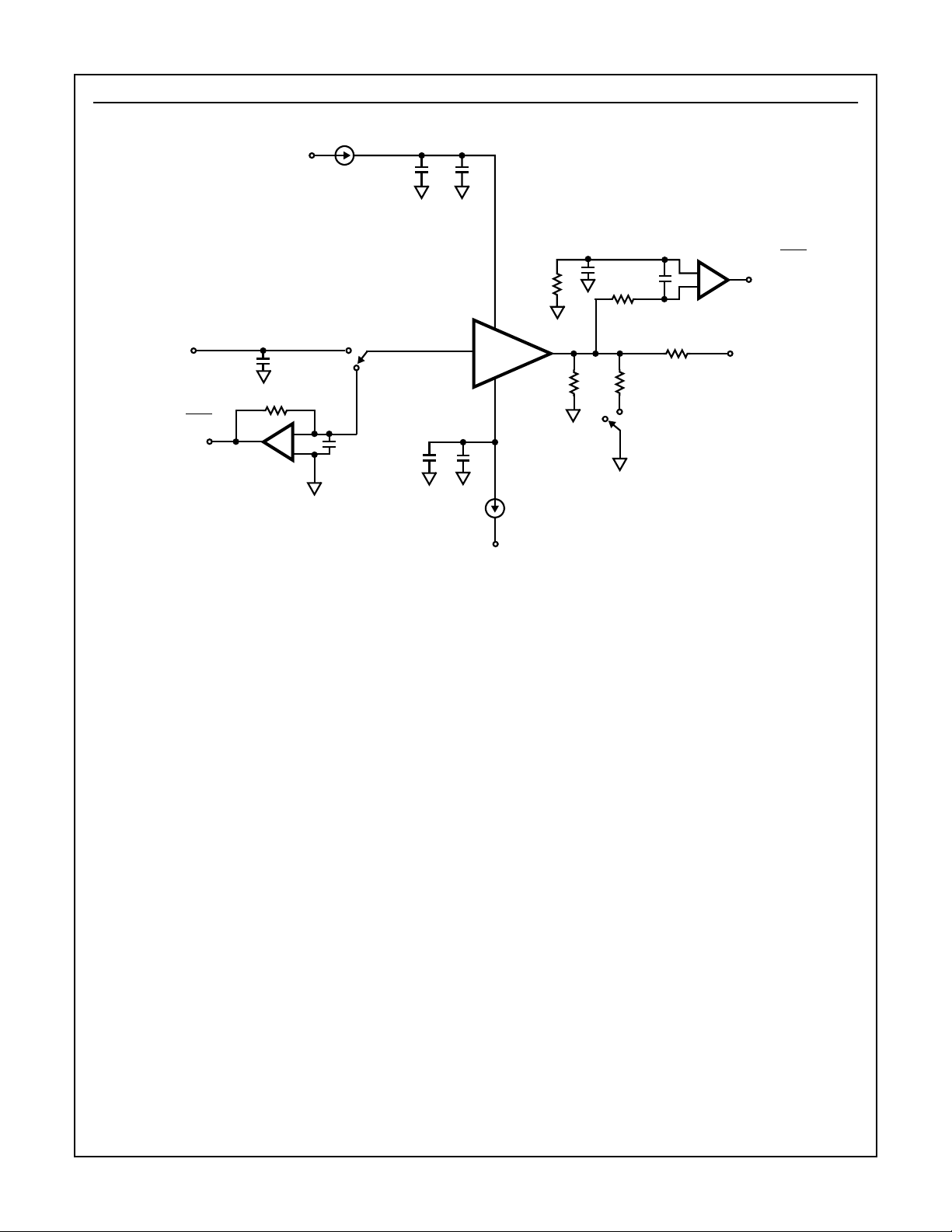
Test Circuit (Applies to Table 1)
HFA1110/883
I
BIAS
V+
I
CC
V
IN
V
Z
=
100K
V
Z
0.1
100K (0.01%)
HA-5177
-
+
1
K1
0.1
+
10 0.1
V
Y
VOS=
V
OUT
100
V
Y
0.1
510
1
I
EE
8
100 100
4
DUT
2
5
10 0.1
+
470pF
510
K3
NOTE:
1K
+
x100
All Resistors = ±1% (Ω)
All Capacitors = ±10% (µF)
V-
Unless Otherwise Noted
Chip Components Recommended
Spec Number 511083-883
4
 Loading...