March 1997
HFA1109
450MHz, Low Power, Current Feedback
Video Operational Amplifier
Features
• Wide - 3dB Bandwidth (AV = +2). . . . . . . . . . . . 450MHz
• Gain Flatness (To 250MHz) . . . . . . . . . . . . . . . . . . 0.8dB
• Very Fast Slew Rate (A
• High Input Impedance . . . . . . . . . . . . . . . . . . . . . 1.7MΩ
• Differential Gain/Phase . . . . . . . . . 0.02%/0.02 Degrees
• Low Supply Current . . . . . . . . . . . . . . . . . . . . . . . 10mA
= +2). . . . . . . . . . . . . 1100V/µs
V
Applications
• Professional Video Processing
• Video Switchers and Routers
• Medical Imaging
• PC Multimedia Systems
• Video Distribution Amplifiers
• Flash Converter Drivers
• Radar/IF Processing
Description
The HFA1109 is a high speed, low power, current feedback
amplifier built with Intersil’s proprietary complementary bipolar UHF-1 process. This amplifier features a unique combination of power and performance specifically tailored for
video applications.
The HFA1109 is a standard pinout op amp. It is a higher
performance, drop-in replacement (no feedback resistor
change required) for the CLC409.
If a comparably performing op amp with an output disable
function (useful for video multiplexing) is required, please
refer to the HFA1149 data sheet.
Ordering Information
PART NUMBER
(BRAND)
HFA1109IP -40 to 85 8 Ld PDIP E8.3
HFA1109IB (H1109) -40 to 85 8 Ld SOIC M8.15
HFA11XXEVAL DIP Evaluation Board for High Speed
TEMP.
RANGE (oC) PACKAGE
Op Amps
PKG.
NO.
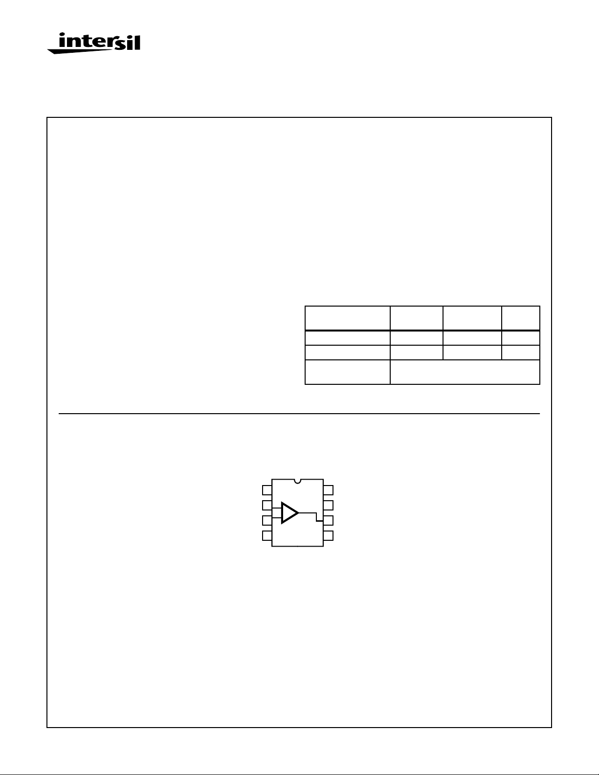
Pinout
NC
-IN
+IN
V-
HFA1109
(PDIP, SOIC)
TOP VIEW
1
2
+
3
4
8
NC
7
V+
6
OUT
5
NC
CAUTION: These devices are sensitive to electrostatic discharge; follow proper IC Handling Procedures.
1-888-INTERSIL or 321-724-7143 | Copyright © Intersil Corporation 1999
1
File Number 4019.3

HFA1109
Absolute Maximum Ratings Thermal Information
Voltage Between V+ and V- . . . . . . . . . . . . . . . . . . . . . . . . . . . . 12V
DC Input Voltage . . . . . . . . . . . . . . . . . . . . . . . . . . . . . . . . V
SUPPLY
Differential Input Voltage. . . . . . . . . . . . . . . . . . . . . . . . . . . . . . . . 8V
Output Current (Note 2) . . . . . . . . . . . . . . . . Short Circuit Protected
30mA Continuous
60mA ≤ 50% Duty Cycle
ESD Rating
Human Body Model (Per MIL-STD-883 Method 3015.7) . . 1400V
Charged Device Model (Per EOS/ESD DS5.3, 4/14/93). . . 2000V
Machine Model (Per EIAJ ED-4701Method C-111) . . . . . . . . 50V
Operating Conditions
Temperature Range . . . . . . . . . . . . . . . . . . . . . . . . . -40oC to 85oC
CAUTION: Stresses above those listed in “Absolute Maximum Ratings” may cause permanent damage to the device. This is a stress only rating and operation
of the device at these or any other conditions above those indicated in the operational sections of this specification is not implied.
NOTES:
1. θJA is measured with the component mounted on an evaluation PC board in free air.
2. Output is short circuit protected to ground. Brief short circuits to ground will not degrade reliability, however continuous (100% duty cycle)
output current must not exceed 30mA for maximum reliability.
Thermal Resistance (Typical, Note 1) θJA (oC/W)
PDIP Package. . . . . . . . . . . . . . . . . . . . . . . . . . . . . 130
SOIC Package. . . . . . . . . . . . . . . . . . . . . . . . . . . . . 170
Maximum Junction Temperature (Die). . . . . . . . . . . . . . . . . . . . 175oC
Maximum Junction Temperature (Plastic Package) . . . . . . . . 150oC
Maximum Storage Temperature Range . . . . . . . . . -65oC to 150oC
Maximum Lead Temperature (Soldering 10s) . . . . . . . . . . . . 300oC
(SOIC - Lead Tips Only)
Electrical Specifications V
= ±5V, AV= +2, RF= 250Ω, RL = 100Ω, Unless Otherwise Specified
SUPPLY
(NOTE 3)
PARAMETER TEST CONDITIONS
TEST
LEVEL
TEMP.
(oC) MIN TYP MAX UNITS
INPUT CHARACTERISTICS
Input Offset Voltage A 25 - 1 5 mV
A Full - 2 8 mV
Average Input Offset Voltage Drift B Full - 10 - µV/oC
Input Offset Voltage
Common-Mode Rejection Ratio
Input Offset Voltage
Power Supply Rejection Ratio
∆V
= ±2V A 25 47 50 - dB
CM
= ±2V A Full 45 48 - dB
∆V
CM
= ±1.25V A 25 50 53 - dB
∆V
PS
∆V
= ±1.25V A Full 47 51 - dB
PS
Non-Inverting Input Bias Current A 25 - 4 10 µA
A Full - 5 15 µA
Non-Inverting Input Bias Current Drift B Full - 30 - nA/
Non-Inverting Input Bias Current
Power Supply Sensitivity
= ±1.25V A 25 - 0.5 1 µA/V
∆V
PS
∆V
= ±1.25V A Full - 0.5 3 µA/V
PS
Inverting Input Bias Current A 25 - 2 10 µA
A Full - 3 15 µA
Inverting Input Bias Current Drift B Full - 40 - nA/
Inverting Input Bias Current
Common-Mode Sensitivity
Inverting Input Bias Current
Power Supply Sensitivity
Non-Inverting Input Resistance ∆V
= ±2V A 25 - 3 6 µA/V
∆V
CM
= ±2V A Full - 3 8 µA/V
∆V
CM
= ±1.25V A 25 - 1.6 5 µA/V
∆V
PS
= ±1.25V A Full - 1.6 8 µA/V
∆V
PS
= ±2V A 25, 85 0.8 1.7 - MΩ
CM
= ±2V A -40 0.5 1.4 - MΩ
∆V
CM
Inverting Input Resistance B 25 - 60 - Ω
Input Capacitance B 25 - 1.6 - pF
o
C
o
C
2

HFA1109
Electrical Specifications V
= ±5V, AV= +2, RF= 250Ω, RL = 100Ω, Unless Otherwise Specified (Continued)
SUPPLY
(NOTE 3)
PARAMETER TEST CONDITIONS
Input Voltage Common Mode Range
(Implied by VIO CMRR, +RIN, and -I
TEST
LEVEL
A Full ±2 ±2.5 - V
BIAS
TEMP.
(oC) MIN TYP MAX UNITS
CMS tests)
Input Noise Voltage Density (Note 4) f = 100kHz B 25 - 4 - nV/√
Non-Inverting Input Noise Current Density
f = 100kHz B 25 - 2.4 - pA/√
(Note 4)
Inverting Input Noise Current Density
f = 100kHz B 25 - 40 - pA/√
(Note 4)
TRANSFER CHARACTERISTICS
Open Loop Transimpedance Gain (Note 4) B 25 - 500 - kΩ
Minimum Stable Gain B Full - 1 - V/V
AC CHARACTERISTICS
-3dB Bandwidth
= 0.2V
(V
OUT
P-P
, Note 4)
AV = -1, RF = 200Ω B 25 300 375 - MHz
B Full 290 360 - MHz
= +1, +RS = 550Ω(PDIP),
A
V
+RS = 700Ω (SOIC)
B 25 280 330 - MHz
B Full 260 320 - MHz
AV = +2 B 25 390 450 - MHz
B Full 350 410 - MHz
Gain Peaking A
= +2, V
V
OUT
= 0.2V
P-P
B 25 - 0 0.2 dB
B Full - 0 0.5 dB
Gain Flatness
= +2, V
(A
V
OUT
= 0.2V
P-P
, Note 4)
To 125MHz B 25 -1.0 -0.45 - dB
B Full -1.1 -0.45 - dB
To 200MHz B 25 -1.6 -0.75 - dB
B Full -1.7 -0.75 - dB
To 250MHz B 25 -1.9 -0.85 - dB
B Full -2.2 -0.85 - dB
Gain Flatness
= +1, +RS = 550Ω (PDIP),
(A
V
+RS = 700Ω (SOIC), V
Note 4)
OUT
= 0.2V
P-P
,
To 125MHz B 25 ±0.3 ±0.1 - dB
B Full ±0.4 ±0.1 - dB
To 200MHz B 25 ±0.8 ±0.35 - dB
B Full ±0.9 ±0.35 - dB
To 250MHz B 25 ±1.3 ±0.6 - dB
B Full ±1.4 ±0.6 - dB
OUTPUT CHARACTERISTICS
Output Voltage Swing, Unloaded
(Note 4)
Output Current
(Note 4)
Output Short Circuit Current A
Closed Loop Output Resistance (Note 4) DC, A
Second Harmonic Distortion
(V
OUT
= 2V
P-P
, Note 4)
= -1, RL = ∞ A25±3 ±3.2 - V
A
V
A Full ±2.8 ±3- V
AV = -1, RL = 75Ω A 25, 85 ±33 ±36 - mA
A -40 ±30 ±33 - mA
= -1 B 25 - 120 - mA
V
= +1 B 25 - 0.05 - Ω
V
20MHz B 25 - -55 - dBc
60MHz B 25 - -57 - dBc
Hz
Hz
Hz
3

HFA1109
Electrical Specifications V
= ±5V, AV= +2, RF= 250Ω, RL = 100Ω, Unless Otherwise Specified (Continued)
SUPPLY
(NOTE 3)
PARAMETER TEST CONDITIONS
Third Harmonic Distortion
(V
OUT
= 2V
P-P
, Note 4)
TEST
LEVEL
20MHz B 25 - -68 - dBc
60MHz B 25 - -60 - dBc
TEMP.
(oC) MIN TYP MAX UNITS
Reverse Isolation (S12) 30MHz B 25 - -65 - dB
TRANSIENT CHARACTERISTICS
Rise and Fall Times V
OUT
= 0.5V
P-P
B 25 - 1.1 1.3 ns
B Full - 1.1 1.4 ns
Overshoot V
OUT
= 0.5V
P-P
B25-02%
B Full - 0.5 5 %
Slew Rate AV = -1, RF= 200Ω
V
= 5V
A
OUT
V
= +1, V
P-P
OUT
= 4V
+RS = 550Ω (PDIP),
+RS = 700Ω (SOIC)
A
= +2, V
V
OUT
= 5V
P-P
P-P
,
B 25 2300 2600 - V/µs
B Full 2200 2500 - V/µs
B 25 475 550 - V/µs
B Full 430 500 - V/µs
B 25 940 1100 - V/µs
B Full 800 950 - V/µs
Settling Time
= +2V to 0V step, Note 4)
(V
OUT
To 0.1% B 25 - 19 - ns
To 0.05% B 25 - 23 - ns
To 0.01% B 25 - 36 - ns
Overdrive Recovery Time V
= ±2V B 25 - 5 - ns
IN
VIDEO CHARACTERISTICS
Differential Gain
(f = 3.58MHz)
= 150Ω B 25 - 0.02 0.06 %
R
L
B Full - 0.03 0.09 %
= 75Ω B 25 - 0.04 0.09 %
R
L
B Full - 0.05 0.12 %
Differential Phase
(f = 3.58MHz)
RL = 150Ω B 25 - 0.02 0.06 Degrees
B Full - 0.02 0.06 Degrees
RL = 75Ω B 25 - 0.05 0.09 Degrees
B Full - 0.06 0.13 Degrees
POWER SUPPLY CHARACTERISTICS
Power Supply Range C 25 ±4.5 - ±5.5 V
Power Supply Current (Note 4) A 25 - 9.6 10 mA
A Full - 10 11 mA
NOTES:
3. Test Level: A. Production Tested; B. Typical or Guaranteed Limit Based on Characterization; C. Design Typical for Information Only.
4. See Typical Performance Curves for more information.
4
 Loading...