Intersil Corporation HFA1100-883 Datasheet

HFA1100/883
July 1994
Features
• This Circuit is Processed in Accordance to MIL-STD883 and is Fully Conformant Under the Provisions of
Paragraph 1.2.1.
• Low Distortion (HD3, 30MHz) . . . . . . . . . . -84dBc (Typ)
• Wide -3dB Bandwidth . . . . . . . . . . . . . . . 850MHz (Typ)
• Very High Slew Rate . . . . . . . . . . . . . . . 2300V/µs (Typ)
• Fast Settling (0.1%) . . . . . . . . . . . . . . . . . . . . 11ns (Typ)
• Excellent Gain Flatness (to 50MHz) . . . . . 0.05dB (Typ)
• High Output Current . . . . . . . . . . . . . . . . . . 65mA (Typ)
• Fast Overdrive Recovery. . . . . . . . . . . . . . . <10ns (Typ)
Applications
• Video Switching and Routing
• Pulse and Video Amplifiers
• Wideband Amplifiers
• RF/IF Signal Processing
850MHz Current Feedback Amplifier
Description
The HFA1100/883 is a high speed, wideband, fast settling
current feedback amplifier. Built with Intersil’ proprietary,
complementary bipolar UHF-1 process, it is the fastest
monolithic amplifier available from any semiconductor manufacturer.
The HFA1100/883’s wide bandwidth, fast settling characteristic, and low output impedance, make this amplifier ideal for
driving fast A/D converters.
Component and composite video systems will also benefit
from this amplifier’s performance, as indicated by the excellent gain flatness, and 0.03%/0.05 Deg. Differential Gain/
Phase specifications (R
Ordering Information
PART NUMBER
HFA1100MJ/883 -55oC to +125oC 8 Lead CerDIP
=75Ω).
L
TEMPERATURE
RANGE PACKAGE
• Flash A/D Driver
• Medical Imaging Systems
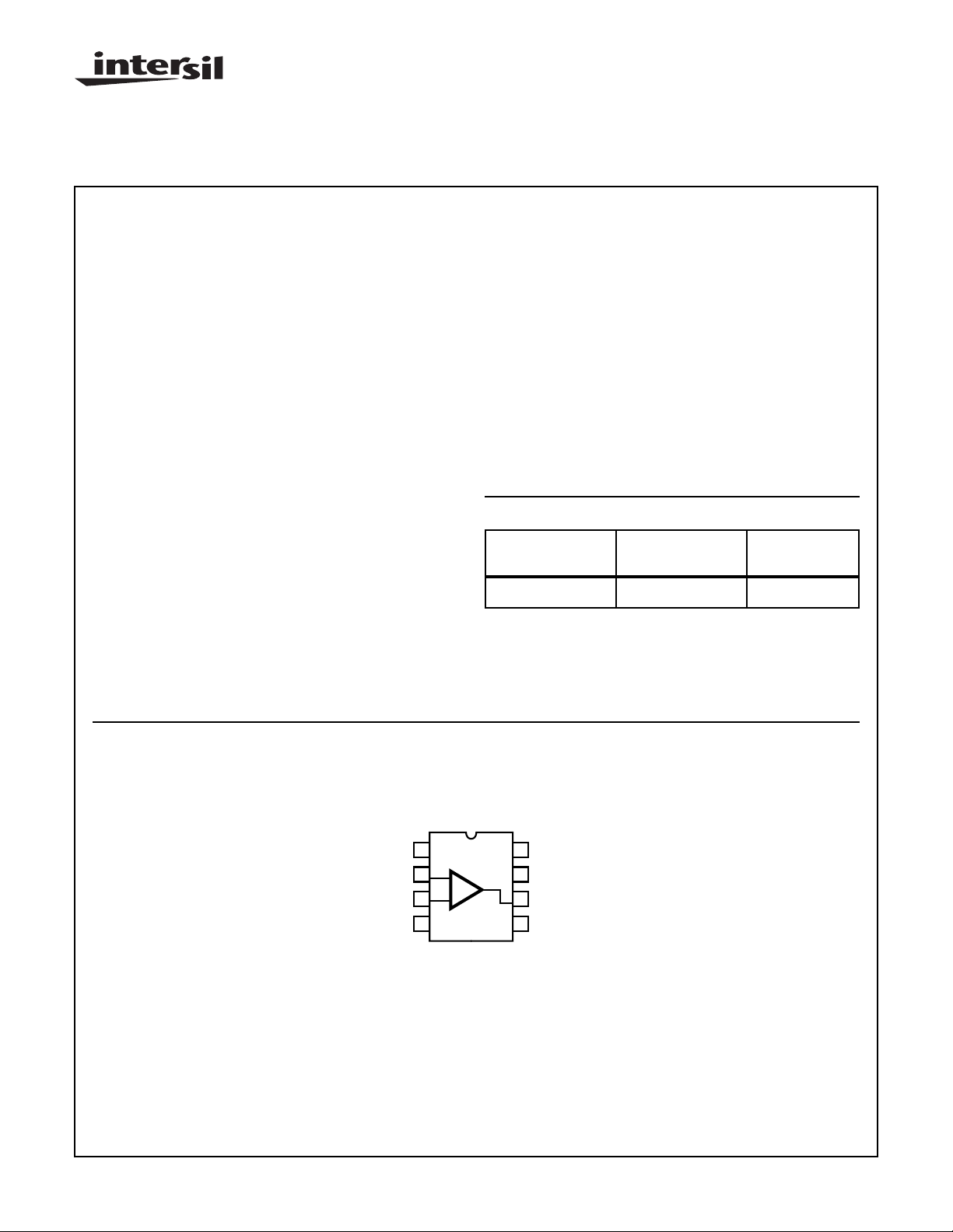
Pinout
NC
-IN
+IN
1
2
3
4
V-
HFA1100/883
(CERDIP)
TOP VIEW
-
+
8
NC
7
V+
6
OUT
5
NC
CAUTION: These devices are sensitive to electrostatic discharge; follow proper IC Handling Procedures.
http://www.intersil.com or 407-727-9207
| Copyright © Intersil Corporation 1999
3-174
Spec Number 511104-883
File Number 3615.1

Specifications HFA1100/883
Absolute Maximum Ratings Thermal Information
Voltage Between V+ and V- . . . . . . . . . . . . . . . . . . . . . . . . . . . . 12V
Differential Input Voltage . . . . . . . . . . . . . . . . . . . . . . . . . . . . . . . 5V
Voltage at Either Input Terminal . . . . . . . . . . . . . . . . . . . . . . V+ to V-
Output Current (50% Duty Cycle) . . . . . . . . . . . . . . . . . . . . . . . .±55mA
Junction Temperature. . . . . . . . . . . . . . . . . . . . . . . . . . . . . . +175oC
ESD Rating. . . . . . . . . . . . . . . . . . . . . . . . . . . . . . . . . . . . . .< 2000V
Storage Temperature Range . . . . . . . . . . . . . . -65oC ≤ TA≤ +150oC
Lead Temperature (Soldering 10s). . . . . . . . . . . . . . . . . . . . +300oC
CAUTION: Stresses above those listed in “Absolute Maximum Ratings” may cause permanent damage to the device. This is a stress only rating and operation
of the device at these or any other conditions above those indicated in the operational sections of this specification is not implied.
Operating Conditions
Operating V
Operating Temperature Range. . . . . . . . . . . . .-55oC ≤ TA≤ +125oC
Device Tested at: V
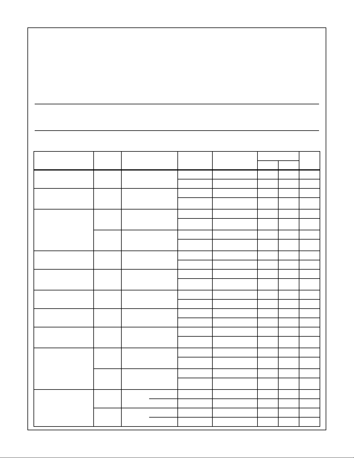
PARAMETERS SYMBOL CONDITIONS
Input Offset Voltage V
Common Mode
Rejection Ratio
Power Supply
Rejection Ratio
Non-Inverting Input (+IN)
Current
+IN Current Common
Mode Sensitivity
+IN Resistance +R
Inverting Input (-IN)
Current
-IN Current Common
Mode Sensitivity
-IN Current Power
Supply Sensitivity
Output Voltage Swing V
(±VS) . . . . . . . . . . . . . . . . . . . . . . . . . . . . . . . . . ±5V
SUPPLY
TABLE 1. DC ELECTRICAL PERFORMANCE CHARACTERISTICS
= ±5V, AV= +1, RF= 510Ω, R
SUPPLY
VCM= 0V 1 +25oC-66mV
IO
CMRR ∆VCM= ±2V
V+ = 3V, V- = -7V
V+ = 7V, V- = -3V
PSRRP ∆V
SUPPLY
V+ = 6.25V, V- = -5V
V+ = 3.75V, V- = -5V
PSRRN ∆V
SUPPLY
V+ = 5V, V- = -6.25V
V+ = 5V, V- = -3.75V
I
BSP
CMS
VCM= 0V 1 +25oC -40 40 µA
∆VCM= ±2V
IBP
V+ = 3V, V- = -7V
V+ = 7V, V- = -3V
Note 1 1 +25oC25-kΩ
IN
I
BSN
CMS
VCM= 0V 1 +25oC -50 50 µA
∆VCM= ±2V
IBN
V+ = 3V, V- = -7V
V+ = 7V, V- = -3V
PPSS
IBN
∆V
SUPPLY
V+ = 6.25V, V- = -5V
V+ = 3.75V, V- = -5V
NPSS
IBN
∆V
SUPPLY
V+ = 5V, V- = -6.25V
V+ = 5V, V- = -3.75V
OP100
AV=-1
RL= 100Ω
V
ON100
AV=-1
RL= 100Ω
SOURCE
= ±1.25V
= ±1.25V
= ±1.25V
= ±1.25V
VIN= -3.5V 1 +25oC3-V
VIN= -3V 2, 3 +125oC, -55oC 2.5 - V
VIN=+3.5V 1 +25oC - -3 V
VIN= +3V 2, 3 +125oC, -55oC - -2.5 V
Thermal Resistance θ
CerDIP Package . . . . . . . . . . . . . . . . . 115oC/W 30oC/W
Maximum Package Power Dissipation at +75oC
CerDIP Package . . . . . . . . . . . . . . . . . . . . . . . . . . . . . . . . .0.87W
Package Power Dissipation Derating Factor above +75oC
CerDIP Package . . . . . . . . . . . . . . . . . . . . . . . . . . . . . .8.7mW/oC
RL≥ 50Ω
= 0Ω, RL = 100Ω, V
= 0V, Unless Otherwise Specified.
OUT
GROUP A
SUBGROUPS TEMPERATURE
2, 3 +125oC, -55oC -10 10 mV
1 +25oC40-dB
2, 3 +125oC, -55oC38 - dB
1 +25oC45-dB
2, 3 +125oC, -55oC42 - dB
1 +25oC45-dB
2, 3 +125oC, -55oC42 - dB
2, 3 +125oC, -55oC -65 65 µA
1 +25oC-40µA/V
2, 3 +125oC, -55oC-50µA/V
2, 3 +125oC, -55oC20 - kΩ
2, 3 +125oC, -55oC -75 75 µA
1 +25oC-7µA/V
2, 3 +125oC, -55oC-10µA/V
1 +25oC-15µA/V
2, 3 +125oC, -55oC-27µA/V
1 +25oC-15µA/V
2, 3 +125oC, -55oC-27µA/V
JA
LIMITS
θ
JC
UNITSMIN MAX
3-175
Spec Number 511104-883

Specifications HFA1100/883
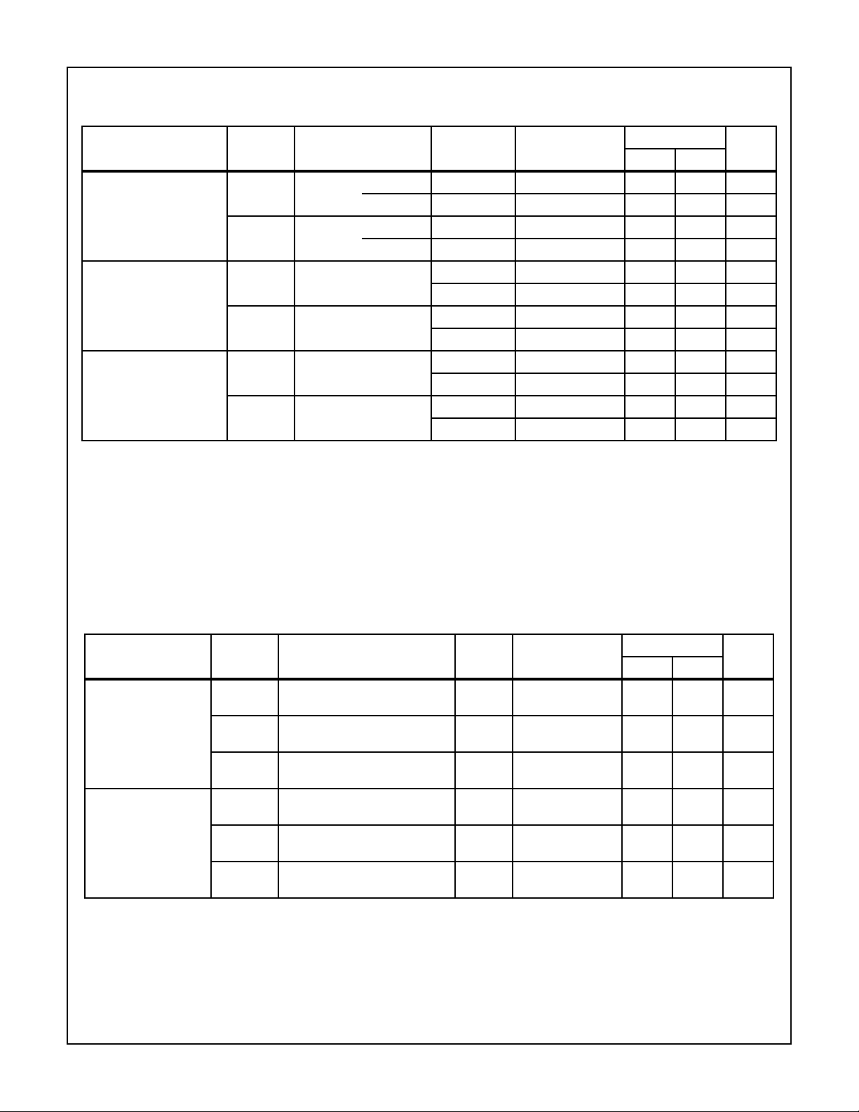
TABLE 1. DC ELECTRICAL PERFORMANCE CHARACTERISTICS (Continued)
Device Tested at: V
PARAMETERS SYMBOL CONDITIONS
Output Voltage Swing V
Output Current +I
Quiescent Power
Supply Current
NOTES:
1. Guaranteed from +IN Common Mode Rejection Test, by: +RIN= 1/CMS
2. Guaranteed from V
= ±5V, AV= +1, RF= 510Ω, R
SUPPLY
OP50
V
ON50
OUT
-I
OUT
I
CC
I
EE
Test with RL=50Ω, by: I
OUT
= 0Ω, RL = 100Ω, V
SOURCE
AV=-1
RL=50Ω
AV=-1
RL=50Ω
VIN= -3V 1, 2 +25oC, +125oC 2.5 - V
VIN= -2V 3 -55oC 1.5 - V
VIN= +3V 1, 2 +25oC, +125oC - -2.5 V
VIN= +2V 3 -55oC - -1.5 V
Note 2 1, 2 +25oC, +125oC50 - mA
Note 2 1, 2 +25oC, +125oC - -50 mA
RL= 100Ω 1 +25oC1426mA
RL= 100Ω 1 +25oC -26 -14 mA
OUT=VOUT
/50Ω.
= 0V, Unless Otherwise Specified.
OUT
GROUP A
SUBGROUPS TEMPERATURE
LIMITS
UNITSMIN MAX
3 -55oC30-mA
3 -55oC - -30 mA
2, 3 +125oC, -55oC - 33 mA
2, 3 +125oC, -55oC -33 - mA
.
IBP
TABLE 2. AC ELECTRICAL PERFORMANCE CHARACTERISTICS
Table 2 Intentionally Left Blank. See AC Specifications in Table 3
TABLE 3. ELECTRICAL PERFORMANCE CHARACTERISTICS
Device Characterized at: V
= ±5V, AV= +2, RF= 360Ω, RL = 100Ω, Unless Otherwise Specified.
SUPPLY
PARAMETERS SYMBOL CONDITIONS NOTES TEMPERATURE
-3dB Bandwidth BW(-1) AV= -1, RF= 430Ω
V
= 200mV
OUT
P-P
BW(+1) AV= +1, RF= 510Ω
V
= 200mV
OUT
P-P
BW(+2) AV= +2,
V
= 200mV
OUT
P-P
Gain Flatness GF30 AV= +2, RF= 510Ω, f ≤ 30MHz
V
= 200mV
OUT
P-P
GF50 AV= +2, RF= 510Ω, f ≤ 50MHz
V
= 200mV
OUT
P-P
GF100 AV= +2, RF= 510Ω, f ≤ 100MHz
V
= 200mV
OUT
P-P
1 +25oC 300 - MHz
1 +25oC 550 - MHz
1 +25oC 350 - MHz
1 +25oC-±0.04 dB
1 +25oC-±0.10 dB
1 +25oC-±0.30 dB
LIMITS
UNITSMIN MAX
3-176
Spec Number 511104-883

Specifications HFA1100/883
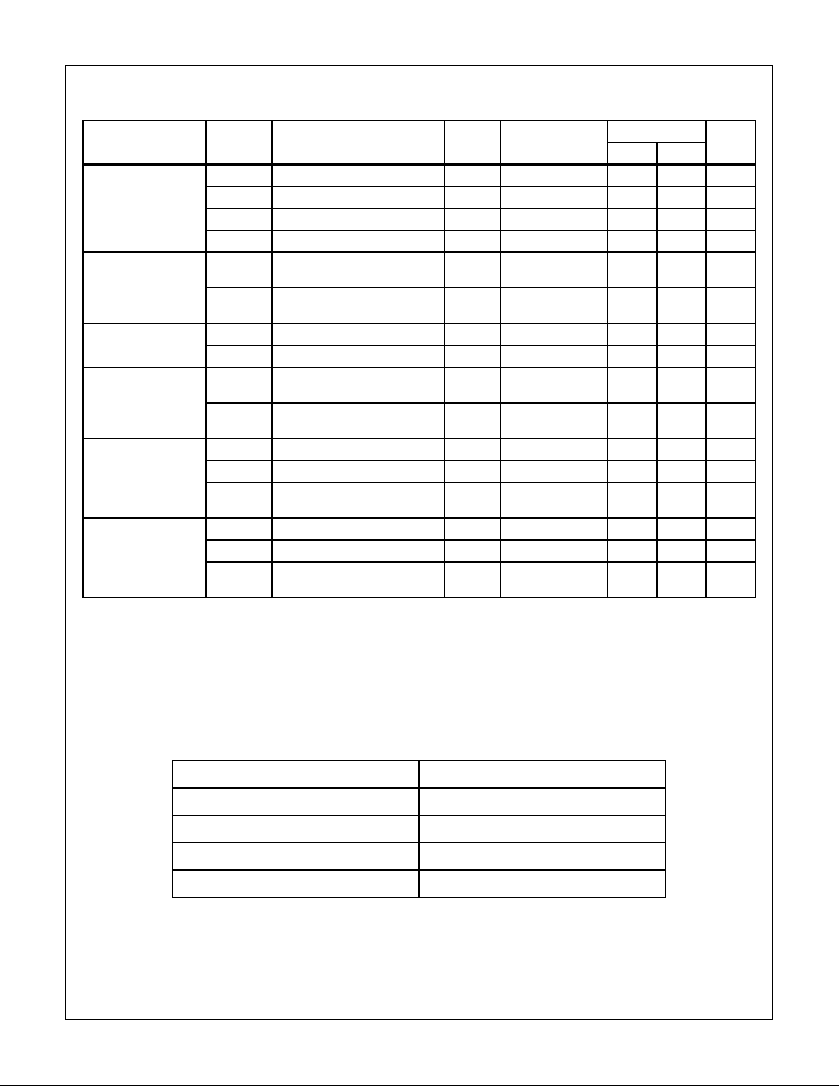
TABLE 3. ELECTRICAL PERFORMANCE CHARACTERISTICS (Continued)
Device Characterized at: V
PARAMETERS SYMBOL CONDITIONS NOTES TEMPERATURE
Slew Rate +SR(+1) AV= +1, RF= 510Ω,V
Rise and Fall Time T
= ±5V, AV= +2, RF= 360Ω, RL = 100Ω, Unless Otherwise Specified.
SUPPLY
-SR(+1) AV= +1, RF= 510Ω,V
+SR(+2) AV= +2, V
-SR(+2) AV= +2, V
AV= +2, V
R
OUT
OUT
OUT
= 5V
= 5V
= 0.5V
P-P
P-P
OUT
OUT
P-P
= 5V
= 5V
1, 2 +25oC 1200 - V/µs
P-P
1, 2 +25oC 1100 - V/µs
P-P
1, 2 +25oC 1650 - V/µs
1, 2 +25oC 1500 - V/µs
1, 2 +25oC-1ns
LIMITS
UNITSMIN MAX
T
Overshoot +OS AV= +2, V
-OS AV= +2, V
Settling Time TS(0.1) AV= +2, RF= 510Ω
TS(0.05) AV= +2, RF= 510Ω
2nd Harmonic
Distortion
HD2(30) AV= +2, f = 30MHz, V
HD2(50) AV= +2, f = 50MHz, V
HD2(100) AV= +2, f = 100MHz,
3rd Harmonic
Distortion
HD3(30) AV= +2, f = 30MHz,V
HD3(50) AV= +2, f = 50MHz, V
HD3(100) AV= +2, f = 100MHz,
F
AV= +2, V
V
OUT
V
OUT
V
OUT
V
OUT
OUT
OUT
OUT
= 2V to 0V, to 0.1%
= 2V to 0V, to 0.05%
= 2V
P- P
= 2V
P-P
= 0.5V
= 0.5V
= 0.5V
P-P
P-P
P-P
OUT
OUT
OUT
OUT
= 2V
= 2V
= 2V
= 2V
1, 2 +25oC-1ns
1, 3 +25oC - 25 %
1, 3 +25oC - 20 %
1 +25oC - 20 ns
1 +25oC - 33 ns
P-P
P-P
1 +25oC - -48 dBc
1 +25oC - -45 dBc
1 +25oC - -35 dBc
P-P
P-P
1 +25oC - -65 dBc
1 +25oC - -60 dBc
1 +25oC - -40 dBc
NOTES:
1. Parameters listed in Table 3 are controlled via design or process parameters and are not directly tested at final production. These parameters are lab characterized upon initial design release, or upon design changes. These parameters are guaranteed by characterization
based upon data from multiple production runs which reflect lot-to-lot and within lot variation.
2. Measured between 10% and 90% points.
3. For 200ps input transition times. Overshoot decreases as input transition times increase, especially for AV= +1. Please refer to
Performance Curves.
TABLE 4. ELECTRICAL TEST REQUIREMENTS
MIL-STD-883 TEST REQUIREMENTS SUBGROUPS (SEE TABLE 1)
Interim Electrical Parameters (Pre Burn-In) 1
Final Electrical Test Parameters 1 (Note 1), 2, 3
Group A Test Requirements 1, 2, 3
Groups C and D Endpoints 1
NOTE:
1. PDA applies to Subgroup 1 only.
3-177
Spec Number 511104-883

HFA1100/883
Die Characteristics
DIE DIMENSIONS:
63 x 44 x 19 mils ± 1 mils
1600µm x 1130µm x 483µm ± 25.4µm
METALLIZATION:
Type: Metal 1: AICu(2%)/TiW Type: Metal 2: AICu(2%)
Thickness: Metal 1: 8k
Å ± 0.4kÅ Thickness: Metal 2: 16kÅ ± 0.8kÅ
GLASSIVATION:
Type: Nitride
Thickness: 4k
WORST CASE CURRENT DENSITY:
2.0 x 10
Å ± 0.5kÅ
5
A/cm2at 47.5mA
TRANSISTOR COUNT: 52
SUBSTRATE POTENTIAL (Powered Up): Floating (Recommend Connection to V-)
Metallization Mask Layout
HFA1100/883
+IN
V
BAL
-IN
V-
L
OUT
BAL
V
H
V+
3-178
Spec Number 511104-883
 Loading...