Intersil Corporation HD-6402 Datasheet

March 1997
HD-6402
CMOS Universal Asynchronous
Receiver Transmitter (UART)
Features
• 8.0MHz Operating Frequency (HD-6402B)
• 2.0MHz Operating Frequency (HD-6402R)
• Low Power CMOS Design
• Programmable Word Length, Stop Bits and Parity
• Automatic Data Formatting and Status Generation
• Compatible with Industry Standard UARTs
• Single +5V Power Supply
• CMOS/TTL Compatible Inputs
Description
The HD-6402 is a CMOS UART for interfacing computers or
microprocessors to an asynchronous serial data channel.
The receiver converts serial start, data, parity and stop bits.
The transmitter converts parallel data into serial form and
automatically adds start, parity and stop bits. The data word
length can be 5, 6, 7 or 8 bits. Parity may be odd or even.
Parity checking and generation can be inhibited. The stop
bits may be one or two or one and one-half when transmitting 5-bit code.
The HD-6402 can be used in a wide range of applications
including modems, printers, peripherals and remote data
acquisition systems. Utilizing the Intersil advanced scaled
SAJI IV CMOS process permits operation clock frequencies
up to 8.0MHz (500K Baud). Power requirements , by comparison, are reduced from 300mW to 10mW. Status logic
increases flexibility and simplifies the user interface.
Ordering Information
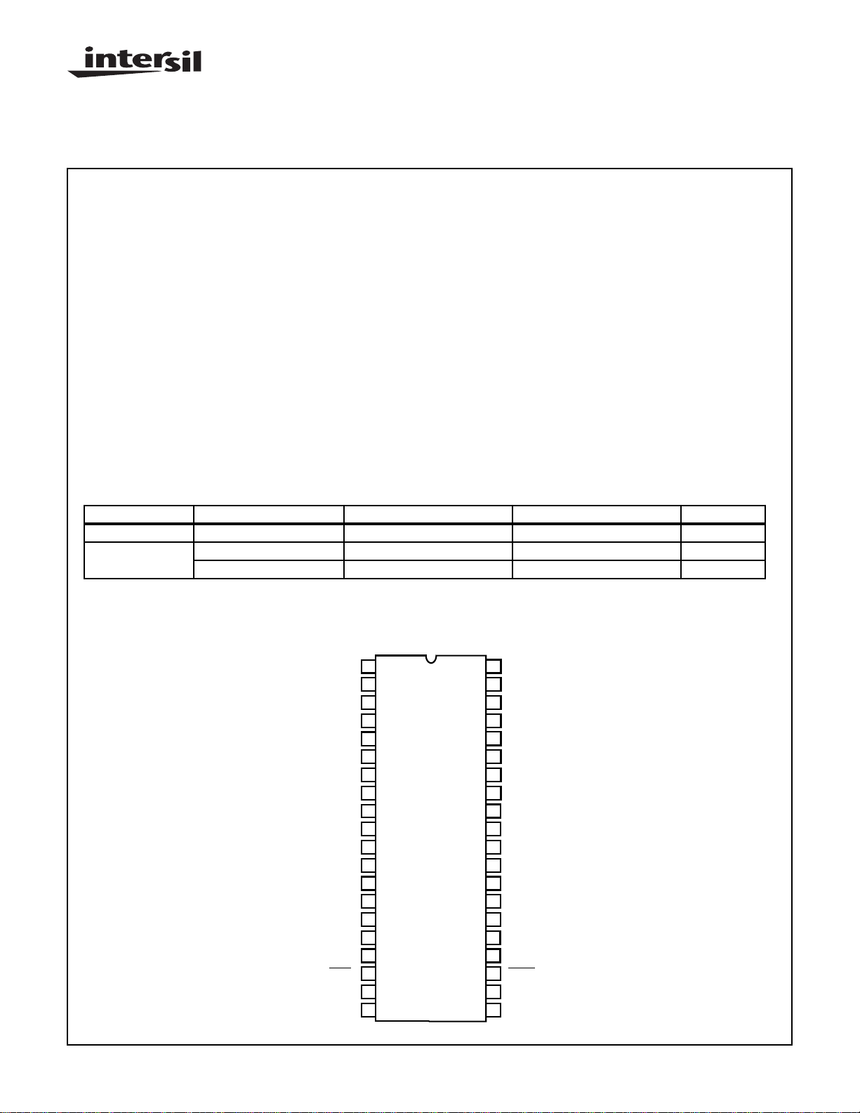
PACKAGE TEMPERATURE RANGE 2MHz = 125K BAUD 8MHz = 500K BAUD PKG. NO.
Plastic DIP -40oC to +85oC HD3-6402R-9 HD3-6402B-9 E40.6
CERDIP -40oC to +85oC HD1-6402R-9 HD1-6402B-9 F40.6
SMD# -55oC to +125oC 5962-9052501MQA 5962-9052502MQA F40.6
Pinout
HD-6402 (PDIP, CERDIP)
TOP VIEW
1
V
CC
2
NC
3
GND
4
RRD
5
RBR8
6
RBR7
7
RBR6
8
RBR5
RBR4
9
10
RBR3
11
RBR2
12
RBR1
13
PE
FE
14
15
OE
16
SFD
17
RRC
18
DRR
19
DR
RRI
20
CAUTION: These devices are sensitive to electrostatic discharge; follow proper IC Handling Procedures.
http://www.intersil.com or 407-727-9207
| Copyright © Intersil Corporation 1999
5-1
40
39
38
37
36
35
34
33
32
31
30
29
28
27
26
25
24
23
22
21
TRC
EPE
CLS1
CLS2
SBS
PI
CRL
TBR8
TBR7
TBR6
TBR5
TBR4
TBR3
TBR2
TBR1
TRO
TRE
TBRL
TBRE
MR
File Number 2956.1

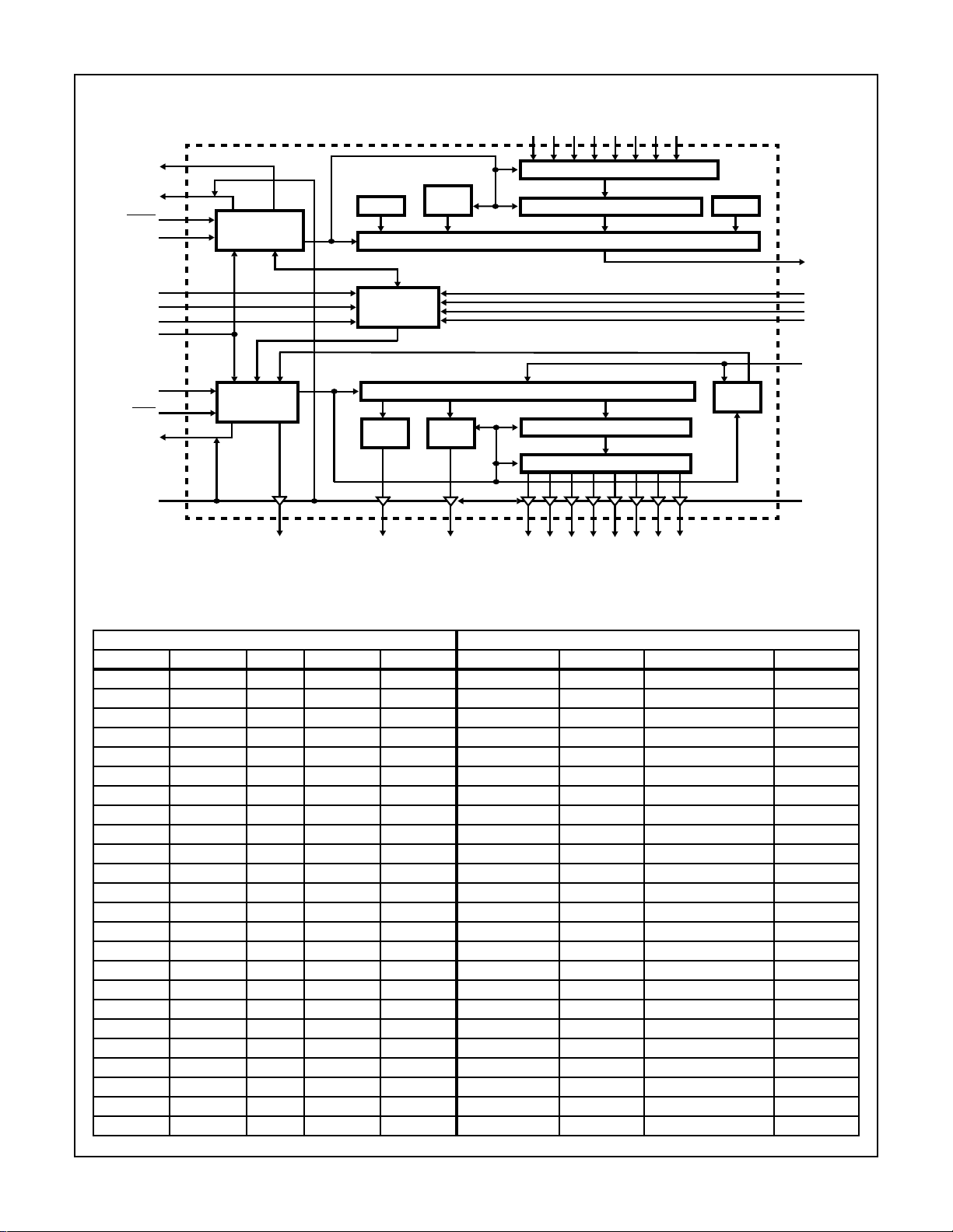
Functional Diagram
HD-6402
(28)
(26)
TBR1(27)
(30)
(32)
(33)TBR8
(31)
(29)
(24) TRE
(22) TBRE †
(23)
TBRL
(40) TRC
(38) CLS1
(37) CLS2
(34) CRL
(21) MR
(17) RRC
(18)
DRR
(19) DR †
(16) SFD
† THESE OUTPUTS ARE
THREE-STATE
TRANSMITTER
TIMING AND
CONTROL
RECEIVER
TIMING AND
CONTROL
† OE † FE † PE
(15)
STOP
CONTROL
REGISTER
STOP
LOGIC
(14)
PARITY
LOGIC
PARITY
LOGIC
(13)
3-STATE
BUFFERS
TRANSMITTER BUFFER REGISTER
TRANSMITTER REGISTER
MULTIPLEXER
MULTIPLEXER
RECEIVER REGISTER
RECEIVER BUFFER REGISTER
† RBR8
(5) (6) (7)
(8) (9) (10)(11) (12)
† RBR1
START
START
LOGIC
Control Definition
CONTROL WORD CHARACTER FORMAT
CLS 2 CLS 1 PI EPE SBS START BIT DATA BITS PARITY BIT STOP BITS
0 0 0 0 0 1 5 ODD 1
0 0 0 0 1 1 5 ODD 1.5
0 0 0 1 0 1 5 EVEN 1
0 0 0 1 1 1 5 EVEN 1.5
0 0 1 X 0 1 5 NONE 1
0 0 1 X 1 1 5 NONE 1.5
0 1 0 0 0 1 6 ODD 1
0 1 0 0 1 1 6 ODD 2
0 1 0 1 0 1 6 EVEN 1
0 1 0 1 1 1 6 EVEN 2
0 1 1 X 0 1 6 NONE 1
0 1 1 x 1 1 6 NONE 2
1 0 0 0 0 1 7 ODD 1
1 0 0 0 1 1 7 ODD 2
1 0 0 1 0 1 7 EVEN 1
1 0 0 1 1 1 7 EVEN 2
1 0 1 X 0 1 7 NONE 1
1 0 1 x 1 1 7 NONE 2
1 1 0 0 0 1 8 ODD 1
1 1 0 0 1 1 8 ODD 2
1 1 0 1 0 1 8 EVEN 1
1 1 0 1 1 1 8 EVEN 2
1 1 1 X 0 1 8 NONE 1
1 1 1 x 1 1 8 NONE 2
(25) TRO
(36) SBS
(16) SFD
(39) EPE
(35) PI
(20) RRI
(4) RRD
5-2

HD-6402
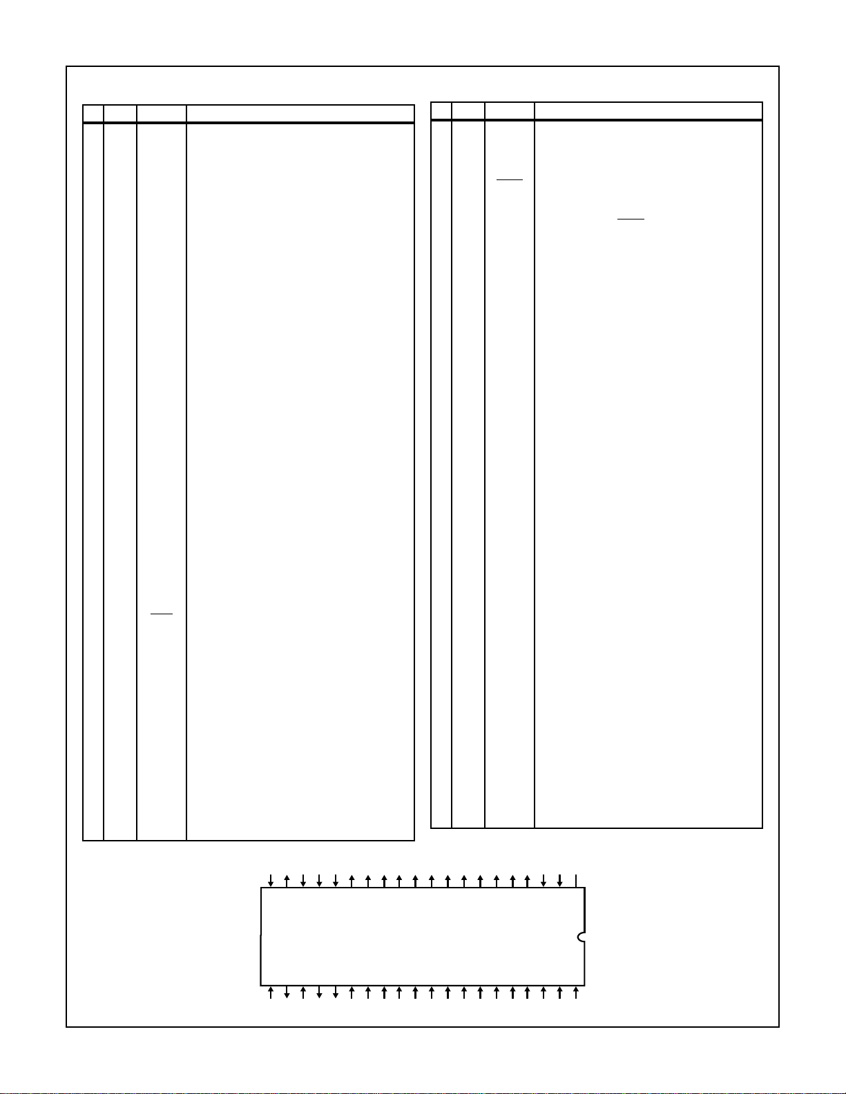
Pin Description
PIN TYPE SYMBOL DESCRIPTION
1V
2 NC No Connection
3 GND Ground
4 I RRD A high level on RECEIVER REGISTER DISABLE
5 O RBR8 The contents of the RECEIVER BUFFER REGIS-
6 O RBR7 See Pin 5-RBR8
7 O RBR6 See Pin 5-RBR8
8 O RBR5 See Pin 5-RBR8
9 O RBR4 See Pin 5-RBR8
10 O RBR3 See Pin 5-RBR8
11 O RBR2 See Pin 5-RBR8
12 O RBR1 See Pin 5-RBR8
13 O PE A high level on PARITY ERROR indicates receiv ed
14 O FE A high level on FRAMING ERROR indicates the
15 O OE A high level on OVERRUN ERROR indicates the
16 I SFD A high level on STATUS FLAGS DISABLE forces
17 I RRC The Receiver register clock is 16X the receiver
18 I
19 O DR A high level on DATA RECEIVED indicates a
20 I RRI Serial data on RECEIVER REGISTER INPUT is
21 I MR A high level on MASTER RESET clears PE, FE,
† Positive Voltage Supply
CC
forces the receiver holding out-puts RBR1-RBR8
to high impedance state.
TER appear on these three-state outputs. Word formats less than 8 characters are right justified to
RBR1.
parity does not match parity programmed by control
bits. When parity is inhibited this output is low.
first stop bit was invalid.
data received flag was not cleared before the last
character was transferred to the receiver buffer
register.
the outputs PE, FE, OE, DR, TBRE to a high impedance state.
data rate.
DRR A low level on DATA RECEIVED RESET clears
the data received output DR to a low level.
character has been received and transferred to
the receiver buffer register.
clocked into the receiver register.
OE and DR to a low level and sets the transmitter
register empty (TRE) to a high level 18 clock cycles
after MR falling edge. MR does not clear the receiver buffer register. This input must be pulsed at least
once after power up. The HD-6402 must be master
reset after power up. The reset pulse should meet
and tMR. Wait 18 clock cycles after the falling
V
IH
edge of MR before beginning operation.
PIN TYPE SYMBOL DESCRIPTION
22 O TBRE A high lev el on TRANSMITTER BUFFER REGIS-
TER EMPTY indicates the transmitter buffer register
has transferred its data to the transmitter register
and is ready for new data.
23 I
TBRL A low level on TRANSMITTER BUFFER REGIS-
TER LOAD transfers data from inputs TBR1TBR8 into the transmitter buffer register. A low to
high transition on
TBRL initiates data transfer to
the transmitter register. If busy, transfer is automatically delayed so that the two characters are
transmitted end to end.
24 O TRE A high level on TRANSMITTER REGISTER EMP-
TY indicates completed transmission of a character including stop bits.
25 O TRO Character data, start data and stop bits appear se-
rially at the TRANSMITTER REGISTER OUTPUT.
26 I TRB1 Character data is loaded into the TRANSMITTER
BUFFER REGISTER via inputs TBR1-TBR8. For
character formats less than 8 bits the TBR8, 7 and
6 inputs are ignored corresponding to their programmed word length.
27 I TBR2 See Pin 26-TBR1.
28 I TBR3 See Pin 26-TBR1.
29 I TBR4 See Pin 26-TBR1.
30 I TBR5 See Pin 26-TBR1.
31 I TBR6 See Pin 26-TBR1.
32 I TBR7 See Pin 26-TBR1.
33 I TBR8 See Pin 26-TBR1.
34 I CRL A high level on CONTROL REGISTER LOAD
loads the control register with the control word. The
control word is latched on the falling edge of CRL.
CRL may be tied high.
35 I PI A high level on PARITY INHIBIT inhibits parity gen-
eration, parity checking and forces PE output low.
36 I SBS A high level on STOP BIT SELECT selects 1.5
stop bits for 5 character format and 2 stop bits for
other lengths.
37 I CLS2 These inputs program the CHARACTER
LENGTH SELECTED (CLS1 low CLS2 low 5 bits)
(CLS1 high CLS2 low 6 bits) (CLS1 low CLS2
high 7 bits) (CLS1 high CLS2 high 8 bits.)
38 I CLS1 See Pin 37-CLS2.
39 I EPE When PI is low, a high level on EVEN PARITY
ENABLE generates and checks even parity. A low
level selects odd parity.
40 I TRC The TRANSMITTER REGISTER CLOCK is 16X
the transmit data rate.
† A 0.1µF decoupling capacitor from the VCC pin to the GND is rec-
ommended.
13
14
15
16
17
18
19
20
28
27
26
25
24
23
22
21
11
12
HD-6402
30
29
10
31
7
8
9
34
33
32
4
5
6
37
36
35
1
2
3
40
39
38
5-3
 Loading...