

Intersil Corporation HCTS4002MS Datasheet
August 1995
HCTS4002MS
Radiation Hardened
Dual 4-Input NOR Gate
Features
• 3 Micron Radiation Hardened CMOS SOS
• Total Dose 200K RAD (Si)
2
• SEP Effective LET No Upsets: >100 MEV-cm
• Single Event Upset (SEU) Immunity < 2 x 10
/mg
-9
Errors/Bit-Day
(Typ)
• Dose Rate Survivability: >1 x 10
10
• Dose Rate Upset >10
RAD (Si)/s 20ns Pulse
12
RAD (Si)/s
• Latch-Up Free Under Any Conditions
o
• Military Temperature Range: -55
C to +125oC
• Significant Power Reduction Compared to LSTTL ICs
• DC Operating Voltage Range: 4.5V to 5.5V
• LSTTL Input Compatibility
- VIL = 0.8V Max
- VIH = VCC/2 Min
• Input Current Levels Ii ≤ 5µA at VOL, VOH
Description
The Intersil HCTS4002MS is a Radiation Hardened Dual 4-Input
NOR Gate. A high on any input forces the output to a low state.
The HCTS4002MS utilizes advanced CMOS/SOS technology to
achieve high-speed operation. This device is a member of
radiation hardened, high-speed, CMOS/SOS Logic Family.
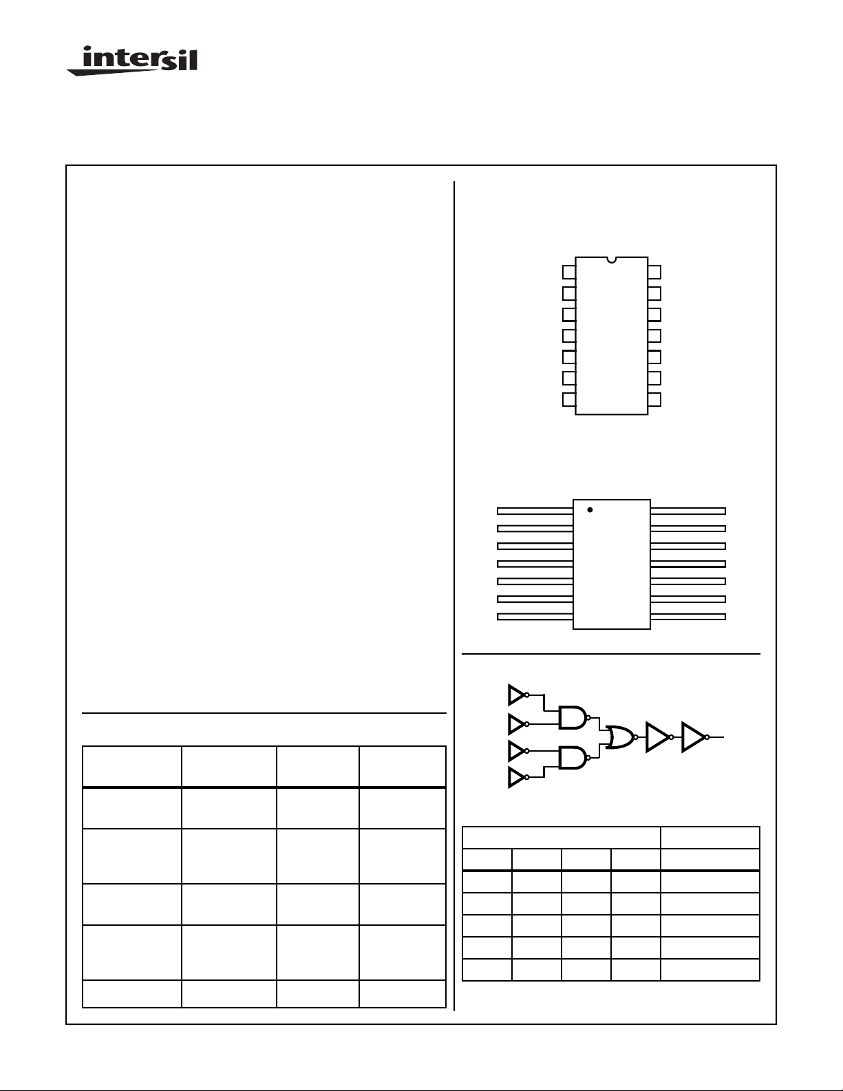
The HCTS4002MS is supplied in a 14 lead Ceramic flatpack (K
suffix) or a SBDIP Package (D suffix).
Pinouts
14 LEAD CERAMIC DUAL-IN-LINE METAL SEAL
PACKAGE (SBDIP) MIL-STD-1835 CDIP2-T14
TOP VIEW
Y1
1
2
A1
3
B1
4
C1
5
D1
6
NC
7
GND
14 LEAD CERAMIC METAL SEAL FLATPACK PACKAGE
(FLATPACK) MIL-STD-1835 CDFP3-F14
TOP VIEW
1Y1
A1
B1
C1
D1
NC
GND
2
3
4
5
6
7
14
VCC
13
Y2
12
D2
11
C2
10
B2
9
A2
8
NC
14
13
12
11
10
9
8
VCC
Y2
D2
C2
B2
A2
NC
Functional Diagram
An
Ordering Information
PART
NUMBER
HCTS4002DMSR -55oC to +125oC Intersil Class
HCTS4002KMSR -55oC to +125oC Intersil Class
HCTS4002D/
Sample
HCTS4002K/
Sample
HCTS4002HMSR +25oC Die Die
CAUTION: These devices are sensitive to electrostatic discharge; follow proper IC Handling Procedures.
http://www.intersil.com or 407-727-9207
TEMPERATURE
RANGE
+25oC Sample 14 Lead SBDIP
+25oC Sample 14 Lead
| Copyright © Intersil Corporation 1999
SCREENING
LEVEL PACKAGE
14 Lead SBDIP
S Equivalent
14 Lead
S Equivalent
Ceramic
Flatpack
Ceramic
Flatpack
718
Bn
Cn
Dn
An Bn Cn Dn Yn
LLLL H
HXXX L
XHXX L
XXHX L
XXXH L
NOTE: L = Logic Level Low, H = Logic level High,
TRUTH TABLE
INPUTS OUTPUTS
X = Don’t Care
Spec Number
File Number 3075.1
Yn
518632
Specifications HCTS4002MS
Absolute Maximum Ratings Reliability Information
Supply Voltage (VCC). . . . . . . . . . . . . . . . . . . . . . . . . . -0.5 to +7.0V
Input Voltage Range, All Inputs . . . . . . . . . . . . .-0.5V to VCC +0.5V
DC Input Current, Any One Input . . . . . . . . . . . . . . . . . . . . . . . .±10mA
DC Drain Current, Any One Output. . . . . . . . . . . . . . . . . . . . . . .±25mA
(All Voltage Reference to the VSS Terminal)
Storage Temperature Range (TSTG) . . . . . . . . . . . -65oC to +150oC
Lead Temperature (Soldering 10sec) . . . . . . . . . . . . . . . . . . +265oC
Junction Temperature (TJ) . . . . . . . . . . . . . . . . . . . . . . . . . . +175oC
ESD Classification . . . . . . . . . . . . . . . . . . . . . . . . . . . . . . . . Class 1
CAUTION: As with all semiconductors, stress listed under “Absolute Maximum Ratings” may be applied to devices (one at a time) without resulting in permanent
damage. This is a stress rating only. Exposure to absolute maximum rating conditions for extended periods may affect device reliability. The conditions listed
under “Electrical Performance Characteristics” are the only conditions recommended for satisfactory device operation..
Operating Conditions
Supply Voltage (VCC). . . . . . . . . . . . . . . . . . . . . . . . +4.5V to +5.5V
Operating Temperature Range (TA) . . . . . . . . . . . . -55oC to +125oC
Input Rise and Fall Times at 4.5V VCC (TR, TF). . . . . . .500ns Max
TABLE 1. DC ELECTRICAL PERFORMANCE CHARACTERISTICS
Thermal Resistance θ
SBDIP Package. . . . . . . . . . . . . . . . . . . . 74oC/W 24oC/W
Ceramic Flatpack Package . . . . . . . . . . . 116oC/W 30oC/W
Maximum Package Power Dissipation at +125oC Ambient
SBDIP Package. . . . . . . . . . . . . . . . . . . . . . . . . . . . . . . . . .0.68W
Ceramic Flatpack Package . . . . . . . . . . . . . . . . . . . . . . . . . 0.43W
If device power exceeds package dissipation capability, provide heat
sinking or derate linearly at the following rate:
SBDIP Package. . . . . . . . . . . . . . . . . . . . . . . . . . . . . .13.5mW/oC
Ceramic Flatpack Package . . . . . . . . . . . . . . . . . . . . . .8.6mW/oC
Input Low Voltage (VIL). . . . . . . . . . . . . . . . . . . . . . . . . 0.0V to 0.8V
Input High Voltage (VIH). . . . . . . . . . . . . . . . . . . . . . .VCC/2 to VCC
JA
θ
JC
(NOTE 1)
PARAMETER SYMBOL
Quiescent Current ICC VCC = 5.5V,
Output Current
(Sink)
Output Current
(Source)
Output Voltage Low VOL VCC = 4.5V, VIH = 2.25V,
Output Voltage High VOH VCC = 4.5V, VIH = 2.25V,
Input Leakage
Current
IOL VCC = 4.5V, VIH = 4.5V,
IOH VCC = 4.5V, VIH = 4.5V,
IIN VCC = 5.5V, VIN = VCC or
CONDITIONS
VIN = VCC or GND
VOUT = 0.4V, VIL = 0V
VOUT = VCC -0.4V,
VIL = 0V
IOL = 50µA, VIL = 0.8V
VCC = 5.5V, VIH = 2.75V,
IOL = 50µA, VIL = 0.8V
IOH = -50µA, VIL = 0.8V
VCC = 5.5V, VIH = 2.75V,
IOH = -50µA, VIL = 0.8V
GND
GROUP
A SUB-
GROUPS TEMPERATURE
1 +25oC-10µA
2, 3 +125oC, -55oC - 200 µA
1 +25oC 4.8 - mA
2, 3 +125oC, -55oC 4.0 - mA
1 +25oC -4.8 - mA
2, 3 +125oC, -55oC -4.0 - mA
1, 2, 3 +25oC, +125oC, -55oC - 0.1 V
1, 2, 3 +25oC, +125oC, -55oC - 0.1 V
1, 2, 3 +25oC, +125oC, -55oC VCC
1, 2, 3 +25oC, +125oC, -55oC VCC
1 +25oC-±0.5 µA
2, 3 +125oC, -55oC-±5.0 µA
LIMITS
-V
-0.1
-V
-0.1
UNITSMIN MAX
Noise Immunity
Functional Test
NOTES:
1. All voltages reference to device GND.
2. For functional tests VO ≥ 4.0V is recognized as a logic “1”, and VO ≤ 0.5V is recognized as a logic “0”.
FN VCC = 4.5V, VIH = 2.25V,
VIL = 0.8V (Note 2)
7, 8A, 8B +25oC, +125oC, -55oC---
719
Spec Number 518632
Specifications HCTS4002MS
TABLE 2. AC ELECTRICAL PERFORMANCE CHARACTERISTICS
GROUP
(NOTES 1, 2)
PARAMETER SYMBOL
Input to Output TPHL,
TPLH
NOTES:
1. All voltages referenced to device GND.
2. AC measurements assume RL = 500Ω, CL = 50pF, Input TR = TF = 3ns, VIL = GND, VIH = 3V.
TABLE 3. ELECTRICAL PERFORMANCE CHARACTERISTICS
PARAMETER SYMBOL CONDITIONS NOTES TEMPERATURE
Capacitance Power
Dissipation
Input Capacitance CIN VCC = Open, f = 1MHz 1 +25oC - 10 pF
Output Transition
Time
NOTE:
1. The parameters listed in Table 3 are controlled via design or process parameters. Min and Max Limits are guaranteed but not directly
tested. These parameters are characterized upon initial design release and upon design changes which affect these characteristics.
CPD VCC = 5.0V, f = 1MHz 1 +25oC - 38 pF
TTHL
TTLH
CONDITIONS
VCC = 4.5V 9 +25oC 2 22 ns
VCC = 4.5V 1 +25oC - 15 ns
A SUB-
GROUPS TEMPERATURE
10, 11 +125oC, -55oC 2 25 ns
1 +125oC - 47 pF
1 +125oC - 10 pF
1 +125oC - 22 ns
LIMITS
UNITSMIN MAX
LIMITS
UNITSMIN MAX
TABLE 4. DC POST RADIATION ELECTRICAL PERFORMANCE CHARACTERISTICS
200K RAD
(NOTES 1, 2)
PARAMETER SYMBOL
Quiescent Current ICC VCC = 5.5V, VIN = VCC or GND +25oC - 0.2 mA
Output Current (Sink) IOL VCC = 4.5V, VIN = VCC or GND,
VOUT = 0.4V
Output Current (Source) IOH VCC = 4.5V, VIN = VCC or GND,
VOUT = VCC -0.4V
Output Voltage Low VOL VCC = 4.5V or 5.5V, VIH = VCC/2,
VIL = 0.8V , IOL = 50µA
Output Voltage High VOH VCC = 4.5V or 5.5V, VIH =VCC/2,
VIL = 0.8V, IOH = -50µA
Input Leakage Current IIN VCC = 5.5V, VIN = VCC or GND +25oC-±5 µA
Noise Immunity
Functional Test
Input to Output TPHL,
NOTES:
1. All voltages referenced to device GND.
2. AC measurements assume RL = 500Ω, CL = 50pF, Input TR = TF = 3ns, VIL = GND, VIH = 3V.
3. For functional tests VO ≥ 4.0V is recognized as a logic “1”, and VO ≤ 0.5V is recognized as a logic “0”.
FN VCC = 4.5V, VIH = 2.25V,
VIL = 0.8V at 200K RAD,
(Note 3)
VCC = 4.5V +25oC 2 25 ns
TPLH
CONDITIONS TEMPERATURE
+25oC 4.0 - mA
+25oC -4.0 - mA
+25oC - 0.1 V
+25oC VCC
+25oC ---
LIMITS
UNITSMIN MAX
-V
-0.1
720
Spec Number 518632
 Loading...