


HC-5560
Data Sheet January 1997 File Number
PCM Transcoder
The HC-5560 digital line transcoder provides encoding and
decoding of pseudo ternary line code substitution schemes.
Unlike other industry standard transcoders, the HC-5560
provides four worldwide compatible mode selectable code
substitution schemes, including HDB3 (High Density Bipolar
3), B6ZS, B8ZS (Bipolar with 6 or 8 Zero Substitution) and
AMI (Alternate Mark Inversion).
The HC-5560 is fabricated in CMOS and operates from a
single 5V supply. All inputs and outputs are TTL compatible.
Application Note #573, “The HC-5560 Digital Line
Transcoder,” by D.J. Donovan is available.
Ordering Information
PART
NUMBER
HC3-5560-5 0 to 70 20 Ld PDIP E20.3
TEMP.RANGE
(oC) PACKAGE PKG. NO.
Pinout
HC-5560
(PDIP)
TOP VIEW
FORCE AIS
MODE SELECT 1
NRZ DATA IN
CLK ENC
MODE SELECT 2
NRZ DATA OUT
CLK DEC
RESET AIS
AIS
V
SS
1
2
3
4
5
6
7
8
9
10
V
20
DD
OUTPUT ENABLE
19
RESET
18
OUT1
17
OUT2
16
B
15
IN
LOOP TEST ENABLE
14
A
13
IN
12
CLOCK
11
ERROR
2887.2
Features
• Single 5V Supply . . . . . . . . . . . . . . . . . . . . . . .10mA (Typ)
• Mode Selectable Coding Including:
- AMI (T1, T1C)
- B8ZS (T1)
- HDB3 (PCM30)
• North American and European Compatibility
• Simultaneous Encoding and Decoding
• Asynchronous Operation
• Loop Back Control
• Transmission Error Detection
• Alarm Indication Signal
• Replaces MJ1440, MJ1471 and TCM2201 Transcoders
Applications
• North American and European PCM Transmission Lines
where Pseudo Ternary Line Code Substitution Schemes
are Desired
• Any Equipment that Interfaces T1, T1C, T2 or PCM30
Lines Including Multiplexers, Channel Service Units,
(CSUs) Echo Cancellors, Digital Cross-Connects (DSXs),
T1 Compressors, etc.
• Related Literature
- AN573, The HC-5560 Digital Line Transcoder
Functional Diagram
MODE
SELECT
NRZ DATA IN
CLK ENC
OUTPUT
ENABLE
1
2
TRANSMITTER/
ENCODER
V
DD
V
SS
CLOCK
OUT 1
OUT 2
69
LOOP TEST
ENABLE
A
IN
B
IN
FORCE AIS
RESET
CLK DEC
RESET AIS
CAUTION: These devices are sensitive to electrostatic discharge; follow proper IC Handling Procedures.
http://www.intersil.com or 407-727-9207 | Copyright © Intersil Corporation 1999
SWITCH
AIS
DETECT
RECEIVER/
DECODER
ERROR
DETECT
NRZ DAT A
OUT
ERROR
AIS

HC-5560
Absolute Maximum Ratings Thermal Information
Voltage at Any Pin . . . . . . . . . . . . . . . . . . . .GND -0.3V to VDD 0.3V
Maximum VDD Voltage . . . . . . . . . . . . . . . . . . . . . . . . . . . . . . . 7.0V
Operating Conditions
Operating Temperature Range . . . . . . . . . . . . . . . . . . . 0oC to 70oC
Operating VDD. . . . . . . . . . . . . . . . . . . . . . . . . . . . . . . . . . . 5V ±5%
CAUTION: Stresses above those listed in “Absolute Maximum Ratings” may cause permanent damage to the device. This is a stress only rating and operationofthe
device at these or any other conditions above those indicated in the operational sections of this specification is not implied.
NOTES:
1. θJA is measured with the component mounted on an evaluation PC board in free air.
Thermal Resistance (Typical, Note 1) θJA (oC/W)
PDIP Package . . . . . . . . . . . . . . . . . . . . . . . . . . . . . 67
Maximum Junction Temperature . . . . . . . . . . . . . . . . . . . . . . .175oC
Maximum Junction Temperature (Plastic Package). . . . . . . . .150oC
Storage Temperature Range . . . . . . . . . . . . . . . . . . -65oC to 150oC
Maximum Lead Temperature (Soldering 10s) . . . . . . . . . . . . . . 300
Die Characteristics
Transistor Count. . . . . . . . . . . . . . . . . . . . . . . . . . . . . . . . . . . . .4322
Die Dimensions . . . . . . . . . . . . . . . . . . . . . . . . . .119 mils x 133 mils
Substrate Potential. . . . . . . . . . . . . . . . . . . . . . . . . . . . . . . . . . . . .+V
Process . . . . . . . . . . . . . . . . . . . . . . . . . . . . . . . . . . . . . SAJI CMOS
o
Electrical Specifications Unless Otherwise Specified, Typical parameters at 25
o
C, Min-Max parameters are over operating
temperature range. VDD = 5V
PARAMETER SYMBOL MIN TYP MAX UNITS
STATIC SPECIFICATIONS
Quiescent Device Current l
DD
100 µA
Operating Device Current 10 mA
OUT1, OUT2 Low (Sink) Current
I
OL1
3.2 mA
(VOL = 0.4V)
All Other Outputs Low (Sink) Current
I
OL2
2mA
(VOL = 0.8V)
All Outputs High (Source) Current
I
OH
2mA
(VOH = 4V)
Input Low Current I
Input High Current I
Input Low Voltage V
Input High Voltage V
Input Capacitance C
IL
IH
lL
lH
lN
Electrical Specifications Unless Otherwise Specified, Typical parameters at 25
2.4 V
o
C, Min-Max parameters are over operating
10 µA
10 µA
0.8 V
8pF
temperature range. VDD = 5V
PARAMETER SYMBOL FIGURE MIN TYP MAX UNITS
DYNAMIC SPECIFICATIONS
CLK ENC, CLK DEC Input Frequency f
CLK ENC,CLK DEC Rise Time (1.544MHz) t
Fall Time t
Rise Time (2.048MHz) t
Fall Time t
Rise Time (6.3212MHz) t
Fall Time t
Rise Time (8.448MHz) t
Fall Time t
70
CL
RCL
FCL
RCL
FCL
RCL
FCL
RCL
FCL
8.5 MHz
1, 2 10 60 ns
1, 2 10 60 ns
1, 2 10 40 ns
1, 2 10 40 ns
1, 2 10 30 ns
1, 2 10 30 ns
1, 2 5 10 ns
1, 2 5 10 ns

HC-5560
Electrical Specifications Unless Otherwise Specified, Typical parameters at 25
temperature range. VDD = 5V (Continued)
PARAMETER SYMBOL FIGURE MIN TYP MAX UNITS
NRZ-Data In to CLK ENC Data Setup Time t
Data Hold Time t
AIN, BIN to CLK DEC Data Setup Time t
Data Hold Time t
CLK ENC to OUT1, OUT2 t
OUT1, OUT2 Pulse Width (CLK ENC Duty Cycle = 50%)
fCL = 1.544MHz t
fCL = 2.048MHz t
fCL = 6.3212MHz t
f
= 8.448MHz t
CL
CLK DEC to NRZ-Data Out t
Setup Time CLK DEC to Reset AlS t
Hold Time of Reset AlS = ‘0’ t
Setup Time Reset AlS = ‘1’ to CLK DEC t
Reset AlS to AIS output t
CLK DEC to Error output t
S
H
S
H
DD
W
W
W
W
DD
S2
H2
S2
PD5
PD4
o
C, Min-Max parameters are over operating
120--ns
120--ns
215--ns
25--ns
1 - 23 80 ns
1 - 324 - ns
1 - 224 - ns
1 - 79 - ns
1 - 58 - ns
2 - 25 54 ns
335--ns
320--ns
30--ns
3--42ns
3--62ns
Pin Descriptions
PIN NUMBER FUNCTION DESCRIPTION
1 Force AIS Pin 19must be at logic ‘0’ to enable this pin. A logic ‘1’ on this pin forces OUT1 and OUT2to all ‘1’s.A logic
‘0’ on this pin allows normal operation.
2, 5 Mode Select 1,
Mode Select 2
3 NRZ Data In Input data to be encoded into ternary form. The data is clocked by the negative going edge of CLK ENC.
4 CLK ENC Clock encoder, clock for encoding data at NRZ Data In.
6 NRZ Data Out Decoded data from ternary inputs AIN and BIN.
7 CLK DEC Clock decoder, clock for decoding ternary data on inputs AIN and BIN.
8, 9 Reset AIS, AlS Logic ‘0’ onReset AIS resetsa decodedzero counter andeither resets AISoutput tozero provided 3or more
10 V
SS
11 Error A logic ‘1’ indicates that a violation of the line coding scheme has been decoded.
12 Clock “OR” function of AIN and BIN for clock regeneration when pin 14 is at logic ‘0’, “OR” function of OUT1 and
13, 15 AIN, B
IN
MS1 MS2 Functions As
0 0 AMI
0 1 B8ZS
1 0 B6ZS
1 1 HDB3
zeros have been decodedin thepreceding Reset AIS period or sets AlSto ‘1’if less than 3 zeros have been
decoded in the preceding two Reset AlS periods. A period of Reset AlS is defined from the bit following the
bit during which Reset AlS makes a high to low transition to the bit during which Reset AIS makes the next
high to low transition.
Ground reference.
OUT2 when pin 14 is at logic ‘1’.
Inputsrepresenting thereceivedPCM signal. AIN=‘1’ representsapositive going ‘1’and BIN=‘1’ represents
a negative going ‘1’. AINand BINare sampled by the positive going edge of CLK DEC. AINand BINmay be
interchanged.
71

HC-5560
Pin Descriptions
PIN NUMBER FUNCTION DESCRIPTION
14 LTE Loop Test Enable, this pin selects between normal and loop back operation. A logic ‘0’ selects normal oper-
16, 17 OUT1, OUT2 Outputs representing the ternary encoded NRZ Data In signal for line transmission. OUT1 and OUT2 are in
18 Reset A logic ‘0’ on this pin resets all internal registers to zero. A logic ‘1’ allows normal operation of all internal
19 Output Enable A logic ‘1’ on this pin forces outputs OUT1 and OUT2 to zero. A logic ‘0’ allows normal operation.
20 V
Functional Description
(Continued)
DD
ation where encodeand decode areindependent and asynchronous.A logic‘1’selects aloop back condition
where OUT1 is internally connected to AIN and OUT2 is internally connected to BIN. A decode clock must
be supplied.
return to zero form and are clocked out on the positive going edge of CLK ENC. The length of OUT1 and
OUT2 is set by the length of the positive clock pulse.
registers.
Power to chip.
level at the Alarm Indication Signal (AlS) output. This is also
known as Blue Code. The AlS output is set to a high level
The HC-5560 TRANSCODER can be divided into six sections: transmission (coding), reception (decoding), error
detection, all ones detection, testing functions, and output
controls.
The transmitter codes a non-return to zero (NRZ) binary unipolar input signal (NRZ Data In) into two binary unipolar
return to zero (RZ) output signals (OUT1, OUT2). These output signals represent the NRZ data stream modified according to the selected encoding scheme (i.e.,AMl, B8ZS, B6ZS,
HDB3) and are externally mixed together (usually via a transistor or transformer network) to create a ternary bipolar signal for driving transmission lines.
The receiver accepts as its input the ternary data from the
transmission line that has been externally split into two
binary unipolar return to zero signals (A
and BIN). These
IN
when less than threezeros are received during one period of
Reset AIS immediately followed by another period of Reset
AlS containing less than three zeros. The AIS output is reset
to a low level upon the first period of
Reset AlS containing 3
or more zeros.
A logic high level on LTE enables a loopback condition
where OUT1 is internally connected to A
internally connected to B
(this disables inputs AINand B
IN
and OUT2 is
IN
to external signals). In this condition, NRZ Data In appears
at NRZ Data Out (delayed by the amount of clock cycles it
takes to encode and decode the selected line code). A
decode clock must be supplied for this operation.
The output controls are
Output Enable and Force AlS. These
pins allow normal operation, force OUT1 and OUT2 to zero,
or force OUT1 and OUT2 to output all ones (AIS condition).
signals are decoded, according to the rules of the selected
line code into one binary unipolar NRZ output signal (NRz
Data Out).
The encoder and decoder sections of the chip perform independently (excluding loopback condition) and may operate
simultaneously.
The Error output signal is active high for one cycle of CLK
DEC upon the detection of any bipolar violation in the
received A
and BINsignals that is not part of the selected
IN
line coding scheme. The bipolar violation is not removed,
however , and shows up as a pulse in the NRZ Data Out signal. In addition, the Error output signal monitors the received
A
and BINsignals for a string of zeros that violates the
IN
Line Code Descriptions
AMl, Alternate Mark Inversion, is used primarily in North
American T1 (1.544MHz) and T1C (3.152MHz) carriers.
Zeros are coded as the absence of a pulse and ones are
coded alternately as positive or negative pulses. This type of
coding reduces the averagevoltage level to zero to eliminate
DC spectral components, thereby eliminating DC wander.To
simplify timing recovery, logic 1’s are encoded with 50% duty
cycle pulses.
e.g.,
PCM CODE
0100 0 0 00000111 1 1
maximum consecutive zeros allowed for the selected line
coding scheme (i.e., 15 for AMI, 8 for B8ZS, 6 for B6ZS, and
AMI CODE
4 for HDB3). ln the event that an excessive amount of zeros
is detected, the Error output signal will be active high for one
cycle of CLK DEC during the zero that exceeds the maximum number. In the case that a high level should simultaneously appear on both received input signals A
and BINa
IN
logical one is assumed and appears on the NRZ Data Out
stream with the Error output active.
An input signal received at inputs A
and BINthat consists
IN
of all ones (or marks) is detected and signaled by a high
To facilitate timing maintenance at regenerative repeaters
along a transmission path, a minimum pulse density of logic
1s is required. UsingAMl, there is a possibility of long strings
of zeros and the required density may not always exist, leading to timing jitter and therefore higher error rates.
A method for insuring minimum logic 1 density by substituting
bipolar code in place of strings of 0s is called BNZS or Bipolar
IN
72

HC-5560
with N Zero Substitution. B6ZS is used commonly in North
American T2 (6.3212MHz) carriers. For every string of 6
zeros, bipolar code is substituted according to the following
rule:
If the immediate preceding pulse is of (-) polarity, then
code each group of 6 zeros as 0+- 0+-, and if the
immediate preceding pulse is of (+) polarity,code each
group of 6 zeros as 0+- 0-+.
One can see the consecutive logic 1 pulses of the same
polarity violate the AMI coding scheme.
e.g.,
6
PCM CODE
-)
B6ZS (
B6ZS (+)
0100 0 000000111 1
V = VIOLATION
-
00
V
+
00
V
-
++
V
+
--
V
B8ZS is used commonly in North American T1 (1.544MHz)
and T1C (3.152MHz) carriers. For every string of 8 zeros,
bipolar code is substituted according to the following rules:
1. If the polarity of the immediate preceding pulse is (-)
and there have been an odd (even) number of logic 1
pulses since the last substitution, each group of 4 consecutive zeros is coded as 000-(+00+).
2. If the polarity of the immediate preceding pulse is (+)
then the substitution is 000+(-00-) for odd (even) number of logic 1 pulses since the last substitution.
e.g.,
44
PCM CODE
HDB3 (-)
HDB3 (+)
01000 0 000000
V
000 00
+
V
111 1
- +
V = VIOLATION
+
00000
V
--
V
The 3 in HDB3 refers to the coding format that precludes
strings of zeros greater than 3. Note that violations are produced only in the fourth bit location of the substitution code
and that successive substitutions produce alternate polarity
violations.
1. If the immediate preceding pulse is of (-) polarity, then
code each group of 8 zeros as 000-+ 0+-.
2. If the immediate preceding pulse is of (+) polarity then
code each group of 8 zeros as 000+-0-+.
e.g.,
8
PCM CODE
B8ZS (-)
B8ZS (+)
11 110 00000000 0
++
0000
-
V
000 0
++
V
V = VIOLATION
-
V
--
The BNZS coding schemes, in addition to eliminating DC
wander, minimize timing jitter and allow a line error monitoring capability.
Another coding scheme is HDB3, high density bipolar 3, used
primarily in Europe f or2.048MHz and 8.448MHz carriers.This
code is similar to BNZS in that it substitutes bipolar code for 4
consecutive zeros according to the follo wing rule:
73

Application Diagram
FROM CODEC OR
TRANSCODER
ENCODER CLOCK
HC-5560
5V
V
DD
NRZ DATA IN
ENCODER
CLK ENC OUT2
OUT1
V+
T1, T2, T1C,
PCM 30
LINE OUTPUT
LINE
INPUT
DIFF
AMP
Timing Waveforms
V+
±
±
t
RCL
CLK ENC
FORCE AIS MS1
LTE
RESET
OUTPUT
ENABLE
A
IN
B
IN
CLK DEC V
DECODER CLOCK
10%
CONTROL
DECODER
1
f
CL
t
S
90%
MS2
CLOCK
RESET AIS
AIS
ERROR
NRZ DATA OUT
SS
t
FCL
50%
MODE SELECT
LOGIC INPUTS
CLOCK RECOVERY
ALARM CLOCK
ALARM
ERROR
TO CODED OR TRANSCODER
MS1 MS2 SELECTS
0
0
1
t
H
ERROR
MONITORS
0
1
0
AMI
B8ZS
B6ZS
HDB311
NRZ DATA IN
OUT 1, OUT 2
74
50%50%
t
DD
50% 50%
t
W
FIGURE 1. TRANSMITTER (CODER) TIMING WAVEFORMS

HC-5560
Timing Waveforms
(Continued)
t
FCL
CLK DEC
, B
A
IN
CLOCK
NRZ DATA OUT
FIGURE 2. RECEIVER (DECODER) TIMING WAVEFORMS
1
f
CL
t
RCL
90%
10%
t
S
IN
50%
50%
t
DD
50%
50%
t
H
CLK DEC
RESET AIS
NRZ DATA OUT
AIS
CLK DEC
RESET AIS
AIS OUTPUT
ERROR OUTPUT
50% 50%
t
H2
50% 50%
t
t
PD5
S2
50%
t
PD4
50%
FIGURE 3. RESET AIS INPUT, AIS OUTPUT, ERROR OUTPUT
t
S2
FIGURE 4.
Two consecutiveperiodsof Reset AIS, each containing less than three zeros, sets AIS to a logic ‘1’ and remains in a logic ‘1’ state
until a period of
Reset AIS contains three or more zeros.
75
HC-5560
Timing Waveforms
CLK DEC
RESET AIS
NRZ DATA OUT
AIS
(Continued)
FIGURE 5.
Zeros which occur during a high to low transition of Reset AIS are counted with the zeros that occurred before the high to low transition.
NRZ DATA IN
CLK ENC
OUT 1
AMI
OUT 2
HDB3
B6ZS
B8ZS
OUT 1
OUT 2
OUT 1
OUT 2
OUT 1
OUT 2
SS S
SS
S
3 1/2 CYCLES
5 1/2 CYCLES
SS
SS
SS
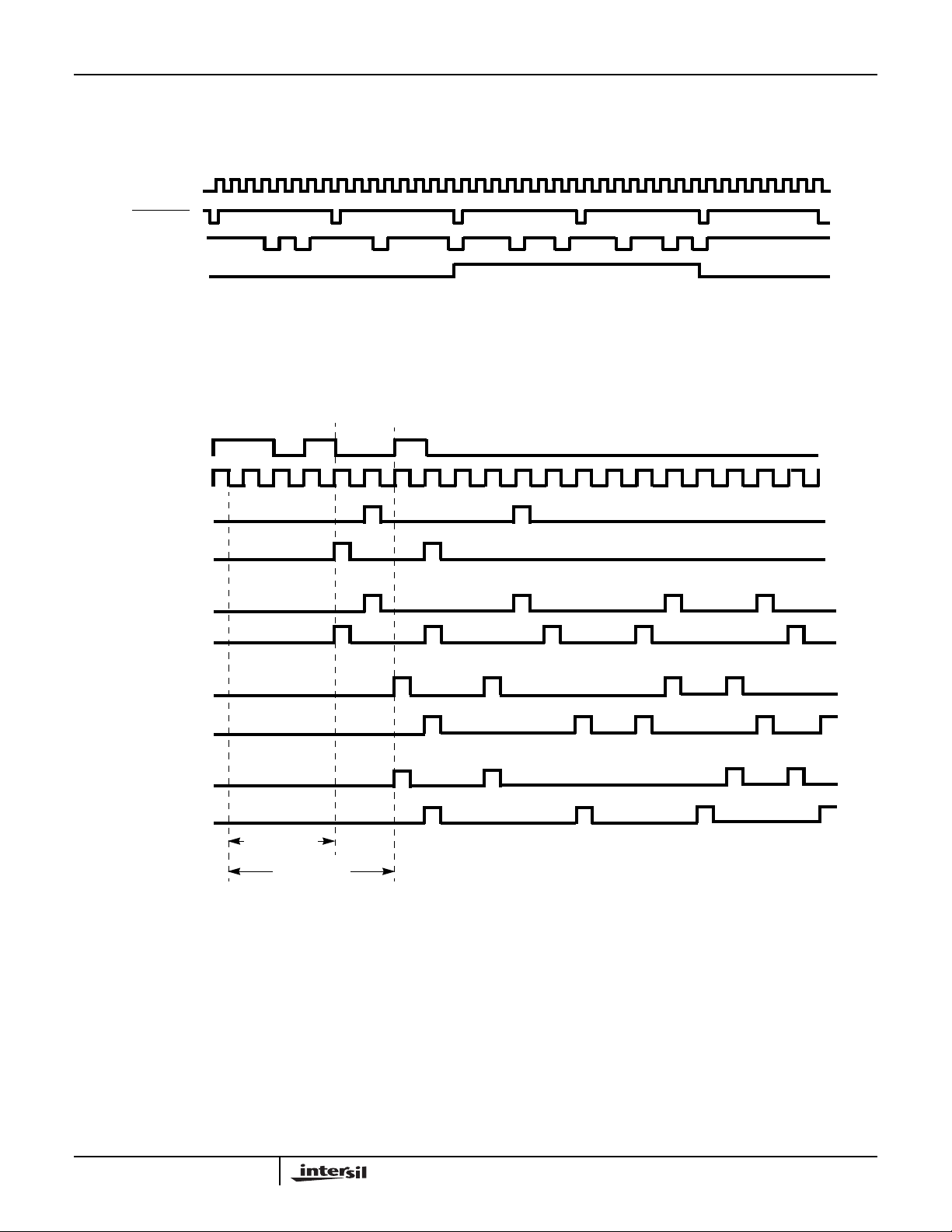
FIGURE 6. ENCODE TIMING AND DELAY
Data is clocked on the negative edge of CLK ENC and appears on OUT1 and OUT2. OUT1 and OUT2 are interchangeable. Bipolar violations and all other pulses inserted by the line coding scheme to encode strings of zeros are labeled with an “S”.
76

HC-5560
Timing Waveforms
CLK DEC
A
AMI
NRZ DATA OUT
HDB3
NRZ DATA OUT
B6ZS
NRZ DATA OUT
B8ZS
NRZ DATA OUT
IN
B
IN
A
IN
B
IN
A
IN
B
IN
A
IN
B
IN
(Continued)
4 CYCLES
6 CYCLES
8 CYCLES
SS S S
SS SS
SSS
SSSS
S
SS
SSSSS
SSS
FIGURE 7. DECODE TIMING AND DELAY
Data that appears on AIN and BIN is clocked by the positive edge of CLK DEC, decoded, and zeros are inserted for all valid line
code substitutions. The data then appears in non-return to zero to zero form at output NRZ Data Out. A
and BIN are
IN
interchangeable.
CLK DEC
A
B
NRZ DATA
OUT
ERROR
IN
IN
E
EE
S
SS
S
FIGURE 8.
The ERROR signal indicates bipolar violations that are not part of a valid substitution.
All Intersil semiconductor products are manufactured, assembled and tested under ISO9000 quality systems certification.
Intersil semiconductor products are sold by description only. Intersil Corporation reserves the right to make changes in circuit design and/or specifications at any time without notice. Accordingly, the reader is cautioned to verify that data sheets are current before placing orders. Information furnished by Intersil is believed to be accurate and
reliable. However, no responsibility is assumed by Intersil or its subsidiaries forits use; nor for any infringements of patents or other rights of third parties which may result
from its use. No license is granted by implication or otherwise under any patent or patent rights of Intersil or its subsidiaries.
For information regarding Intersil Corporation and its products, see web site http://www.intersil.com
77
 Loading...