Semiconductor
HC5549
Data Sheet January 1999 File Number
Low Power SLIC with Battery Switch
The HC5549 Subscriber line
interface circuit is a 100V
diellectrically isolated bipolar
integrated circuit for use in
short loop ISDN, P ABX and
Pairgain applications. The HC5549 has been optimized for low
power as required for battery backed remote terminals or for
applications requiring emergency powering from the line such
as European ISDN NT1+ designs.
A high and low voltage battery supply may be connected to
the HC5549 so that power dissipation can be lowered in the
off hook condition in these short loop applications. The high
battery supply can beused in the on-hook condition to allow
interfacing to fax and answering machines that require 48V
to detect end of call status. The HC5549 also has a low
power standby state with very low power consumption
(35mW) resulting in exceptionally low battery drain while
providing continued loop supervision.
The HC5549 provides loop current, ground key and ring trip
detect functions as well as an alarm output to indicate
thermal overload.
2-wire to 4-wire and 4-wire to 2-wire conversion is provided
and impedance matching is achievedusing a single external
network. The HC5549 is compatible with dual and single
supply switched capacitor or DSP codec/filters
Features
• Dual Battery Operation
• Single Additional +5V Supply
• Low Standby Power Consumption (48V, 35mW)
• On Hook Transmission
• Tip and Ring Disconnect
• Soft or Hard Polarity Reversal
• Supports 12 kHz or 16 kHz Pulse Metering
• Ring Relay Driver
• On Chip 2-wire AC/DC Loopback
• No Latch-Up or Power Supply Sequencing
o
to 70o or -40o to 85o Ambient Temp Range
•0
• Low External Component Count
Applications
• ISDN NT1+ Terminals
• Pairgain Remote Termination
• PABX and Key Systems
Related Literature
• AC SPICE Macromodel
4539.1
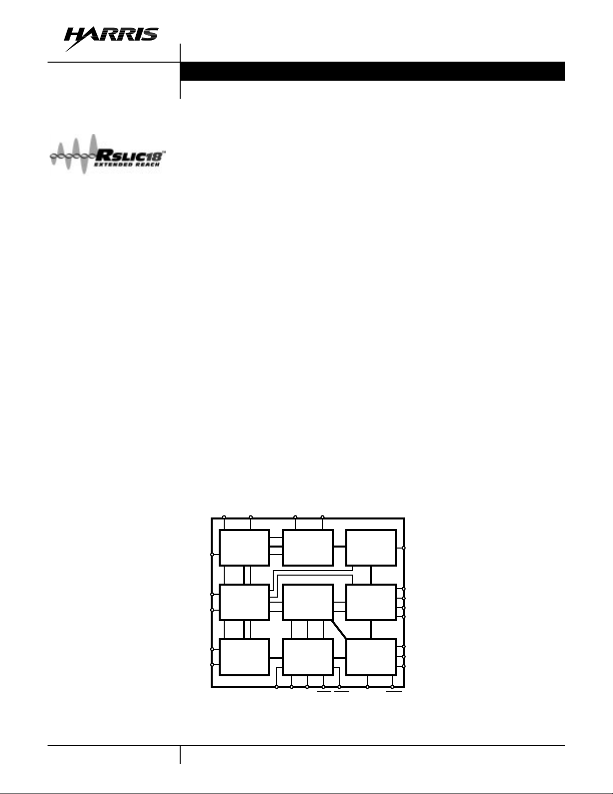
Block Diagram
4-80
POL CDC VBHVBL
DC
ILIM
TIP
RING
SW+
SW-
CONTROL
2-WIRE
PORT
TEST
ACCESS
BATTERY
SWITCH
TRANSMIT
SENSING
DETECTOR
LOGIC
RTD RD
CAUTION: These devices are sensitive to electrostatic discharge; follow proper IC Handling Procedures.
E0
DET ALM
RINGING
PORT
4-WIRE
PORT
CONTROL
LOGIC
BSEL
1-800-4-HARRIS or 407-727-9207
VRS
VRX
VTX
-IN
VFB
F2
F1
F0
SWC
RSLIC18™ is a trademark of Harris Corporation.
| Copyright © Harris Corporation 1999

HC5549
Ordering Information (PLCC Package Only)
BATSWPOL
PART NUMBER 48V
HC5549CM ••
HC5549IM
•
•
REV
•
•
RING
DELAY
DRIVER
•
•
2W
LOOP
BACK LB = 53dB
••
••
TEMP.
RANGEoC PACKAGE
PACKAGE
NO.
0 to 70 28 Ld PLCC N28.45
-40 to 85 28 Ld PLCC N28.45
Device Operating Modes
OPERATING MODE F2 F1 F0 E0 = 1 E0 = 0 DESCRIPTION
Low Power Standby 0 0 0 SHD GKD MTU compliant standby mode with active loop
detector.
Forward Active 0 0 1 SHD GKD Forward battery loop feed.
Unused 0 1 0 n/a n/a Reserved internal test mode.
Reverse Active 0 1 1 SHD GKD Reverse battery loop feed.
Ringing 1 0 0 RTD RTD Enabler internal ring trip detector.
Unused 1 0 1 n/a n/a Reserved internal test mode.
Unused 1 1 0 n/a n/a Reserved internal test mode.
Power Denial 1 1 1 n/a n/a Device shutdown.
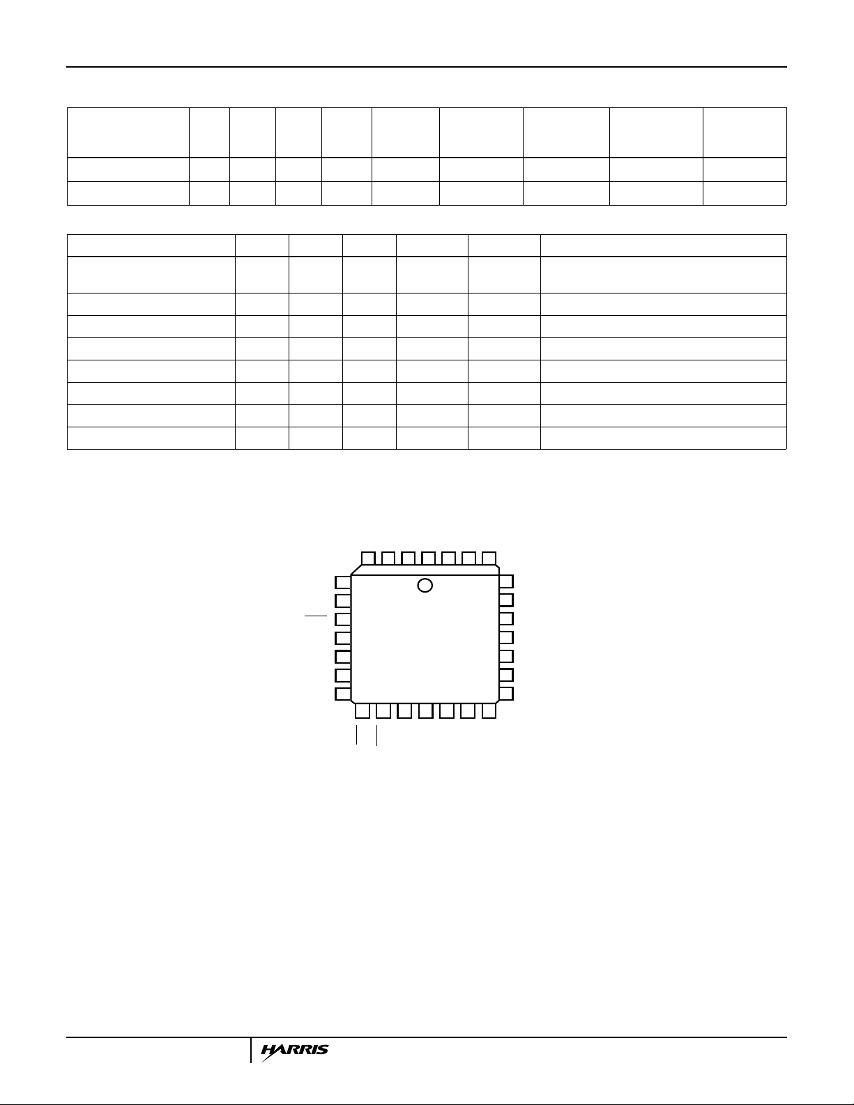
Pinouts
HC5549 (PLCC)
TOP VIEW
SW+
SW-
SWC
F2
F1
F0
E0
RD
RING
NC
ILIM
27
26
RTD
25
CDC
24
V
23
CC
22
-IN
VFB
21
VTX
20
VRX
19
17
18
VRB
POL
TIP
VBL
VBH
13
3
ALM
14
BGND
15
AGND
12
28
16
NC
4
5
6
7
8
9
10
11
12
DET
4-81

HC5549
Absolute Maximum Ratings T
Maximum Supply Voltages
VCC . . . . . . . . . . . . . . . . . . . . . . . . . . . . . . . . . . . . . -0.5V to +7V
VCC - V
Uncommitted Switch Voltage. . . . . . . . . . . . . . . . . . . . . . . . . . -80V
ESD (Human Body Model). . . . . . . . . . . . . . . . . . . . . . . . . . . . 500V
. . . . . . . . . . . . . . . . . . . . . . . . . . . . . . . . . . . . . . . 80V
BAT
Operating Conditions
Temperature Range
Industrial (I suffix). . . . . . . . . . . . . . . . . . . . . . . . . . -40oC to 85oC
Commercial (C suffix). . . . . . . . . . . . . . . . . . . . . . . . 0oC to 75oC
Positive Power Supply (VCC). . . . . . . . . . . . . . . . . . . . . . . +5V ±5%
Negative Power Supply (VBH, VBL) (180, 181, 182) . . -16V to -80V
Uncommitted Switch (loop back or relay driver). . . . . . . +5V to -80V
CAUTION: Stresses above those listed in “Absolute Maximum Ratings” may cause permanent damage to the device. This is a stress only rating and operationofthe
device at these or any other conditions above those indicated in the operational sections of this specification is not implied.
NOTE:
1. θJA is measured with the component mounted on an evaluation PC board in free air.
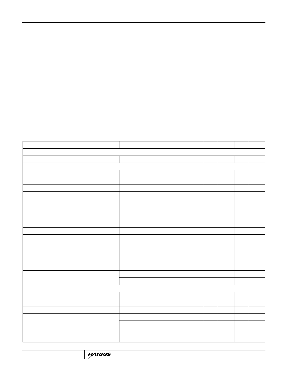
Electrical Specifications Unless Otherwise Specified, T
PARAMETER TEST CONDITIONS MIN TYP MAX UNITS
RINGING PARAMETERS
VRB Input Impedance 480 - - kΩ
AC TRANSMISSION PARAMETERS (Forward Active and Reverse Active, BSEL = 0, unless otherwise specified.)
Receive Input Impedance 160 - - kΩ
Transmit Output Impedance --1Ω
4-Wire Port Overload Level THD = 1% 3.1 3.5 - V
2-Wire Port Overload Level THD = 1% 3.1 3.5 - V
2-Wire Return Loss 300Hz ≤ f < 1kHz 30 45 - dB
Longitudinal Current Capability (Per Wire) Test for False Detect - 20 - mA
2-Wire Longitudinal Balance Tested per IEEE455-1985, with 368Ω per wire. 53 - - dB
4-Wire Longitudinal Balance Tested per IEEE455-1985, with 368Ω per wire. 59 - - dB
4-Wire to 4-Wire Insertion Loss -6.22 -6.02 -5.82 dB
2-Wire to 4-Wire Level Linearity
4-Wire to 2-Wire Level Linearity
Referenced to -10dBm
Idle Channel Noise 2-Wire C-Message - 16 19 dBrnC
DC PARAMETERS
Loop Current Limit Programming Range Max Low Battery = -52V, BSEL = 0 15 - 45 mA
Loop Current Accuracy I
Loop Current During Low Power Standby Forward polarity only. 17 - 26 mA
Open Circuit Voltage
(|Tip - Ring|)
Low Power Standby Open Circuit Voltage (Tip - Ring) BSEL = 1 43 45 47 V
Ring Trip Programming Current Accuracy - - 10 %
=25oC Thermal Information
A
Thermal Resistance (Typical, Note 1) θJA(oC/W)
PLCC Package. . . . . . . . . . . . . . . . . . . . . . . . . . . . . 53
Maximum Junction Temperature Plastic . . . . . . . . . . . . . . . . 150oC
Maximum Storage Temperature Range. . . . . . . . . . -65oC to 150oC
Maximum Lead Temperature (Soldering 10s) . . . . . . . . . . . . 300oC
(PLCC - Lead Tips Only)
Die Characteristics
Substrate Potential. . . . . . . . . . . . . . . . . . . . . . . . . . . . . . . . . . V
Process . . . . . . . . . . . . . . . . . . . . . . . . . . . . . . . . . . . . . . Bipolar-DI
= -40oC to 85oC, VBL = -24V, VBH= -48V, VCC = +5V, AGND = BGND = 0V , loop
current limit = 25mA. All AC Parameters are specified at 600Ω 2-wire terminating impedance over the frequency
band of 300Hz to 3.4kHz. Protection resistors = 0Ω.
A
PK
PK
1kHz ≤ f ≤ 3.4kHz 35 45 - dB
RMS
Test forFalseDetect,Low PowerStandby, BSEL=0 - 10 - mA
+3 to -40dBm, 1kHz - 0.025 - dB
-40 to -50dBm, 1kHz - 0.050 - dB
-50 to -55dBm, 1kHz - 0.100 - dB
Psophometric - -74 -71 dBmp
= 25mA, BSEL = 0 - - 10 %
L
BSEL = 0 14 15.5 17 V
BSEL = 1 37.5 40 42.5 V
RMS
BAT
4-82

HC5549
Electrical Specifications Unless Otherwise Specified, T
= -40oC to 85oC, VBL = -24V, VBH= -48V, VCC = +5V, AGND = BGND = 0V , loop
A
current limit = 25mA. All AC Parameters are specified at 600Ω 2-wire terminating impedance over the frequency
band of 300Hz to 3.4kHz. Protection resistors = 0Ω. (Continued)
PARAMETER TEST CONDITIONS MIN TYP MAX UNITS
Ground Key Threshold 10 12 13.5 mA
o
Thermal Alarm Output IC junction temperature - 175 -
C
RELAY DRIVER
On Voltage I
= 45 mA - - 0.60 V
L
LOGIC INPUTS (F0, F1, F2, E0, SWC)
Input Low Voltage - - 0.8 V
Input High Voltage 2.0 - - V
Input Low Current V
Input High Current V
LOGIC OUTPUTS (
DET, ALM)
Output Low Voltage I
Output High Voltage I
= 0.4V -20 - - µA
IL
= 2.4V - - 5 µA
IH
= 5mA - - 0.4 V
OL
= 100 µA 2.4 - - V
OH
SUPPLY CURRENTS (Supply currents not listed are considered negligible and do not contribute significantly to total power dissipation. All
measurements made under open circuit load conditions.)
Low Power Standby I
Forward or Reverse (Note 5) I
Forward I
Power Denial I
CC
, BSEL = 1 - 0.375 0.600 mA
I
BH
CC
I
, BSEL = 0 - 1.0 2.0 mA
BL
CC
, BSEL = 1 - 0.7 1.5 mA
I
BL
I
, BSEL = 1 - 1.0 2.0 mA
BH
CC
, BSEL = 1 or 0 - 0.2 0.5 mA
I
BL
2.0 3.7 5.0 mA
2.5 4.0 5.0 mA
3.5 4.5 6.5 mA
0.5 3.0 5.0 mA
ON HOOK POWER DISSIPATION
Forward or Reverse BSEL = 0 - 44 60 mW
Forward or Reverse BSEL = 1 - 90 150 mW
Low Power Standby BSEL = 1 - 37 60 mW
OFF HOOK POWER DISSIPATION
Forward or Reverse BSEL = 0 - 290 310 mW
POWER SUPPLY REJECTION RATIO
V
to 2-Wire f = 300Hz - 40 - dB
CC
f = 1kHz - 35 - dB
f = 3.4kHz - 28 - dB
to 4-Wire f = 300Hz - 45 - dB
V
CC
f = 1kHz - 43 - dB
f = 3.4kHz - 33 - dB
to 2-Wire 300Hz ≤ f ≤ 3.4kHz - 30 - dB
V
BL
V
to 4-Wire 300Hz ≤ f ≤ 3.4kHz - 35 - dB
BL
to 2-Wire 300Hz ≤ f ≤ 3.4kHz - 33 - dB
V
BH
to 4-Wire 300Hz ≤ f ≤ 1kHz - 40 - dB
V
BH
1kHz < f ≤ 3.4kHz - 45 - dB
4-83
 Loading...