HC5517B
Data Sheet July 1998 File Number
Low Cost 3 REN Ringing SLIC for ISDN
Modem/TA and WL
The HC5517B low cost, 3 REN ringing SLIC is designed to
accommodate a wide variety of short loop applications and
provides the same degree of flexibility as the high
performance HC5517. The flexible features include open
circuit tip to ring DC voltages, user defined ringing
waveforms, ring trip detection thresholds, and loop current
limits that can be tailored for many applications. Additional
features of the HC5517B are complex impedance matching,
pulse metering, and transhybrid balance. The HC5517B is
designed for use in short loop, low cost systems where
traditional ring generation is not economically feasible.
The device is manufactured in a high voltage Dielectric
Isolation (DI) process. The DI process provides substrate
latch up immunity, resulting in a robust system design. A
thermal shutdown with an alarm output and line fault
protection are also included for operation in harsh
environments.
4404.2
Features
• Load Drive Capability. . . . . . . . . . . . . . . . . . . . . . . 3REN
• Trapezoidal, Square or Sine Wave Capability
• Ringing from -80V Battery . . . . . . . . . . . . . . . . . . .75V
• Ringing from -75V Battery . . . . . . . . . . . . . . . . . . .70V
P-P
P-P
• Ringing Current Independent of Loop Current Setting
• Ringing Crest Factor Independent of REN Loading
• Latchup Immune to Inductive Kick Back and Hot Plug
• Fax, Answering Machine and MTU Compatible
• Resistive and Complex Impedance Matching
• Programmable Loop Current Limit
• Switch Hook, Ring Trip and Ground Key Detection
• Single Low Voltage +5V Supply
Applications
Ordering Information
PART
NUMBER
HC5517BCM 0 to 75 28 Ld PLCC N28.45
HC5517BCB 0 to 75 28 SOIC M28.3
TEMP.RANGE
(oC) PACKAGE PKG. NO.
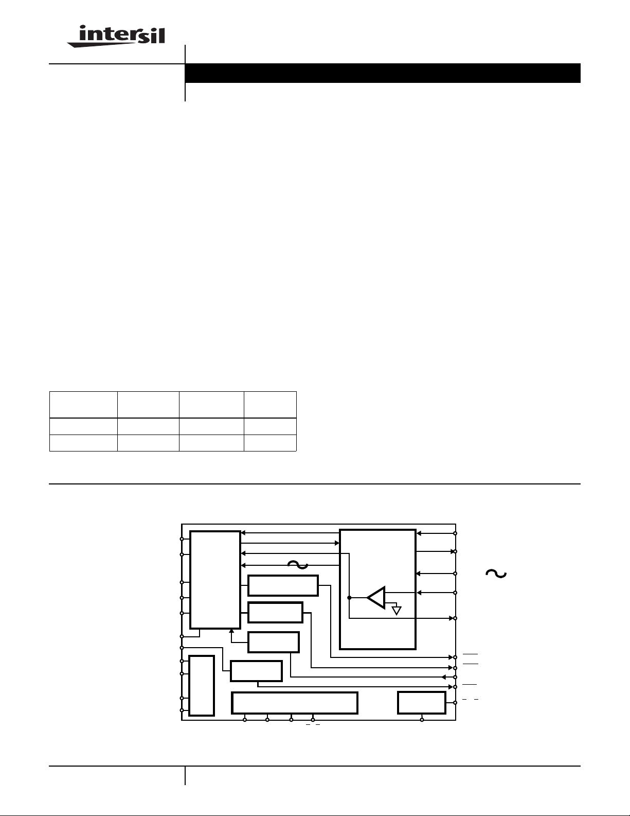
Block Diagram
TIP FEED
TIP SENSE
RING FEED
RING SENSE 1
RING SENSE 2
V
REF
RTI
V
BAT
V
CC
AGND
BGND
2-WIRE
INTERFACE
BIAS
LOOP CURRENT
DETECTOR
CURRENT
RING TRIP
DETECTOR
IIL LOGIC INTERFACE
DETECTOR
FAULT
LIMIT
• Solid State Line Interface Circuit for Hybrid Fiber Coax, Set
Top Box, Voice/Data Modems
• Related Literature
- AN9607, Impedance Matching Design Equations
- AN9628, AC Voltage Gain
- AN9636, Implementing an Analog Port for ISDN
- AN549, The HC-5502/4X Telephone SLIC
V
4-WIRE
INTERFACE
-
+
RELAY
DRIVER
RX
V
TX
V
RING
- IN 1
OUT 1
SHD
ALM
I
LIMIT
RTD
RDO
61
F1 F0 RS
CAUTION: These devices are sensitive to electrostatic discharge; follow proper IC Handling Procedures.
TST RDI
http://www.intersil.com or 407-727-9207 | Copyright © Intersil Corporation 1999

HC5517B
Absolute Maximum Ratings T
Maximum Supply Voltages
(VCC) . . . . . . . . . . . . . . . . . . . . . . . . . . . . . . . . . . . . .-0.5V to +7V
(VCC)-(V
Relay Drivers . . . . . . . . . . . . . . . . . . . . . . . . . . . . . . . .-0.5V to +15V
) . . . . . . . . . . . . . . . . . . . . . . . . . . . . . . . . . . . . . .90V
BAT
Operating Conditions
Temperature Range
HC5517BCM, HC5517BCB . . . . . . . . . . . . . . . . . . . .0oC to 75oC
Relay Drivers . . . . . . . . . . . . . . . . . . . . . . . . . . . . . . . . .+5V to +12V
Positive Power Supply (VCC). . . . . . . . . . . . . . . . . . . . . . . +5V ±5%
Negative Power Supply (V
CAUTION: Stresses above those listed in “Absolute Maximum Ratings” may cause permanent damage to the device. This is a stress only rating and operationofthe
device at these or any other conditions above those indicated in the operational sections of this specification is not implied
NOTES:
1. θJAis measured with the component mounted on an evaluation board PC board in free air.
2. All grounds (AGND, BGND) must be applied before VCCor V
to run separate grounds off a line card, the AGND must be applied first.
) . . . . . . . . . . . . . . . . . . .-16V to -80V
BAT
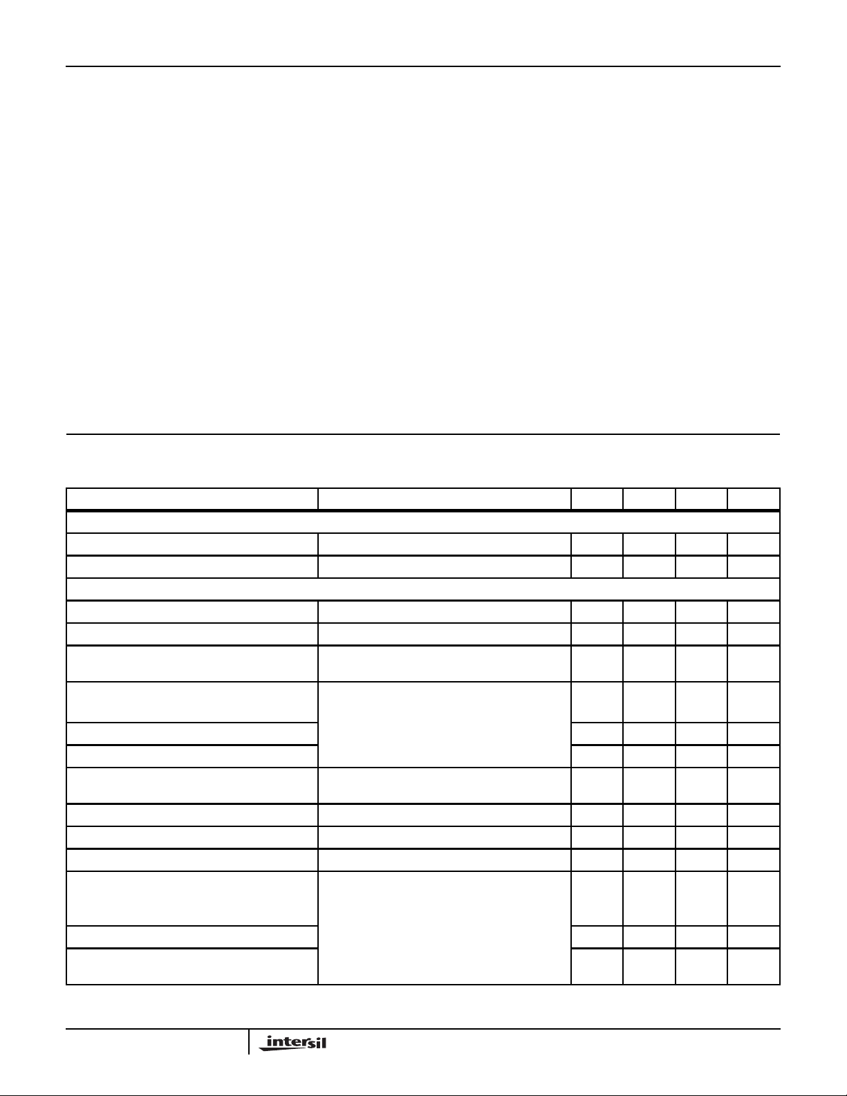
Electrical Specifications Unless Otherwise Specified, Typical Parameters are at T
PARAMETER TEST CONDITIONS MIN TYP MAX UNITS
RINGING TRANSMISSION PARAMETERS
Input Impedance (Note 3) 5.4 kΩ
V
RING
4-Wire to 2-Wire Gain V
AC TRANSMISSION PARAMETERS
RX Input Impedance 300Hz to 3.4kHz (Note 3) 108 kΩ
TX Output Impedance 300Hz to 3.4kHz (Note 3) 20 Ω
4-Wire Input Overload Level 300Hz to 3.4kHz R
2-Wire Return Loss Matched for 600Ω (Note 3)
SRL LO 26 35 dB
ERL 30 40 dB
SRL HI 30 40 dB
2-Wire Longitudinal to Metallic Balance
Off Hook
4-Wire Longitudinal Balance Off Hook 300Hz to 3400Hz (Note 3) 40 dB
Low Frequency Longitudinal Balance I
Longitudinal Current Capability I
Insertion Loss 0dBm at 1kHz, Referenced 600Ω
2-Wire/4-Wire (Includes External Transhybrid
Amplifier with a Gain of 2.4)
4-Wire/2-Wire ±0.05 ±0.2 dB
4-Wire/4-Wire (Includes External Transhybrid
Amplifier with a Gain of 2.4)
=25oC Thermal Information
A
Thermal Resistance (Typical, Note 1) θJA(oC/W)
PLCC Package. . . . . . . . . . . . . . . . . . . . . . . . . . . . . 55
SOIC Package . . . . . . . . . . . . . . . . . . . . . . . . . . . . . 70
Maximum Junction Temperature, Plastic Packages. . . . . . . . .150oC
Maximum Storage Temperature Range. . . . . . . . . . -65oC to 150oC
Maximum Lead Temperature (Soldering 10s) . . . . . . . . . . . . .300oC
(SOIC, PLCC - Lead Tips Only)
Die Characteristics
Transistor Count. . . . . . . . . . . . . . . . . . . . . . . . . . . . . . . . . . . . . .224
Diode Count. . . . . . . . . . . . . . . . . . . . . . . . . . . . . . . . . . . . . . . . . .28
Die Dimensions . . . . . . . . . . . . . . . . . . . . . . . . . . . . . . . . . 174 x 120
Substrate Potential. . . . . . . . . . . . . . . . . . . . . . . . . . . . . . . . . . .V
Process . . . . . . . . . . . . . . . . . . . . . . . . . . . . . . . . . . . . . . .Bipolar-DI
ESD (Human Body Model) . . . . . . . . . . . . . . . . . . . . . . . . . . . .500V
. Failure to do so may result in premature failure of the part. If a user wishes
BAT
Operating TemperatureRange, V
at 600Ω 2-Wire Terminating Impedance
to Vt-r (Note 3) 40 V/V
RING
(Note 3)
Per ANSI/IEEE STD 455-1976 (Note 3) 300Hz to
3400Hz
= 40mA TA = 25oC (Note 3) 10 23 dBrnc
LINE
= 40mA TA = 25oC (Note 3) 40 mA
LINE
= -24V,VCC= +5V,AGND = BGND = 0V.All AC Parameters are specified
BAT
= 1200Ω, 600Ω Reference
L
= 25oC, Min-Max Parameters are over
A
+1.0 V
40 dB
±0.05 ±0.2 dB
BAT
PEAK
RMS
±0.35 dB
62

HC5517B
Electrical Specifications Unless Otherwise Specified, Typical Parameters are at T
Operating TemperatureRange, V
= -24V,VCC= +5V,AGND = BGND = 0V.All AC Parameters are specified
BAT
= 25oC, Min-Max Parameters are over
A
at 600Ω 2-Wire Terminating Impedance (Continued)
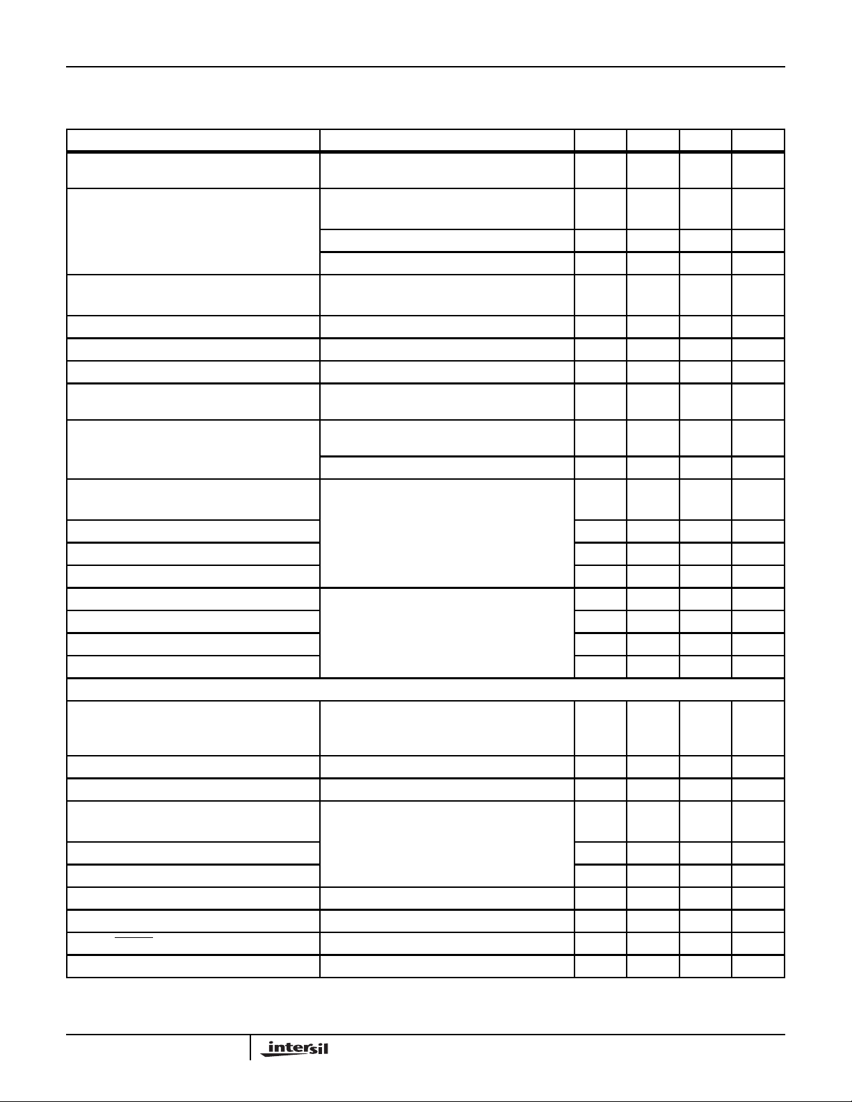
PARAMETER TEST CONDITIONS MIN TYP MAX UNITS
Frequency Response 300Hz to 3400Hz (Note 3) Referenced to Absolute
- ±0.02 ±0.06 dB
Level at 1kHz, 0dBm Referenced 600Ω
Level Linearity Referenced to -10dBm (Note 3)
2-Wire to 4-Wire and 4-Wire to 2-Wire +3 to -40dBm - - ±0.08 dB
-40 to -50dBm - - ±0.12 dB
-50 to -55dBm - - ±0.3 dB
Absolute Delay (Note 3)
2-Wire/4-Wire 300Hz to 3400Hz - - 1.0 µs
4-Wire/2-Wire 300Hz to 3400Hz - - 1.0 µs
4-Wire/4-Wire 300Hz to 3400Hz - 0.95 1.5 µs
Transhybrid Loss V
Total Harmonic Distortion
2-Wire/4-Wire, 4-Wire/2-Wire, 4-Wire/4-Wire
Idle Channel Noise
2-Wire and 4-Wire
= 1V
IN
Reference Level 0dBm at 600Ω
300Hz to 3400Hz (Note 3)
(Note 3)
C-Message
at 1kHz (Note 3,4) 30 40 - dB
P-P
- - -50 dB
- 3 - dBrnC
Psophometric (Note 3) - -87 - dBmp
Power Supply Rejection Ratio (Note 3)
to 2-Wire 20 40 - dB
V
CC
V
to 4-Wire 20 40 - dB
CC
to 2-Wire 20 40 - dB
V
BAT
to 4-Wire 20 50 - dB
V
BAT
V
to 2-Wire (Note 3)
CC
to 4-Wire 20 28 - dB
V
CC
to 2-Wire 20 50 - dB
V
BAT
V
to 4-Wire 20 50 - dB
BAT
30Hz to 200Hz, RL = 600Ω
30 40 - dB
200Hz to 16kHz, RL = 600Ω
DC PARAMETERS
Loop Current Programming
Limit Range 20(Note
-60mA
5)
Accuracy 15 - - %
Loop Current During Power Denial R
= 200Ω - ±4 ±7mA
L
Fault Currents
TIP to Ground (Note 3) -30-mA
RING to Ground - 120 - mA
TIP and RING to Ground (Note 3) - 150 - mA
Switch Hook Detection Threshold -1215mA
Ring Trip Comparator Voltage Threshold -0.28 -0.24 -0.22 V
Thermal
ALARM Output (Note 3) Safe Operating Die Temperature Exceeded 140 - 160
o
C
Dial Pulse Distortion (Note 3) - 0.1 0.5 ms
63

HC5517B
Electrical Specifications Unless Otherwise Specified, Typical Parameters are at T
Operating TemperatureRange, V
= -24V,VCC= +5V,AGND = BGND = 0V.All AC Parameters are specified
BAT
= 25oC, Min-Max Parameters are over
A
at 600Ω 2-Wire Terminating Impedance (Continued)
PARAMETER TEST CONDITIONS MIN TYP MAX UNITS
Uncommitted Relay Driver
On Voltage V
OL
IOL (RDO) = 30mA - 0.2 0.5 V
Off Leakage Current - ±10 ±100 µA
TTL/CMOS Logic Inputs (F0, F1, RS, TST, RDI)
Logic ‘0’ V
Logic ‘1’ V
IL
IH
Input Current (F0, F1, RS,
Input Current (F0, F1, RS,
TST, RDI) IIH, 0V ≤ VIN≤ 5V - - -1 µA
TST, RDI) IIL, 0V ≤ VIN≤ 5V - - -100 µA
0 - 0.8 V
2.0 - 5.5 V
Logic Outputs
Logic ‘0’ V
Logic ‘1’ V
OL
OH
Power Dissipation On Hook V
Power Dissipation Off Hook V
I
= 800µA - 0.3 0.6 V
LOAD
I
= 40µA 2.7 - - V
LOAD
CC
V
CC
CC
= +5V, V
= +5V, V
= +5V, V
= -80V, R
BAT
= -48V, R
BAT
= -24V, R
BAT
= ∞ - 300 - mW
LOOP
= ∞ - 150 - mW
LOOP
LOOP
= 600Ω,
- 280 - mW
IL = 25mA
I
CC
I
BAT
VCC = +5V, V
= +5V, V
V
CC
V
= +5V, V
CC
VCC = +5V, VB- = -80V, R
= +5V, VB- = -48V, R
V
CC
V
= +5V, VB- = -24V, R
CC
= -80V, R
BAT
= -48V, R
BAT
= -24V, R
BAT
= ∞ -36mA
LOOP
= ∞ -25mA
LOOP
= ∞ - 1.9 4 mA
LOOP
= ∞ - 3.6 7 mA
LOOP
= ∞ - 2.6 6 mA
LOOP
= ∞ - 1.8 4 mA
LOOP
UNCOMMITTED OP AMP PARAMETERS
Input Offset Voltage - ±5-mV
Input Offset Current - ±10 - nA
Differential Input Resistance (Note 3) - 1 - MΩ
Output Voltage Swing (Note 3) R
= 10kΩ - ±3-V
L
P-P
Small Signal GBW (Note 3) - 1 - MHz
NOTES:
3. These parameters are controlled by design or process parameters and are not directly tested. These parameters are characterized upon initial
design release, upon design changes which would affect these characteristics, and at intervals to assure product quality and specification compliance.
4. For transhybrid circuit as shown in Figure 3.
5. Application limitation based on maximum switch hook detect limit and metallic currents. Not a part limitation.
64
