HC55171
Data Sheet July 1998 File Number
5 REN Ringing SLIC for
ISDN Modem/TA and WLL
The HC55171 is backward compatible to the HC5517 with
the added capability of driving 5 REN loads. The HC55171 is
ideal for any modem or remote networking access
application that requires plain old telephone service POTS,
capability. The linear amplifier design allows a choice of
Sinusoidal, Square wave or Trapezoidal ringing. The voltage
feed architecture eliminates the need for a high current gain
node achieving improved system noise immunity, an
advantage in highly integrated systems.
The device is manufactured in a high voltage Dielectric
Isolation (DI) process with an operating voltage range from
-16V,foroff-hookoperation and -80V for ring signal injection.
The DI process provides substrate latch up immunity,
resulting in a robust system design.
Ordering Information
TEMP. RANGE
PART NUMBER
HC55171IM -40 to 85 28 Ld PLCC N28.45
HC55171CM 0 to 75 28 Ld PLCC N28.45
HC55171IB -40 to 85 28 Ld SOIC M28.3
HC55171CB 0 to 75 28 Ld SOIC M28.3
(oC) PACKAGE
PKG.
NO.
4323.4
Features
• 5 REN Thru SLIC Ringing Capability to 75V
• Trapezoid, Square and Sinusoid Ringing Capability
• Bellcore Compliant Ringing Voltage Levels
• Lowest Component Count Trapezoidal Solution
• Single Additional +5V Supply
• Pin For Pin Compatible With HC5517
• DI Provides Latch-Up Immunity
PEAK
Applications
• ISDN Internal/External Modems
• ISDN Terminal Adapters/Routers
• Wireless Local Loop Subscriber Terminals
• Cable Telephony Set-Top Boxes
• Digital Added Main Line
• Integrated LAN/PBX
• Related Literature
- AN9606, Operation of the HC5517/171 Evaluation
Board
- AN9607, Impedance Matching Design Equations
- AN9628, AC Voltage Gain
- AN9608, Implementing Pulse Metering
- AN9636, Implementing an Analog Port for ISDN Using
the HC5517
- AN549, The HC-5502X/4X Telephone Subscriber Line
Interface Circuits (SLIC)
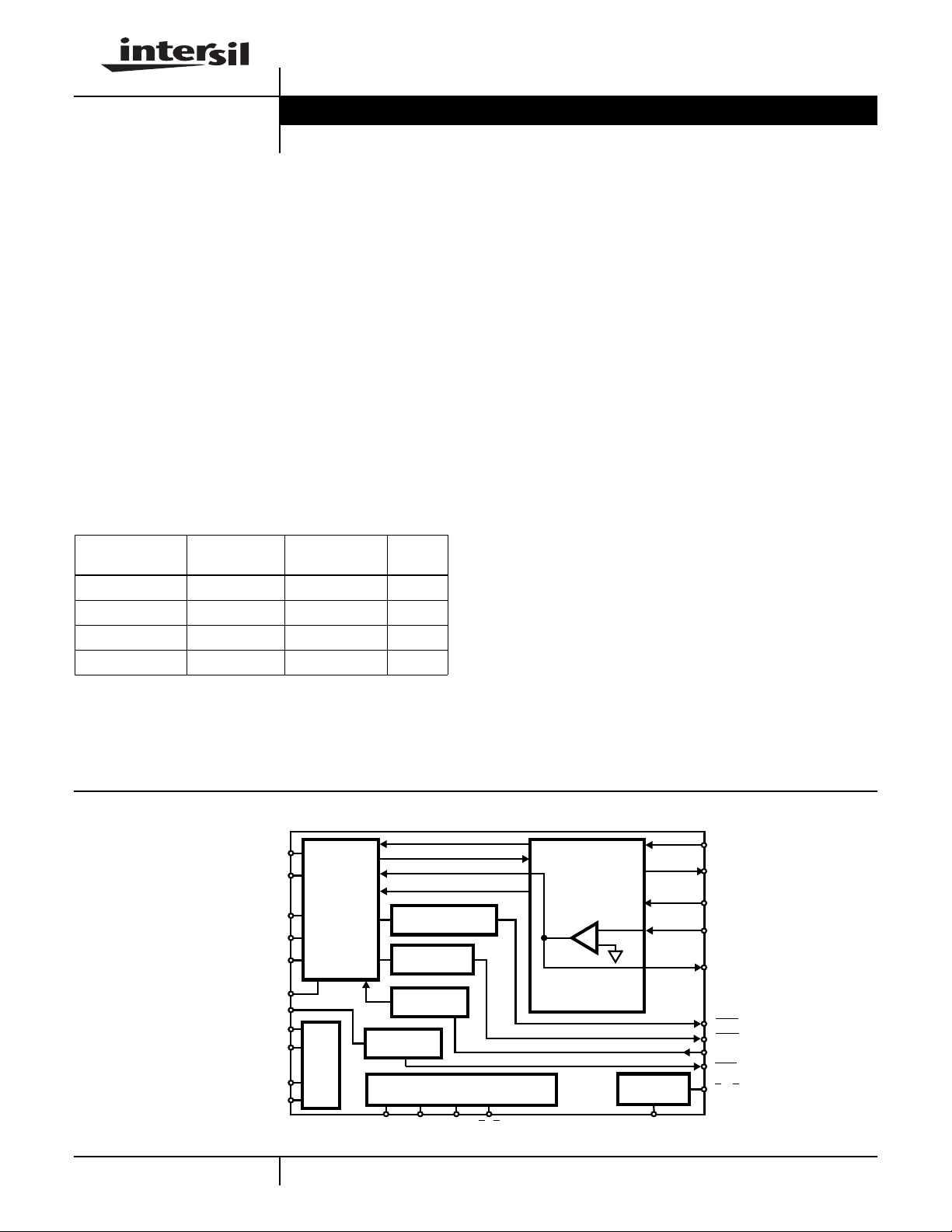
Block Diagram
TIP FEED
TIP SENSE
RING FEED
RING SENSE 1
RING SENSE 2
V
REF
RTI
V
BAT
V
CC
AGND
BGND
62
2-WIRE
INTERFACE
BIAS
V
4-WIRE
INTERFACE
LOOP CURRENT
DETECTOR
FAULT
DETECTOR
CURRENT
LIMIT
RING TRIP
DETECTOR
IIL LOGIC INTERFACE
F1 F0 RS
CAUTION: These devices are sensitive to electrostatic discharge; follow proper IC Handling Procedures.
TST RDI
http://www.intersil.com or 407-727-9207 | Copyright © Intersil Corporation 1999
-
+
RELAY
DRIVER
RX
V
TX
V
RING
- IN 1
OUT 1
SHD
ALM
I
LMT
RTD
RDO
HC55171
Absolute Maximum Ratings T
Maximum Supply Voltages
VCC . . . . . . . . . . . . . . . . . . . . . . . . . . . . . . . . . . . . . .-0.5V to +7V
VCC- V
Relay Drivers . . . . . . . . . . . . . . . . . . . . . . . . . . . . . . . .-0.5V to +15V
. . . . . . . . . . . . . . . . . . . . . . . . . . . . . . . . . . . . . . . .90V
BAT
Operating Conditions
Temperature Range
HC55171IM, HC55171IB . . . . . . . . . . . . . . . . . . . . -40oC to 85oC
HC55171CM, HC55171CB . . . . . . . . . . . . . . . . . . . .0oC to 75oC
Relay Drivers . . . . . . . . . . . . . . . . . . . . . . . . . . . . . . . . .+5V to +12V
Positive Power Supply, VCC. . . . . . . . . . . . . . . . . . . . . . . . +5V ±5%
Negative Power Supply, V
CAUTION: Stresses above those listed in “Absolute Maximum Ratings” may cause permanent damage to the device. This is a stress only rating and operationofthe
device at these or any other conditions above those indicated in the operational sections of this specification is not implied
NOTE:
1. θJA is measured with the component mounted on an evaluation PC board in free air.
. . . . . . . . . . . . . . . . . . . .-16V to -80V
BAT
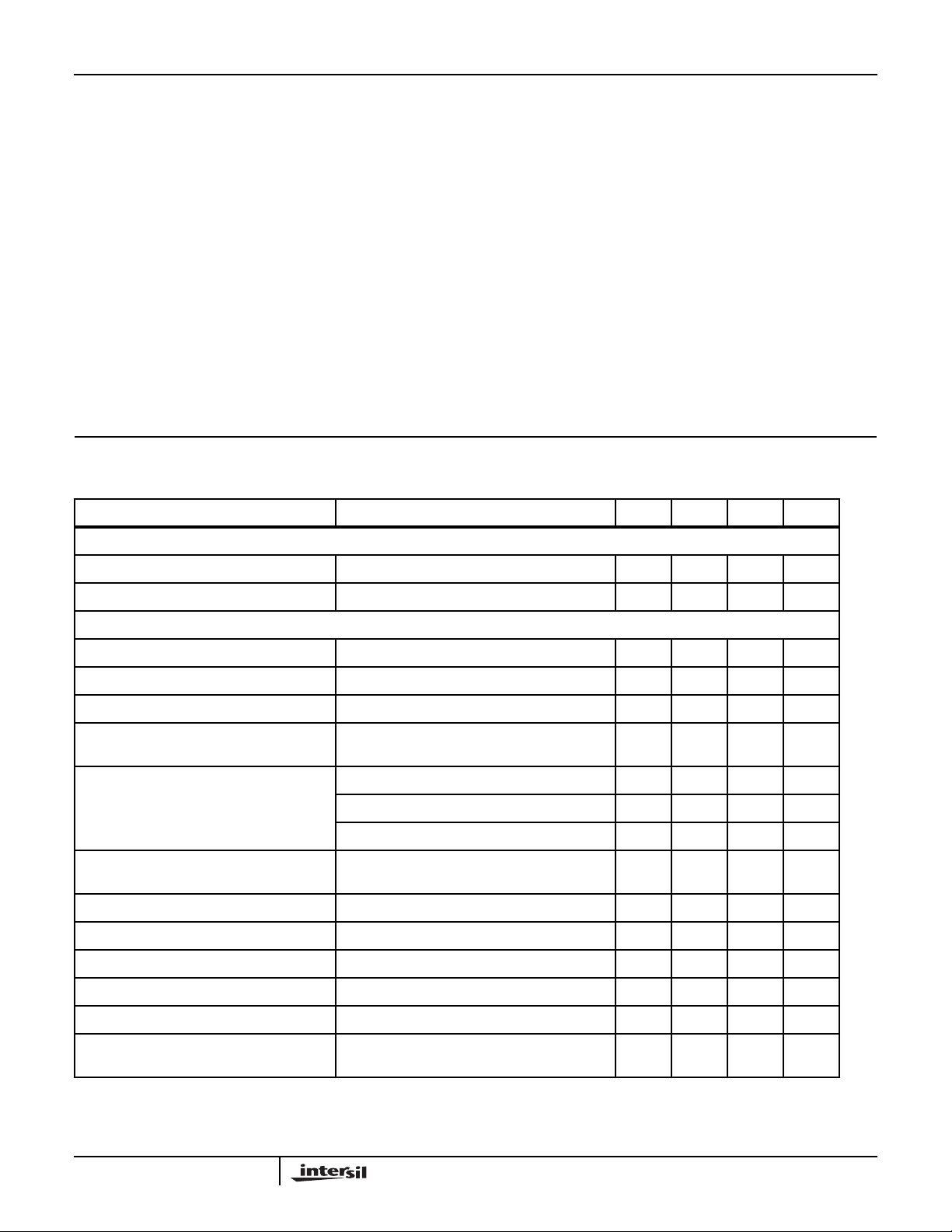
Electrical Specifications Unless Otherwise Specified, Typical Parameters are at T
PARAMETER TEST CONDITIONS MIN TYP MAX UNITS
RINGING TRANSMISSION PARAMETERS
=25oC Thermal Information
A
Thermal Resistance (Typical, Note 1) θJA(oC/W)
PLCC . . . . . . . . . . . . . . . . . . . . . . . . . . . . . . . . . . . . 55
SOIC . . . . . . . . . . . . . . . . . . . . . . . . . . . . . . . . . . . . 70
Maximum Junction Temperature Plastic . . . . . . . . . . . . . . . . .150oC
Maximum Storage Temperature Range. . . . . . . . . . -65oC to 150oC
Maximum Lead Temperature (Soldering 10s) . . . . . . . . . . . . .300oC
(SOIC, PLCC - Lead Tips Only)
Die Characteristics
Transistor Count. . . . . . . . . . . . . . . . . . . . . . . . . . . . . . . . . . . . . .224
Diode Count. . . . . . . . . . . . . . . . . . . . . . . . . . . . . . . . . . . . . . . . . .28
Die Dimensions . . . . . . . . . . . . . . . . . . . . . . . . . . . . . . . . . 175 x 144
Substrate Potential. . . . . . . . . . . . . . . . . . . . . . . . . . . . . . . . . . .V
Process . . . . . . . . . . . . . . . . . . . . . . . . . . . . . . . . . . . . . . .Bipolar-DI
Operating TemperatureRange, V
at 600Ω 2-Wire terminating impedance.
= -24V,VCC= +5V,AGND = BGND = 0V.All AC Parametersare specified
BAT
= 25oC, Min-Max Parameters are over
A
BAT
V
Input Impedance (Note 2) - 5.4 - kΩ
RING
4-Wire to 2-Wire Gain V
AC TRANSMISSION PARAMETERS
RX Input Impedance 300Hz to 3.4kHz (Note 2) - 108 - kΩ
OUT1 Positive Output Voltage Swing RL = 10kΩ (Note 2) +2.5 - - V
OUT1 Negative Output Voltage Swing RL = 10kΩ (Note 2) -4.5 - - V
4-Wire Input Overload Level 300Hz to 3.4kHz RL = 1200Ω, 600Ω Reference
2-Wire Return Loss Matched for 600Ω, f = 300Hz (Note 2) 37 - - dB
2-Wire Longitudinal to Metallic Balance
Off Hook
4-Wire Longitudinal Balance Off Hook 300Hz to 3400Hz (Note 2) - 55 - dB
Longitudinal Current Capability I
Insertion Loss, 2W-4W 0dBmO, 1kHz, Includes Tranhybrid Amp Gain = 3 - ±0.05 ±0.2 dB
Insertion Loss, 4W-2W 0dBmO,1kHz - ±0.05 ±0.2 dB
Insertion Loss, 4W-4W 0dBmO, 1kHz, Includes Tranhybrid Amp Gain = 3 - - ±0.25 dB
to V
RING
(Note 2)
Matched for 600Ω, f = 1000Hz (Note 2) 40 - - dB
Matched for 600Ω, f = 3400Hz (Note 2) 30 - - dB
Per ANSI/IEEE STD 455-1976 300Hz to 3400Hz
(Note 2)
= 40mA, TA = 25oC (Note 2) - 40 - mA
LINE
(Note 2) - 40 - V/V
T-R
- +3.1 - V
58 63 - dB
PEAK
RMS
Frequency Response 300Hz to 3400Hz Referenced to Absolute Level
at 1kHz, 0dBm Referenced 600Ω
63
- ±0.02 ±0.06 dB
HC55171
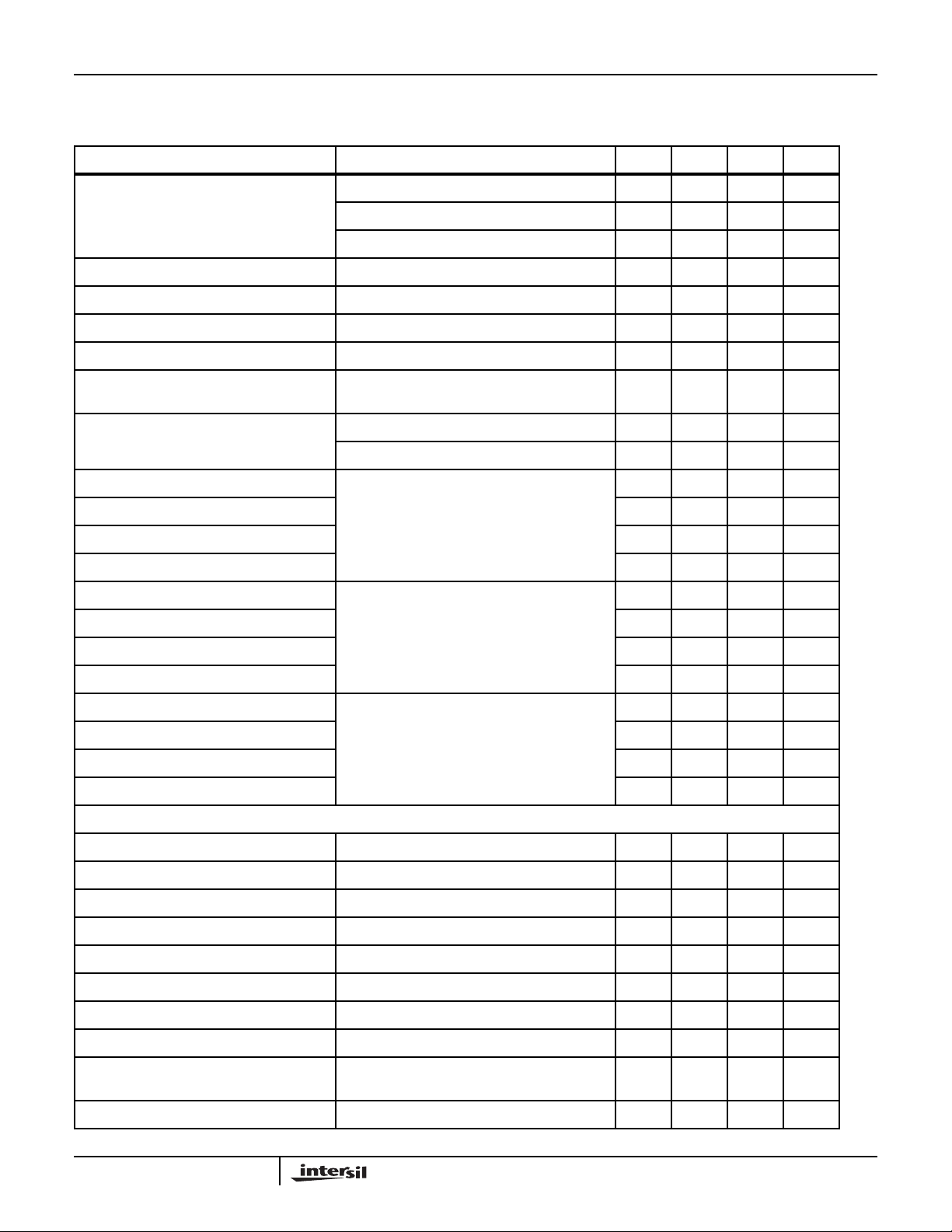
Electrical Specifications Unless Otherwise Specified, Typical Parameters are at T
Operating TemperatureRange, V
at 600Ω 2-Wire terminating impedance. (Continued)
PARAMETER TEST CONDITIONS MIN TYP MAX UNITS
Level Linearity +3 to 0dBm, Referenced to -10dBm (Note 2) - - ±0.10 dB
0 to -40dBm, Referenced to -10dBm (Note 2) - - ±0.12 dB
-40 to -55dBm, Referenced to -10dBm (Note 2) - - ±0.30 dB
Absolute Delay, 2W-4W 300Hz to 3400Hz (Note 2) - - 1.0 µs
Absolute Delay, 4W-2W 300Hz to 3400Hz (Note 2) - - 1.0 µs
Absolute Delay, 4W-4W 300Hz to 3400Hz (Note 2) - 0.95 - µs
Transhybrid Loss VIN = 1V
Total Harmonic Distortion
2-Wire/4-Wire, 4-Wire/2-Wire, 4-Wire/4-Wire
Idle Channel Noise
2-Wire and 4-Wire
PSRR, VCC to 2W 30Hz to 200Hz, RL = 600Ω (Note 2) 30 35 - dB
PSRR, VCC to 4W 45 47 - dB
PSRR, VBAT to 2W 23 28 - dB
Reference Level 0dBm at 600Ω
300Hz to 3400Hz (Note 2)
C-Message (Note 2) - 3 - dBrnC
Psophometric (Note 2) - -87 - dBmp
at 1kH (Note 2) 36 40 - dB
P-P
= -24V,VCC= +5V,AGND = BGND = 0V.All AC Parametersare specified
BAT
= 25oC, Min-Max Parameters are over
A
- - -50 dB
PSRR, VBAT to 4W 33 38 - dB
PSRR, VCC to 2W 200Hz to 3.4kHz, RL = 600Ω (Note 2) 33 35 - dB
PSRR, VCC to 4W 44 46 - dB
PSRR, VBAT to 2W 40 50 - dB
PSRR, VBAT to 4W 50 60 - dB
PSRR, VCC to 2W 3.4kHz to 16kHz, RL = 600Ω (Note 2) 30 34 - dB
PSRR, VCC to 4W 35 40 - dB
PSRR, VBAT to 2W 30 40 - dB
PSRR, VBAT to 4W 40 50 - dB
DC PARAMETERS
Loop Current Programming Range (Note 3) 20 - 60 mA
Loop Current Programming Accuracy -10 - +10 %
Loop Current During Power Denial RL = 200Ω, V
Fault Current, Tip to Ground (Note 2) - 90 - mA
Fault Current, Ring to Ground - 100 - mA
Fault Current, Tip and Ring to Ground (Note 2) - 130 - mA
Switch Hook Detection Threshold 9 12 15 mA
= -48V - ±4-mA
BAT
Ring Trip Comparator Voltage Threshold -0.28 -0.24 -0.22 V
Thermal ALARM Output Safe Operating Die Temperature Exceeded
(Note 2)
Dial Pulse Distortion (Note 2) - 0.1 0.5 ms
- 160 -
o
64
C
HC55171
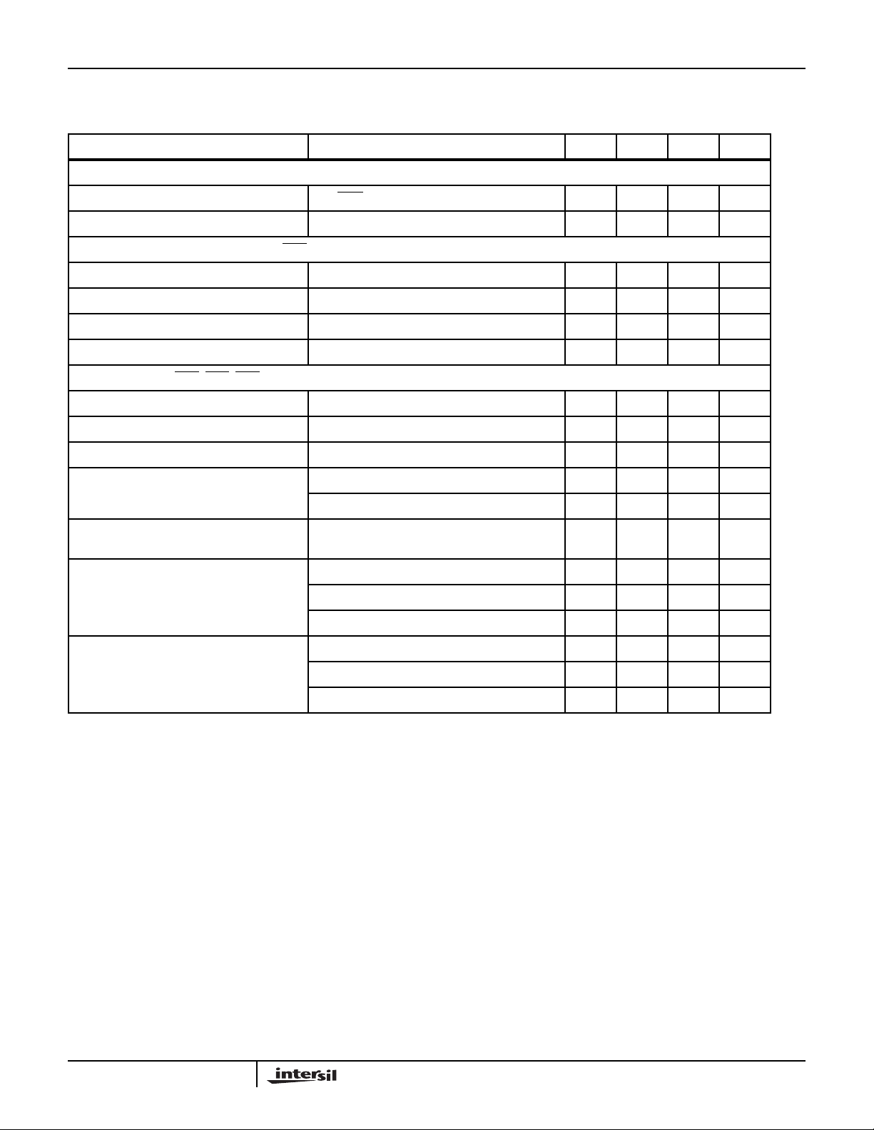
Electrical Specifications Unless Otherwise Specified, Typical Parameters are at T
Operating TemperatureRange, V
= -24V,VCC= +5V,AGND = BGND = 0V.All AC Parametersare specified
BAT
= 25oC, Min-Max Parameters are over
A
at 600Ω 2-Wire terminating impedance. (Continued)
PARAMETER TEST CONDITIONS MIN TYP MAX UNITS
UNCOMMITTED RELAY DRIVER
On Voltage, V
OL
IOL (RDO) = 30mA - 0.2 0.5 V
Off Leakage Current - ±10 ±100 µA
TTL/CMOS LOGIC INPUTS (F0, F1, RS, TST, RDI)
Logic Low Input Voltage 0 - 0.8 V
Logic High Input Voltage 2.0 - 5.5 V
Input Current IIH, 0V ≤ VIN≤ 5V - - -1 µA
Input Current IIL, 0V ≤ VIN≤ 5V - - -100 µA
LOGIC OUTPUTS (SHD, RTD, ALM)
Logic Low Output Voltage I
Logic High Output Voltage I
= 800µA - 0.1 0.5 V
LOAD
= 40µA 2.7 - 5.5 V
LOAD
POWER DISSIPATION --Power Dissipation On Hook VCC = +5V, V
VCC = +5V, V
Power Dissipation Off Hook VCC = +5V, V
= -80V, R
BAT
= -48V, R
BAT
= -24V, R
BAT
= ∞ - 300 - mW
LOOP
= ∞ - 150 - mW
LOOP
LOOP
= 600Ω,
- 280 - mW
IL = 25mA
I
CC
I
BAT
VCC = +5V, V
VCC = +5V, V
VCC = +5V, V
= -80V, R
BAT
= -48V, R
BAT
= -24V, R
BAT
VCC = +5V, VB- = -80V, R
VCC = +5V, VB- = -48V, R
VCC = +5V, VB- = -24V, R
= ∞ -36mA
LOOP
= ∞ -25mA
LOOP
= ∞ - 1.9 5 mA
LOOP
= ∞ - 3.6 7 mA
LOOP
= ∞ - 2.6 6 mA
LOOP
= ∞ - 2.3 4.5 mA
LOOP
NOTES:
2. These parameters arecontrolledby design or processparameters and are notdirectlytested. These parameters arecharacterized upon
initial design release, upon design changes which would affect these characteristics, and at intervals to assure product quality and
specification compliance.
3. This parameter directly affects device junction temperature. Refer to Power Dissipation discussion of data sheet for design information.
65
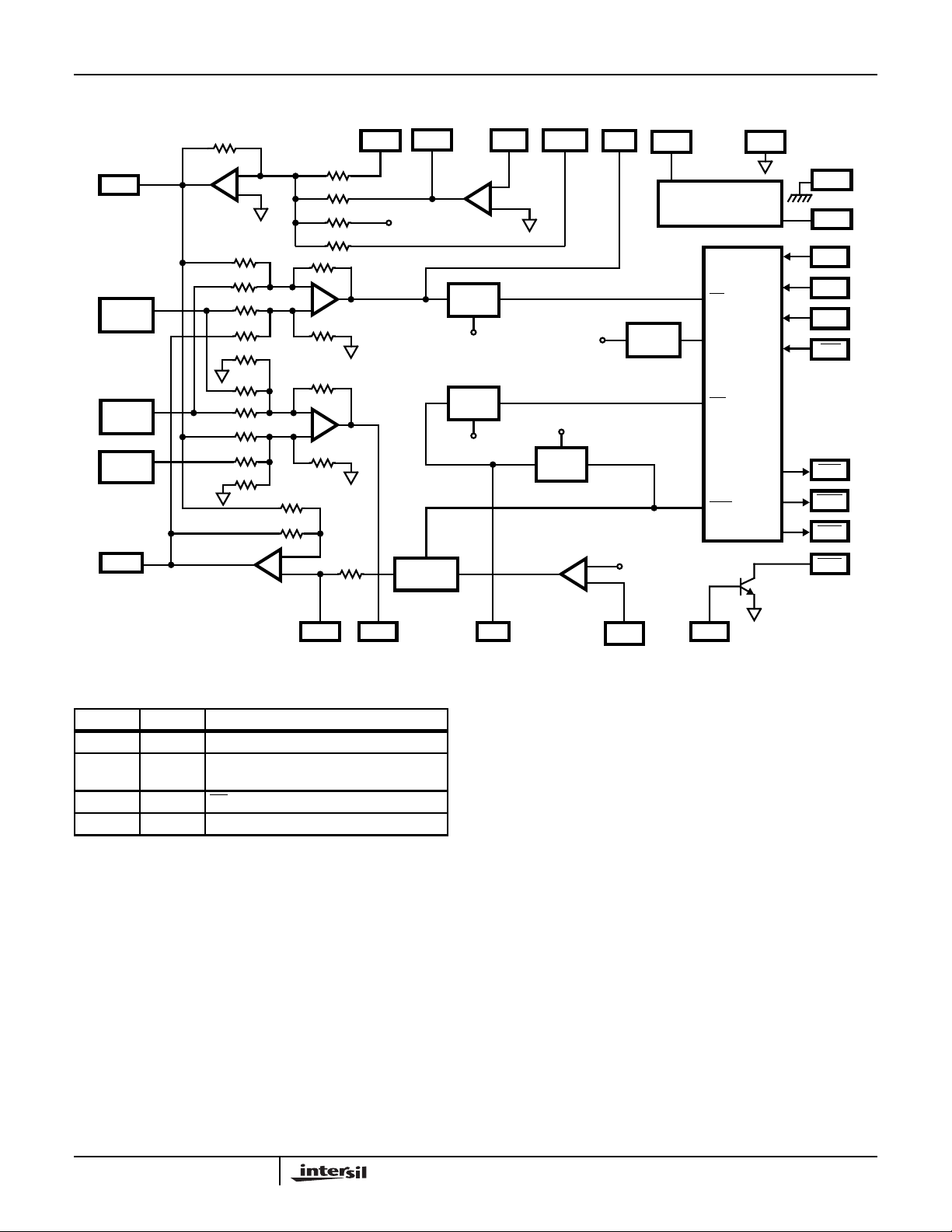
Functional Diagram
HC55171
TF
TIP
SENSE
RING
SENSE 1
RING
SENSE 2
RF
R
2R
-
+
2R
25K
-
+
25K
R
R
R/2
R/20
TA
RA
90K
TF
25
14
15
16
26
-
+
4.5K
100K
100K
100K
100K
4.5K
R
R
R
R
90K
90K
RF
-
+
V
RX
17 12
+2V
OUT 1
VB/2
REF
SHD
RTD
-
+
-IN 1
OP AMP
V
RING
13 24 19 2
FAULT
DET
GM
V
-
+
TX
THERM
LTD
RF2
V
CC
BIAS
NETWORK
SH
TSD
GK
RFC
AGND
IIL LOGIC INTERFACE
1
22
BGND
27
V
BAT
4
F1
5
F0
6
RS
9
TST
7
SHD
8
RTD
10
ALM
21
RDO
R = 108kΩ
3
V
REF
18
HC55171 DEVICE TRUTH TABLE
F1 F0 STATE
0 0 Loop power Denial Active
0 1 Power Down Latch RESET, Power on
RESET
10
RD Active
1 1 Normal Loop feed
The truth table for the internal logic of the HC55171 is provided in the above table. This family of ringing SLICS can be
configured to support traditional unbalanced ringing and thru
SLIC balanced ringing. Refer to the HC5509A1R3060 for
unbalanced ringing application information. The device operating states used by thru SLIC ringing applications are loop
power denial and normal feed. During loop power denial, the
tip and ring amplifiers are disabled (high impedance) and the
DC voltage of each amplifier approaches ground. The SLIC
will not provide current to the subscriber loop during this mode
and will not detect loop closure. Voice transmission occurs
during the normal loop feed mode. During normal loop feed
the SLIC is completely operational and performs all transmission and supervisory functions.
28
RTINU I
11
LMT
20
RDI
Power Dissipation
Careful thermal design is required to guarantee that the
maximum junction temperature of 150
o
C of the device is not
exceeded. The junction temperature of the SLIC can be calculated using:
TJTAθJAICCVCCI
BATVBATILOOP
()2R
•()–+()+=
LOOP
Where TAis maximum ambient temperature and θJAis junction to air thermal resistance (and is package dependent).
The entire term in parentheses yields the SLIC power dissipation. The power dissipation of the subscriber loop does
not contribute to device junction temperature and is subtracted from the power dissipation term. Operating at 85
the maximum PLCC SLIC power dissipation is 1.18W. Likewise, the maximum SOIC SLIC power dissipation is 0.92W.
(EQ. 1)
o
C,
66
HC55171
Circuit Operation and Design Information
Introduction
The HC55171 is a high voltage Subscriber Line Interface Circuit (SLIC) specifically designed for through SLIC ringing
applications. Through SLIC ringing applications are broadly
defined as any application that requires ringing capability but
does not have the standard wired central office interface. The
most common implementation of the ringing SLIC is in the
analog pots port. The analog pots port provides the ringing
function as well as interface compatibility with answering and
fax machines.
Subscriber Line Interface Basics
The basic SLIC provides DC loop current to power the handset,
supports full duplex analog transmission between the handset
and CODEC, matches the impedance of the SLIC to the
impedance of the handset and performs loop supervision functions to detect when the handset is off hook.
adds through the SLIC ringing capability to this suite of features.
The analog interfaces of the SLIC are categorized as the
2-wire interface(high voltageDC,differential AC) and the 4-wire
interface (low voltage DC, single ended AC).
DC Loop Current
The Tip and Ring terminals of the subscriber line circuit are
biased at negative potentials with respect to ground. The Tip
terminal DC potential is slightly negative with respect to
ground, and the ring terminal DC potential is slightly positive
with respect to the battery voltage (resulting in a large negative voltage). The HC55171 typical Tip DC voltage is -4V and
the typical ring DC voltage is defined as V
ple, when the battery voltage is -24V the ring voltage is -20V.
To clearly comprehend the Tip and Ring interface it is helpful
to understand that the handset and the SLIC constitute a DC
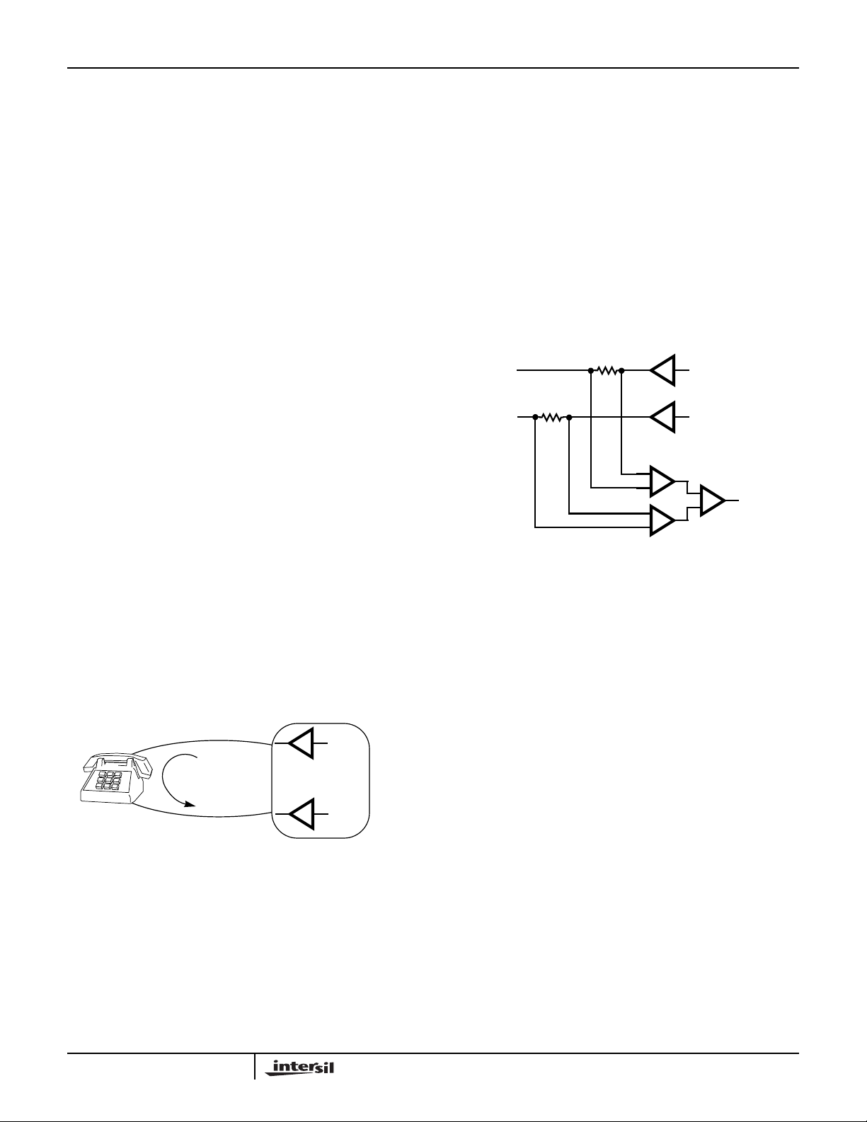
and AC current loop as shown in Figure 1. The loop is often
referred to as the subscriber loop.
LOOP
CURRENT
FIGURE 1. SUBSCRIBER LOOP
When the handset is on hook (idle) the phone is an open circuit load and the DC loop current is zero. The SLIC can still
provide AC transmission in this condition, which supports
caller id services. The DC resistance of the off hook handset
is typically 400Ω. Since the Tip DC voltage is more positive
than the ring DC voltage, DC loop current flows from Tip to
Ring when the handset is off hook. The SLIC is designed
with feedback to limit the maximum loop current when the
handset is off hook.
The ringing SLIC
+ 4V. For exam-
BAT
TIP
RING
SLIC
Full Duplex Analog Transmission
Familiarity with the signal paths of the SLIC is critical in
understanding the full duplex transmission capability of the
device. The analog interfaces of the SLIC are categorized as
2-wire interfaces and 4-wire interfaces.
The 2-wire interface of the SLIC consists of the bidirectional
Tip and Ring terminals of the device. A differential transmitter drives AC signals out of the Tip and Ring terminals to the
handset. A differential receiver across Tip and Ring receives
AC signals from the handset. The differential receiver is connected across sense resistors that are in the Tip and Ring
signal paths. The differential transmitter and receiver concept is depicted in Figure 2.
DIFFERENTIAL
TRANSMITTER
-1
-
+
-
+
FIGURE 2. DIFFERENTIAL TRANSMIT/RECEIVE CONCEPT
-
+
DIFFERENTIAL
RECEIVER
Since the receiver is connected across the transmit signal
path, one may deduce that in addition to receiving signals
from the handset, the receiver will detect part of the transmit
signal. Indeed this does occur and is the reason that all SLIC
circuits require a hybrid balance or echo cancellation function.
The 4-wire interface of the SLIC consists of the receive
(VRX) and transmit (OUT1) terminals. The 4-wire interfaces
are single ended signal paths. The receiver is a dedicated
input port and the transmitter is a dedicated output port. The
4-wire receive input of the SLIC drives the 2-wire differential
transmitter and the 2-wire differential receiver drives the 4wire transmit output.
The complete signal path for voice signals includes two digital data busses, a CODEC and a SLIC. There is a receive
data bus and transmit data bus, each with an independent 3wire serial interface. The CODEC contains a coder and
decoder. The coder converts the SLIC analog transmit output to digital data for the transmit data bus. The receive digital data bus is converted to analog data and drives the SLIC
receive input.
The CODECs use logarithmic compression schemes to
extend the resolution of the 8-bit data to 14 bits. The
accepted compression schemesareA-law(Intersil CODEC CD22357A) and µ-law (Intersil CODEC - CD22354A). The
complete signal path from the handset to the CODEC is
shown in Figure 3.
67
 Loading...