Intersil Corporation HC5517 Datasheet

HC5517
Data Sheet July 1998 File Number
3 REN Ringing SLIC For ISDN Modem/TA
and WLL
he HC5517 is a ringing SLIC designed to accommodate a wide
variety of local loop applications. The various applications
include, basic POTS lines with ans w ering machines and fax
capabilities, ISDN networks, wireless local loop, and h ybrid
fiber coax (HFC) terminals. The HC5517 provides a high
degreeofflexibilitywith open circuit tip to ring DC voltages,user
defined ringing waveforms(sinusoidal to square wave),ring trip
detection thresholds and loop current limits that can be tailored
for many applications. Additional f eatures of the HC5517 are
complex impedance matching, pulse metering and transhybrid
balance. The HC5517 is designed for use in systems where a
separate ring generator is not economically feasible.
The device is manufacturedin a high voltage Dielectric Isolation
(DI) process with an operating voltage range from -16V, for offhook operation and -80V for ring signal injection. The DI
process provides substrate latch up immunity, resulting in a
robust system design. Together with a secondary protection
diode bridge and “feed” resistors, the device will withstand
1000V lightning induced surges, in a plastic package.
A thermal shutdown with an alarm output and line fault
protection are also included for operation in harsh
environments.
Ordering Information
PART
NUMBER
HC5517IM -40 to 85 28 Ld PLCC N28.45
HC5517CM 0 to 75 28 Ld PLCC N28.45
HC5517IB -40 to 85 28 SOIC M28.3
HC5517CB 0 to 75 28 SOIC M28.3
TEMP.RANGE
(oC) PACKAGE PKG. NO.
4147.2
Features
• Thru-SLIC Open Circuit Ringing Voltage up to
77V
PEAK
/54V
, 3 REN Capability at 44V
RMS
RMS
• Sinusoidal Ringing Capability
• DI Process Provides Substrate Latch Up Immunity when
Driving Inductive Ringers
• Adjustable On-Hook Voltage for Fax and Answering
Machine Compatibility
• Resistive and Complex Impedance Matching
• Programmable Loop Current Limit
• Switch Hook and Adjustable Ring Trip Detection
• Pulse Metering Capability
• Single Low Voltage Positive Supply (+5V)
Applications
• Solid State Line Interface Circuit for Wireless Local Loop,
Hybrid Fiber Coax, Set Top Box, Voice/Data Modems
• Related Literature
- AN9606, Operation of the HC5517 Evaluation Board
- AN9607, Impedance Matching Design Equations
- AN9628, AC Voltage Gain
- AN9608, Implementing Pulse Metering
- AN9636, Implementing an Analog Port for ISDN Using
the HC5517
- AN549, The HC-5502S/4X Telephone Subscriber Line
Interface Circuits (SLIC)
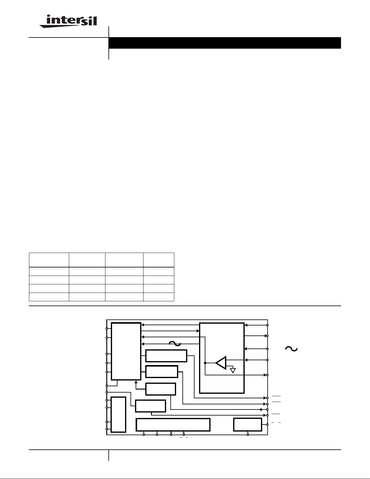
Block Diagram
RING SENSE 1
RING SENSE 2
TIP FEED
TIP SENSE
RING FEED
V
REF
RTI
V
BAT
V
CC
AGND
BGND
60
2-WIRE
INTERFACE
BIAS
V
4-WIRE
INTERFACE
LOOP CURRENT
DETECTOR
FAULT
DETECTOR
CURRENT
LIMIT
RING TRIP
DETECTOR
IIL LOGIC INTERFACE
F1 F0 RS
CAUTION: These devices are sensitive to electrostatic discharge; follow proper IC Handling Procedures.
TST RDI
http://www.intersil.com or 407-727-9207 | Copyright © Intersil Corporation 1999
-
+
RELAY
DRIVER
RX
V
TX
V
RING
- IN 1
OUT 1
SHD
ALM
I
LMT
RTD
RDO

HC5517
Absolute Maximum Ratings T
Maximum Supply Voltages
(VCC) . . . . . . . . . . . . . . . . . . . . . . . . . . . . . . . . . . . . .-0.5V to +7V
(VCC)-(V
Relay Drivers . . . . . . . . . . . . . . . . . . . . . . . . . . . . . . . .-0.5V to +15V
) . . . . . . . . . . . . . . . . . . . . . . . . . . . . . . . . . . . . . .90V
BAT
Operating Conditions
Operating Temperature Range
HC5517IM, HC5517IB . . . . . . . . . . . . . . . . . . . . . . -40oC to 85oC
HC5517CM, HC5517CB . . . . . . . . . . . . . . . . . . . . . . 0oC to 75oC
Relay Drivers . . . . . . . . . . . . . . . . . . . . . . . . . . . . . . . . .+5V to +12V
Positive Power Supply (VCC). . . . . . . . . . . . . . . . . . . . . . . +5V ±5%
Negative Power Supply (V
CAUTION: Stresses above those listed in “Absolute Maximum Ratings” may cause permanent damage to the device. This is a stress only rating and operationofthe
device at these or any other conditions above those indicated in the operational sections of this specification is not implied.
NOTES:
1. θJA is measured with the component mounted on an evaluation PC board in free air.
2. All grounds (AGND, BGND) must be applied before VCCor V
to run separate grounds off a line card, the AG must be applied first.
) . . . . . . . . . . . . . . . . . . .-16V to -80V
BAT
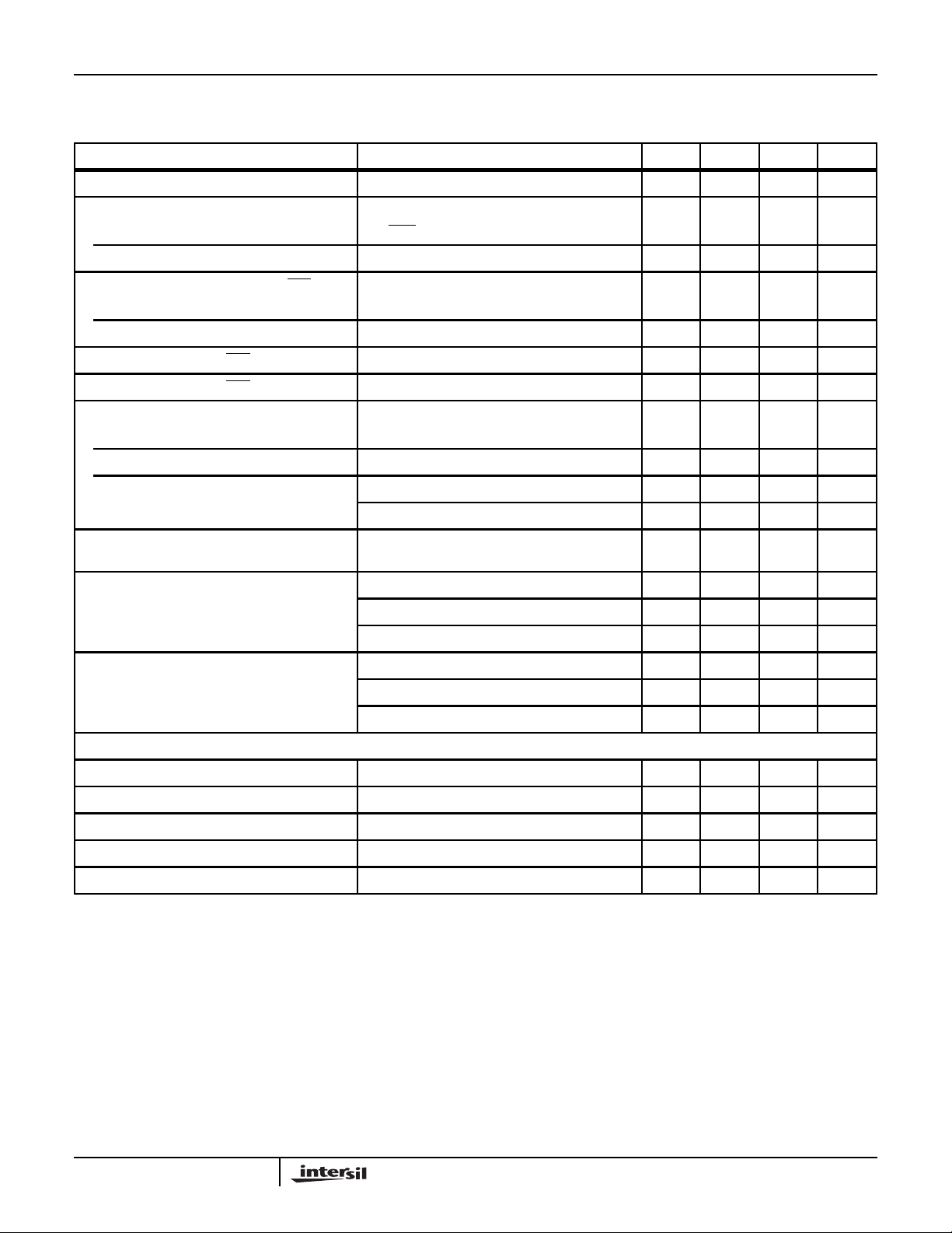
Electrical Specifications Unless Otherwise Specified, Typical Parameters are at T
PARAMETER TEST CONDITIONS MIN TYP MAX UNITS
=25oC Thermal Information
A
Thermal Resistance (Typical, Note 1) θJA(oC/W)
PLCC . . . . . . . . . . . . . . . . . . . . . . . . . . . . . . . . . . . . 55
SOIC . . . . . . . . . . . . . . . . . . . . . . . . . . . . . . . . . . . . 70
Maximum Junction Temperature Plastic . . . . . . . . . . . . . . . . .150oC
Maximum Storage Temperature Range. . . . . . . . . . -65oC to 150oC
Maximum Lead Temperature (Soldering 10s) . . . . . . . . . . . . .300oC
(SOIC, PLCC - Lead Tips Only)
Die Characteristics
Transistor Count. . . . . . . . . . . . . . . . . . . . . . . . . . . . . . . . . . . . . .224
Diode Count. . . . . . . . . . . . . . . . . . . . . . . . . . . . . . . . . . . . . . . . . .28
Die Dimensions . . . . . . . . . . . . . . . . . . . . . . . . . . . . . . . . . 174 x 120
Substrate Potential. . . . . . . . . . . . . . . . . . . . . . . . . . . . . . . . . . .V
Process . . . . . . . . . . . . . . . . . . . . . . . . . . . . . . . . . . . . . . .Bipolar-DI
ESD (Human Body Model) . . . . . . . . . . . . . . . . . . . . . . . . . . . .500V
. Failure to do so may result in premature failure of the part. If a user wishes
BAT
Operating TemperatureRange, V
at 600Ω 2-Wire terminating impedance.
= -24V,VCC= +5V,AGND = BGND = 0V. All AC Parametersare specified
BAT
= 25oC, Min-Max Parameters are over
A
BAT
RINGING TRANSMISSION PARAMETERS
Input Impedance (Note 3) - 5.4 - kΩ
V
RING
4-Wire to 2-Wire Gain V
AC TRANSMISSION PARAMETERS
RX Input Impedance 300Hz to 3.4kHz (Note 3) - 108 - kΩ
TX Output Impedance 300Hz to 3.4kHz (Note 3) - - 20 Ω
4-Wire Input Overload Level 300Hz to 3.4kHz R
2-Wire Return Loss Matched for 600Ω (Note 3)
SRL LO 26 35 - dB
ERL 30 40 - dB
SRL HI 30 40 - dB
2-Wire Longitudinal to Metallic Balance
Off Hook
4-Wire Longitudinal Balance Off Hook 300Hz to 3400Hz (Note 3) 50 55 - dB
Low Frequency Longitudinal Balance I
Longitudinal Current Capability I
Insertion Loss 0dBm at 1kHz, Referenced 600Ω
2-Wire/4-Wire (Includes external transhybrid
amplifier with a gain of 3)
to Vt-r (Note 3) - 40 - V/V
RING
= 1200Ω, 600Ω Reference
(Note 3)
Per ANSI/IEEE STD 455-1976 (Note 3)
300Hz to 3400Hz
= 40mA TA = 25oC (Note 3) - 10 23 dBrnC
LINE
= 40mA TA = 25oC (Note 3) - - 40 mA
LINE
L
+1.0 - - V
58 63 - dB
- ±0.05 ±0.2 dB
PEAK
RMS
4-Wire/2-Wire - ±0.05 ±0.2 dB
4-Wire/4-Wire (Includes external transhybrid
amplifier with a gain of 3)
--±0.25 dB
61

HC5517
Electrical Specifications Unless Otherwise Specified, Typical Parameters are at T
Operating TemperatureRange, V
= -24V,VCC= +5V,AGND = BGND = 0V. All AC Parametersare specified
BAT
= 25oC, Min-Max Parameters are over
A
at 600Ω 2-Wire terminating impedance. (Continued)
PARAMETER TEST CONDITIONS MIN TYP MAX UNITS
Frequency Response 300Hz to 3400Hz (Note 3) Referenced to
- ±0.02 ±0.06 dB
Absolute Level at 1kHz, 0dBm Referenced 600Ω
Level Linearity Referenced to -10dBm (Note 3)
2-Wire to 4-Wire and 4-Wire to 2-Wire +3 to -40dBm - - ±0.08 dB
-40 to -50dBm - - ±0.12 dB
-50 to -55dBm - - ±0.3 dB
Absolute Delay (Note 3)
2-Wire/4-Wire 300Hz to 3400Hz - - 1.0 µs
4-Wire/2-Wire 300Hz to 3400Hz - - 1.0 µs
4-Wire/4-Wire 300Hz to 3400Hz - 0.95 1.5 µs
Transhybrid Loss V
Total Harmonic Distortion
2-Wire/4-Wire, 4-Wire/2-Wire, 4-Wire/4-Wire
Idle Channel Noise
2-Wire and 4-Wire
= 1V
IN
Reference Level 0dBm at 600Ω
300Hz to 3400Hz (Note 3)
(Note 3)
C-Message
at 1kH (Notes 3, 4) 30 40 dB
P-P
- - -50 dB
- 3 - dBrnC
Psophometric (Note 3) - -87 - dBmp
Power Supply Rejection Ratio (Note 3)
to 2-Wire 20 40 - dB
V
CC
to 4-Wire 20 40 - dB
V
CC
to 2-Wire 20 40 - dB
V
BAT
to 4-Wire 20 50 - dB
V
BAT
to 2-Wire (Note 3)
V
CC
to 4-Wire 20 28 - dB
V
CC
to 2-Wire 20 50 - dB
V
BAT
to 4-Wire 20 50 - dB
V
BAT
30Hz to 200Hz, RL = 600Ω
30 40 - dB
200Hz to 16kHz, RL = 600Ω
DC PARAMETERS
Loop Current Programming
Limit Range 20
-60mA
(Note 5)
Accuracy 10 - - %
Loop Current During Power Denial R
= 200Ω - ±4 ±7mA
L
Fault Currents
TIP to Ground (Note 3) -30-mA
RING to Ground - 120 - mA
TIP and RING to Ground (Note 3) - 150 - mA
Switch Hook Detection Threshold -1215mA
Ring Trip Comparator Voltage Threshold -0.28 -0.24 -0.22 V
Thermal
ALARM Output (Note 3) Safe Operating Die Temperature Exceeded 140 - 160
o
C
62

HC5517
Electrical Specifications Unless Otherwise Specified, Typical Parameters are at T
Operating TemperatureRange, V
= -24V,VCC= +5V,AGND = BGND = 0V. All AC Parametersare specified
BAT
= 25oC, Min-Max Parameters are over
A
at 600Ω 2-Wire terminating impedance. (Continued)
PARAMETER TEST CONDITIONS MIN TYP MAX UNITS
Dial Pulse Distortion (Note 3) - 0.1 0.5 ms
Uncommitted Relay Driver
On Voltage V
OL
IOL (RDO) = 30mA - 0.2 0.5 V
Off Leakage Current - ±10 ±100 µA
TTL/CMOS Logic Inputs (F0, F1, RS,
Logic ‘0’ V
Logic ‘1’ V
Input Current (F0, F1, RS,
Input Current (F0, F1, RS,
IL
IH
TST, RDI) IIH, 0V ≤ VIN≤ 5V - - -1 µA
TST, RDI) IIL, 0V ≤ VIN≤ 5V - - -100 µA
TST, RDI)
0 - 0.8 V
2.0 - 5.5 V
Logic Outputs
Logic ‘0’ V
Logic ‘1’ V
OL
OH
Power Dissipation On Hook V
Power Dissipation Off Hook V
I
= 800µA - 0.1 0.5 V
LOAD
I
= 40µA 2.7 - - V
LOAD
CC
V
CC
CC
= +5V, V
= +5V, V
= +5V, V
= -80V, R
BAT
= -48V, R
BAT
= -24V, R
BAT
= ∞ - 300 - mW
LOOP
= ∞ - 150 - mW
LOOP
LOOP
= 600Ω,
- 280 - mW
IL = 25mA
I
CC
I
BAT
VCC = +5V, V
= +5V, V
V
CC
= +5V, V
V
CC
= -80V, R
BAT
= -48V, R
BAT
= -24V, R
BAT
VCC = +5V, VB- = -80V, R
= +5V, VB- = -48V, R
V
CC
= +5V, VB- = -24V, R
V
CC
= ∞ -36mA
LOOP
= ∞ -25mA
LOOP
= ∞ - 1.9 4 mA
LOOP
= ∞ - 3.6 7 mA
LOOP
= ∞ - 2.6 6 mA
LOOP
= ∞ - 1.8 4 mA
LOOP
UNCOMMITTED OP AMP PARAMETERS
Input Offset Voltage - ±5-mV
Input Offset Current - ±10 - nA
Differential Input Resistance (Note 3) - 1 - MΩ
Output Voltage Swing (Note 3) R
= 10kΩ - ±3-V
L
P-P
Small Signal GBW (Note 3) - 1 - MHz
NOTES:
3. These parameters are controlled by design or process parameters and are not directly tested. These parameters are characterized upon initial
design release, upon design changes which would affect these characteristics, and at intervals to assure product quality and specification compliance.
4. For transhybrid circuit as shown in Figure 10.
5. Application limitation based on maximum switch hook detect limit and metallic currents. Not a part limitation.
63

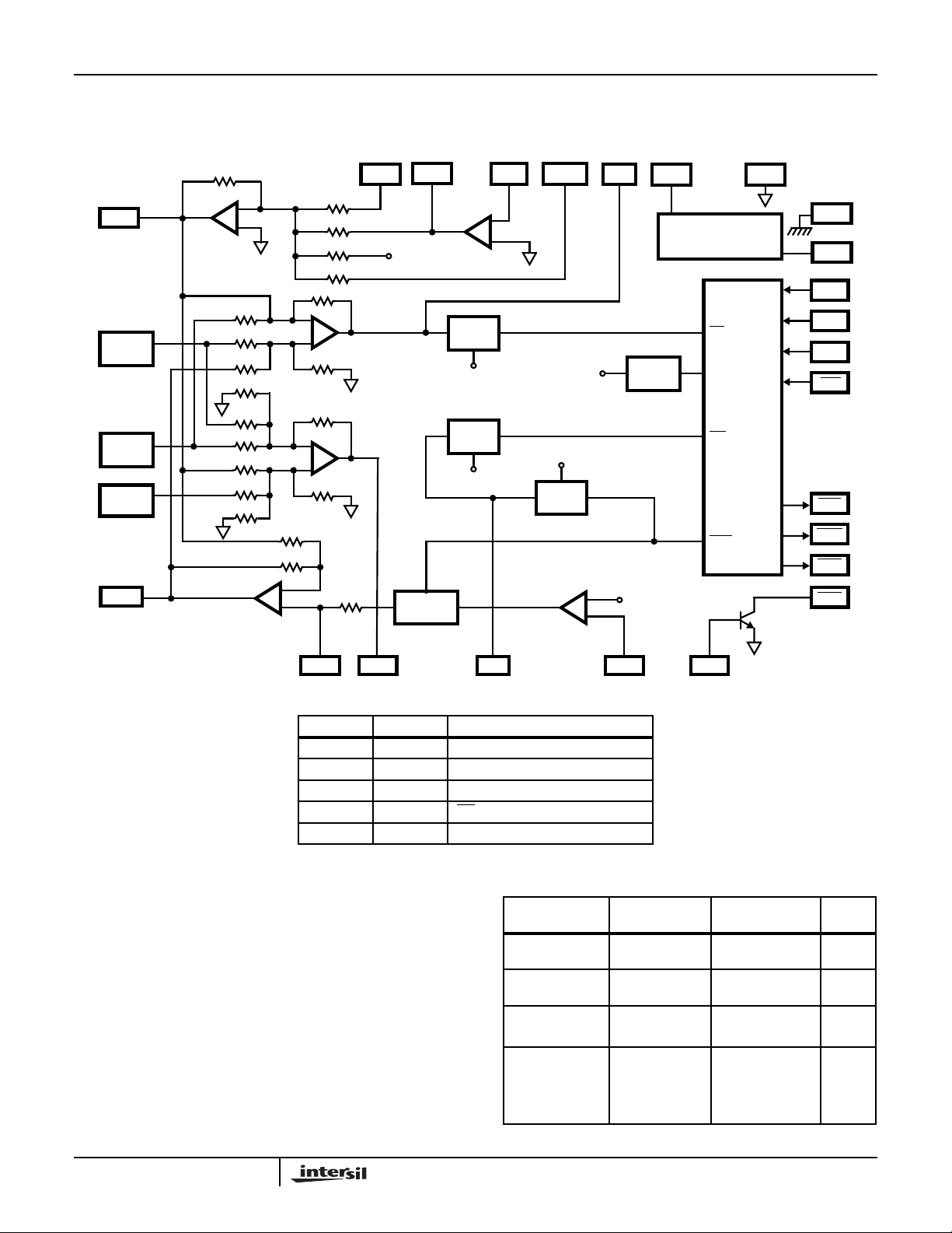
Functional Diagram
HC5517
PLCC/SOIC
TF
TIP
SENSE
RING
SENSE 1
RING
SENSE 2
RF
R
TF
25
14
15
16
26
-
+
100K
100K
100K
100K
R
R
R
R
4.5K
4.5K
RF
2R
-
+
2R
25K
-
+
25K
90K
90K
-
+
VRX
R
R
R/2
R/20
TA
RA
90K
OUT 1
17 12
+2V
VB/2
REF
SHD
RTD
-
+
-IN 1
OP AMP
V
RING
13 24 19 2
FAULT
DET
GM
V
+
TX
THERM
LTD
RF2
V
CC
BIAS
NETWORK
SH
TSD
GK
RFC
AGND
IIL LOGIC INTERFACE
1
22
BGND
27
V
BAT
4
F1
5
F0
6
RS
9
TST
7
SHD
8
RTD
10
ALM
21
RDO
R = 108kΩ
V
REF
3
18
HC5517 TRUTH TABLE
F1 F0 ACTION
0 0 Loop power Denial Active
0 1 Power Down Latch RESET
0 1 Power on RESET
10
1 1 Normal Loop feed
Over Voltage Protection and Longitudinal Current
Protection
The SLIC device, in conjunction with an external protection
bridge, will withstand high voltage lightning surges and
power line crosses.
High voltage surge conditions are as specified in Table 1.
The SLIC will withstand longitudinal currents up to a
maximum or 30mA
RMS
, 15mA
per leg, without any
RMS
performance degradation
.
28
RTINU ILMT
RD Active
PARAMETER
Longitudinal
Surge
Metallic Surge 10µs Rise/
T/GND 10µs Rise/
R/GND
50/60Hz Current
T/GND 11 Cycles 700 (Plastic) V
R/GND Limited to
11
TABLE 1.
TEST
CONDITION
10µs Rise/
1000µs Fall
1000µs Fall
1000µs Fall
10A
RMS
20
RDI
PERFORMANCE
(MAX) UNITS
±1000 (Plastic) V
±1000 (Plastic) V
±1000 (Plastic)
PEAK
PEAK
PEAK
RMS
64

HC5517
Circuit Operation and Design Information
The HC5517 is a voltage feed current sense Subscriber Line
Interface Circuit (SLIC). This means that for long loop appli-
cations the SLIC provides a constant voltage to the tip and
ring terminals while sensing the tip to ring current. For short
loops, where the loop current limit is exceeded, the tip to ring
voltage decreases as a function of loop resistance.
The following discussion separates the SLIC’s operation into
its DC and AC path, then follows up with additional circuit
design and application information.
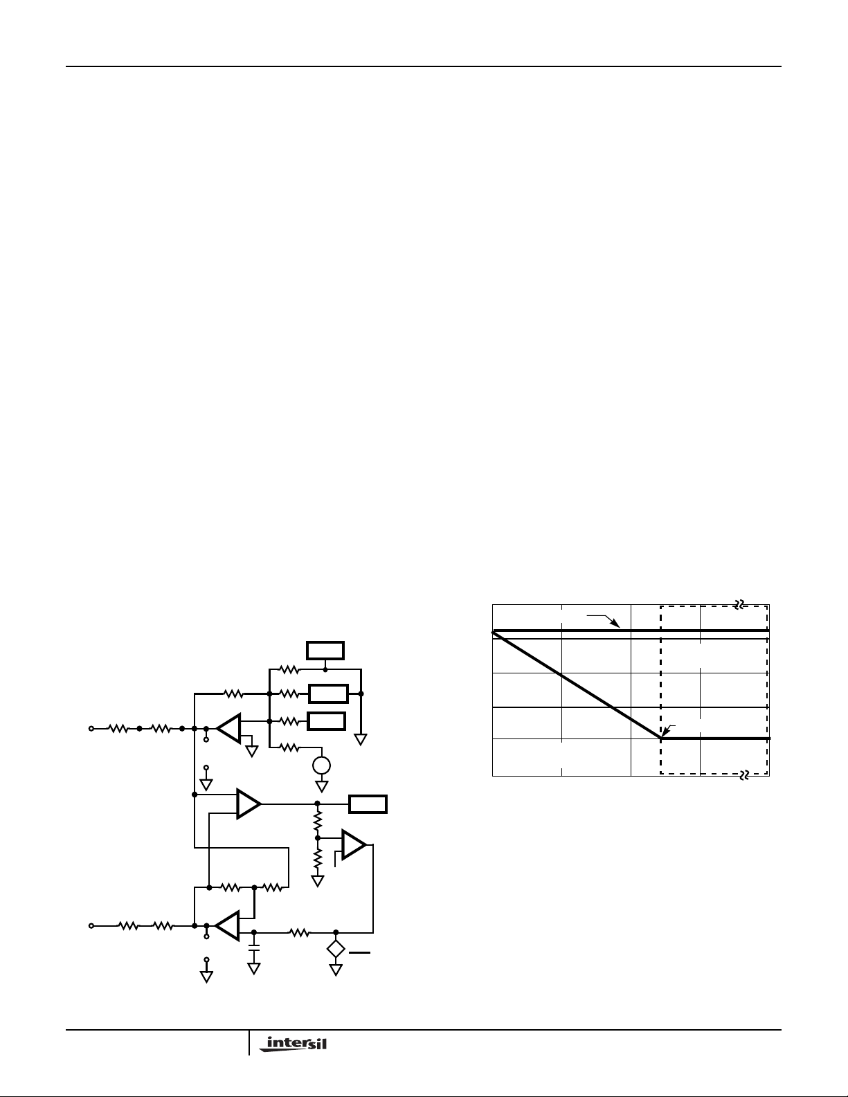
DC Operation of Tip and Ring Amplifiers
SLIC in the Active Mode
The tip and ring amplifiers are voltage feedback op amps
that are connected to generate a differential output (e.g. if tip
sources 20mA then ring sinks 20mA). Figure 1 shows the
connection of the tip and ring amplifiers. The tip DC voltage
is set by an internal +2V reference, resulting in -4V at the
output. The ring DC voltage is set by the tip DC output voltage and an internal V
at the output. (See Equation 1, Equation 2 and Equation 3.)
V
TIPFEEDVC
V
RINGFEEDVD
==
/2 reference, resulting in V
BAT
R
-----------
2V–
R2⁄
V
BAT
-------------- -
2
4V–== =
R
1
V
--- -+
–
R
TIPFEED
R
--- -
R
BAT
(EQ. 1)
(EQ. 2)
+4V
Current Limit
The tip feed to ring feed voltage (Equation 1 minus
Equation 3) is equal to the battery voltage minus 8V. Thus,
with a 48 (24) volt battery and a 600Ω loop resistance,
including the feed resistors, the loop current is 66.6mA
(26.6mA). On short loops the line resistance often
approaches zero and the need exists to control the
maximum DC loop current.
Current limiting is achieved by a feedback network (Figure 1)
that modifies the ring feed voltage (V
) as a function of the
D
loop current. The output of the Transversal Amplifier (TA) has
a DC voltage that is directly proportional to the loop current.
This voltage is scaled by R
and R28. The scaled voltage is
10
the input to a transconductance amplifier (GM) that
compares it to an internal reference level. When the scaled
voltage exceeds the internal reference level, the
transconductance amplifier sources current. This current
charges C
voltage (V
effectively reduces the tip feed to ring feed voltage (V
in the positive direction causing the ring feed
16
) to approach the tip feed voltage (VC). This
D
T-R
and holds the maximum loop current constant.
The maximum loop current is programed by resistors R
10
and R28as shown in Equation 4 (Note: R10is typically
100kΩ).
I
LIMIT
0.6()R10R28+()
---------------------------------------------=
()
200xR
28
(EQ. 4)
),
V
RINGFEEDVDVBAT
R
TIP
RING
V
, V
OUT1
GROUNDED FOR
DC ANALYSIS
R
11
R
RX
13
R
14
12
4+==
R
TIP FEED
-
+
-
V
C
+
TRANSVERSAL
AMP
90kΩ 90kΩ
RING FEED
-
+
+
V
D
-
(EQ. 3)
V
RX
R
R
OUT1
R/20
V
RING
R/2
INTERNAL
+
-
+2V REF
TA
-
+
R
10
R
28
90kΩ
C
16
RF2
V
TX
GM
-
+
V
-
BAT
+
2
FIGURE 1. OPERATION OF THE TIP AND RING AMPLIFIERS
0
V
TIP FEED
-5
-10
-15
-20
TIP AND RING VOLTAGE (V)
-25
CURRENT LIMIT
REGION I
0
FIGURE 2. V
Figure 2 illustrates the relationship between V
= -4V
= 25mA
LOOP
250
LOOP RESISTANCE (Ω)
vs RL(V
T-R
CONSTANT VOLTAGE
V
RING FEED
500 750
= -24V, I
BAT
LIMIT
REGION
= 25mA)
T-R
= -20V
∞
and the
loop resistance. The conditions are shown for a battery voltage of -24V and the loop current limit set to 25mA. For a infinite loop resistance both tip feed and ring feed are at -4V
and -20V respectively. When the loop resistance decreases
from infinity to about 640Ω the loop current (obeying Ohm’s
Law) increases from 0mA to the set loop current limit. As the
loop resistance continues to decrease, the ring feed voltage
approaches the tip feed voltage as a function of the programed loop current limit (Equation 4).
65
 Loading...