

HC5503
Low Cost 24V SLIC For PABX/Key
Systems
The Intersil HC5503 low cost SLIC is optimized for use in
small Analog or mixed Analog and Digital Key Telephone
Systems (KTS) or PBX products. The low component count
solution and surface mount package options,enable a small
desktop Key System/PBX product to be achieved. The
internal power dissipationofthe end product is minimized by
the low power consumption and minimal power supply
voltage requirements of the HC5503.
The HC5503 integrated solution provides higher quality,
higher reliability and better performance solution than a
transformer, thick film hybrid or discrete analog subscriber
interface design.
The HC5503 is designed in a Dielectrically isolated bipolar
technology andisinherently latch proof and doesnot require
hot plug or power supply sequencing precautions.
March 1999 File Number
4344.3
Description
• Wide Operating Battery Range (-21V to -44V)
• Single Additional +5V Supply
• 25mA Short Loop Current Limit
• Ring Relay Driver
• Switch Hook and Ring Trip Detect
• Low On-Hook Power Consumption
• On-Hook Transmission
• ITU-T Longitudinal Balance Performance
• Loop Power Denial Function
• Thermal Protection
• Supports Tip, Ring or Balanced Ringing Schemes
• Low Profile SO and PLCC Surface Mount Packaging
• Pin Compatible with Industry Standard HC5504B SLIC
Ordering Information
TEMP.
PART NUMBER
HC5503CM 0 to 75 28 Ld PLCC N28.45
HC5503CB 0 to 75 24 Ld SOIC M24.3
RANGE (oC) PACKAGE
PKG.
NO.
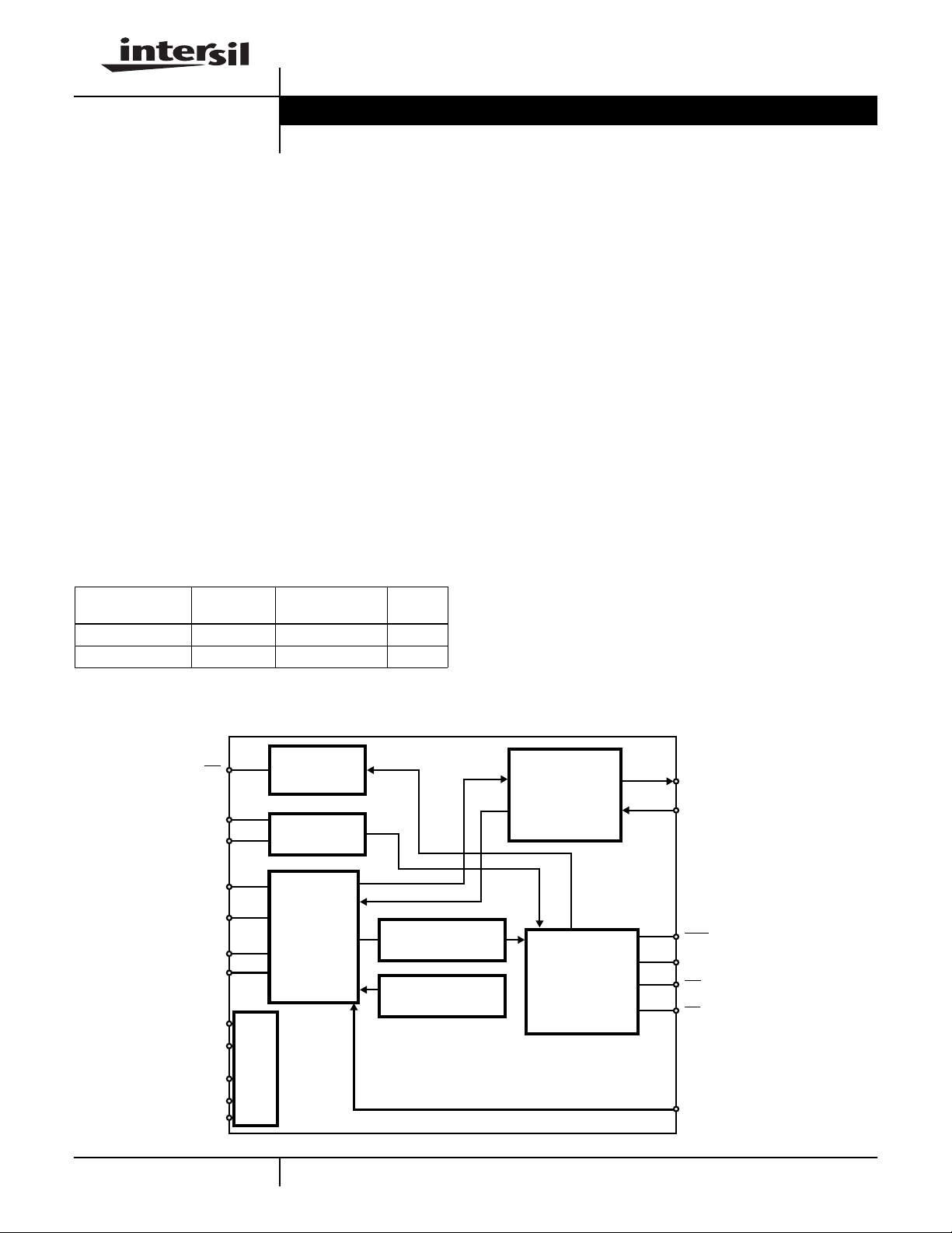
Block Diagram
BIAS
RING RELAY
DRIVER
RING TRIP
DETECTOR
2-WIRE
INTERFACE
LOOP CURRENT
THERMAL LIMIT
RD
RFS
C
TIP
TF
RING
RF
V
BAT
V
CC
AGND
BGND
DGND
2
DETECTOR
Applications
• Analog Subscriber Line Interfaces in Analog Key Systems
and Digital ISDN PABX Systems
• Related Literature
- AN571, Using Ring Sync with HC-5502A and HC-5504
SLICs
4-WIRE
INTERFACE
VF SIGNAL
PATH
LOGIC
INTERFACE
TX
RX
SHD
RS
RC
PD
C
1
1
CAUTION: These devices are sensitive to electrostatic discharge; follow proper IC Handling Procedures.
http://www.intersil.com or 407-727-9207 | Copyright © Intersil Corporation 1999

HC5503
Absolute Maximum Ratings (Note 1) Thermal Information
Maximum Continuous Supply Voltages
(V
). . . . . . . . . . . . . . . . . . . . . . . . . . . . . . . . . . . . . . -60 to 0.5V
BAT
(VCC) . . . . . . . . . . . . . . . . . . . . . . . . . . . . . . . . . . . . . . -0.5 to 15V
(VCC - V
) . . . . . . . . . . . . . . . . . . . . . . . . . . . . . . . . . . . . . .75V
BAT
Relay Drive Voltage (VRD). . . . . . . . . . . . . . . . . . . . . . . . -0.5 to 15V
Operating Conditions
Operating Temperature Range
HC5503 . . . . . . . . . . . . . . . . . . . . . . . . . . . . . . . . . . . 0oC to 75oC
Relay Driver Voltage (VRD) . . . . . . . . . . . . . . . . . . . . . . . .5V to 12V
Positive Supply Voltage (VCC). . . . . . . . . . . . . . . . . . 4.75V to 5.25V
Negative Supply Voltage (V
High Level Logic Input Voltage. . . . . . . . . . . . . . . . . . . . . . . . . . 2.4V
Low Level Logic Input Voltage . . . . . . . . . . . . . . . . . . . . . . . . . . 0.6V
CAUTION: Stresses above those listed in “Absolute Maximum Ratings” may cause permanent damage to the device. This is a stress only rating and operationofthe
device at these or any other conditions above those indicated in the operational sections of this specification is not implied.
NOTES:
1. Absolute maximum ratings are limiting values, applied individually, beyond which the serviceability of the circuit may be impaired. Functional
operability under any of these conditions is not necessarily implied.
2. θJA is measured with the component mounted on an evaluation PC board in free air.
) . . . . . . . . . . . . . . . . . .-22V to -26V
BAT
Thermal Resistance (Typical, Note 2) θJA (oC/W)
24 Lead SOIC . . . . . . . . . . . . . . . . . . . . . . . . . . . . . 75
28 Lead PLCC . . . . . . . . . . . . . . . . . . . . . . . . . . . . . 65
Maximum Junction Temperature . . . . . . . . . . . . . . . . . . . . . . .150oC
Maximum Storage Temperature Range. . . . . . . . . . -65oC to 150oC
Maximum Lead Temperature (Soldering 10s) . . . . . . . . . . . . .300oC
(PLCC and SOIC - Lead Tips Only)
Die Characteristics
Transistor Count. . . . . . . . . . . . . . . . . . . . . . . . . . . . . . . . . . . . . .185
Diode Count. . . . . . . . . . . . . . . . . . . . . . . . . . . . . . . . . . . . . . . . . .36
Die Dimensions . . . . . . . . . . . . . . . . . . . . . . . . . . . . . . . . . 137 x 102
Substrate Potential. . . . . . . . . . . . . . . . . . . . . . . . . . . . . . Connected
Process . . . . . . . . . . . . . . . . . . . . . . . . . . . . . . . . . . . . . . .Bipolar-DI
Electrical Specifications Unless Otherwise Specified, V
= -24V, VCC = 5V, AG = BG = DG = 0V, Typical Parameters
BAT
TA = 25oC. Min-Max Parameters are Over Operating Temperature Range
PARAMETER CONDITIONS MIN TYP MAX UNITS
On Hook Power Dissipation I
Off Hook Power Dissipation RL = 600Ω, I
Off Hook I
Off Hook I
Off Hook I
VCC
VCC
BAT
Off Hook Loop Current RL = 400Ω, I
Off Hook Loop Current RL = 400Ω, V
= 0 (Note 3), VCC = 5V - 80 100 mW
LONG
= 0 (Note 4), VCC = 5V - 180 200 mW
LONG
RL = 600Ω, I
RL = 600Ω, I
RL = 600Ω, I
= 0 (Note 3), TA = 0oC - - 6.0 mA
LONG
= 0 (Note 3), TA = 25oC - - 4.0 mA
LONG
= 0 (Notes 3, 4) - 19 23 mA
LONG
= 0 (Note 3) - 22.9 - mA
LONG
BAT
= -21.6V, I
LONG
= 0 (Note 3)
17.5 - - mA
TA = 25oC
Off Hook Loop Current RL = 200Ω, I
= 0 (Note 3) - 25 30 mA
LONG
Fault Currents
TIP to Ground (Note 4) - 27.5 - mA
RING to Ground -70- mA
TIP to RING (Note 4) - 30 - mA
TIP and RING to Ground - 140 - mA
Ring Relay Drive V
OL
IOL = 62mA - 0.2 0.5 V
Ring Relay Driver Off Leakage VRD = 12V, RC = 1 = HIGH, TA = 25oC--25µA
Ring Trip Detection Period RL = 600Ω,(Note 5) - 2 3 Ring Cycles
Switch Hook Detection Threshold 5 - 10.5 mA
Loop Current During Power Denial RL = 200Ω - ±2- mA
Dial Pulse Distortion (Note 4) 0 - 0.5 ms
Receive Input Impedance (Note 5) - 90 - kΩ
Transmit Output Impedance (Note 5) - 10 20 Ω
2

HC5503
Electrical Specifications Unless Otherwise Specified, V
= -24V, VCC = 5V, AG = BG = DG = 0V, Typical Parameters
BAT
TA = 25oC. Min-Max Parameters are Over Operating Temperature Range (Continued)
PARAMETER CONDITIONS MIN TYP MAX UNITS
2-Wire Return Loss Referenced to 600Ω +2.16µF (Note 4)
SRL LO - 15.5 - dB
ER
L
-24- dB
SRL HI -31- dB
Longitudinal Balance 1V
2-Wire Off Hook 53 58 - dB
200Hz - 3400Hz, (Note 4) IEEE Method
RMS
0oC ≤ TA≤ 75oC
2-Wire On Hook 53 58 - dB
4-Wire Off Hook at 1kHz 50 58 - dB
Insertion Loss 0dBm Input Level, Referenced 600Ω
2-Wire to 4-Wire at 3.4kHz
VTR to V
O
VO is the Output of the Transhybrid
Amplifier - ±0.05 ±0.2 dB
4-Wire to 2-Wire at 300Hz -3.8 -4.0 -4.2 dB
Frequency Response 200 - 3400Hz Referenced to Absolute Loss at 1kHz
- ±0.02 ±0.05 dB
and 0dBm Signal Level (Note 4)
Idle Channel Noise
2-Wire to 4-Wire
Idle Channel Noise
4-Wire to 2-Wire
(Note 4)
- 1 5 dBrnC
- -89 -85 dBm0p
- 1 5 dBrnC
- -89 -85 dBm0p
Absolute Delay (Note 5)
2-Wire to 4-Wire, 4-Wire to 2-Wire - - 2 µs
Trans Hybrid Loss Balance Network Set Up for 600Ω Termination at
30 40 - dB
1kHz
Overload Level VCC = +5V
2-Wire to 4-Wire (On-hook) 2.5 - - V
4-Wire to 2-Wire (Off-hook, RL = 600Ω) 3.1 - - V
PEAK
PEAK
Level Linearity At 1kHz, (Note 4) Referenced to 0dBm Level
2-Wire to 4-Wire, 4-Wire to 2-Wire +3 to -40dBm - - ±0.05 dB
-40 to -50dBm - - ±0.1 dB
-50 to -55dBm - - ±0.3 dB
Power Supply Rejection Ratio (Note 4)
VCC to 2-Wire 35 - - dB
30 - 60Hz, RL = 200Ω
VCC to Transmit 35 - - dB
V
to 2-Wire 20 - - dB
BAT
V
to Transmit 20 - - dB
BAT
VCC to 2-Wire 200 - 16kHz, RL = 200Ω 35 - - dB
VCC to Transmit 35 - - dB
V
to 2-Wire 35 - - dB
BAT
V
to Transmit 35 - - dB
BAT
Logic Input Current (RS, RC, PD) 0V ≤ VIN≤ 2.4V - - ±20 µA
3
HC5503
Electrical Specifications Unless Otherwise Specified, V
TA = 25oC. Min-Max Parameters are Over Operating Temperature Range (Continued)
PARAMETER CONDITIONS MIN TYP MAX UNITS
Logic Inputs
Logic ‘0’ V
Logic ‘1’ V
SHD Output
Logic ‘1’ V
NOTES:
3. I
LONG
4. These parameters are controlled by design or process parameters and are not directly tested. These parameters are characterized upon initial
design release, upon design changes which would affect these characteristics, and at intervals to assure product quality and specification compliance.
5. Guaranteed by design, not tested.
IL
IH
OL
OH
= Longitudinal Current.
I
800µA, VCC = 5VLogic ‘0’ V
LOAD
I
40µA, VCC = 5V 2.7 - 5.0 V
LOAD
= -24V, VCC = 5V, AG = BG = DG = 0V, Typical Parameters
BAT
- - 0.8 V
2.0 - 5.5 V
- 0.1 0.4 V
4
Design Information
HC5503
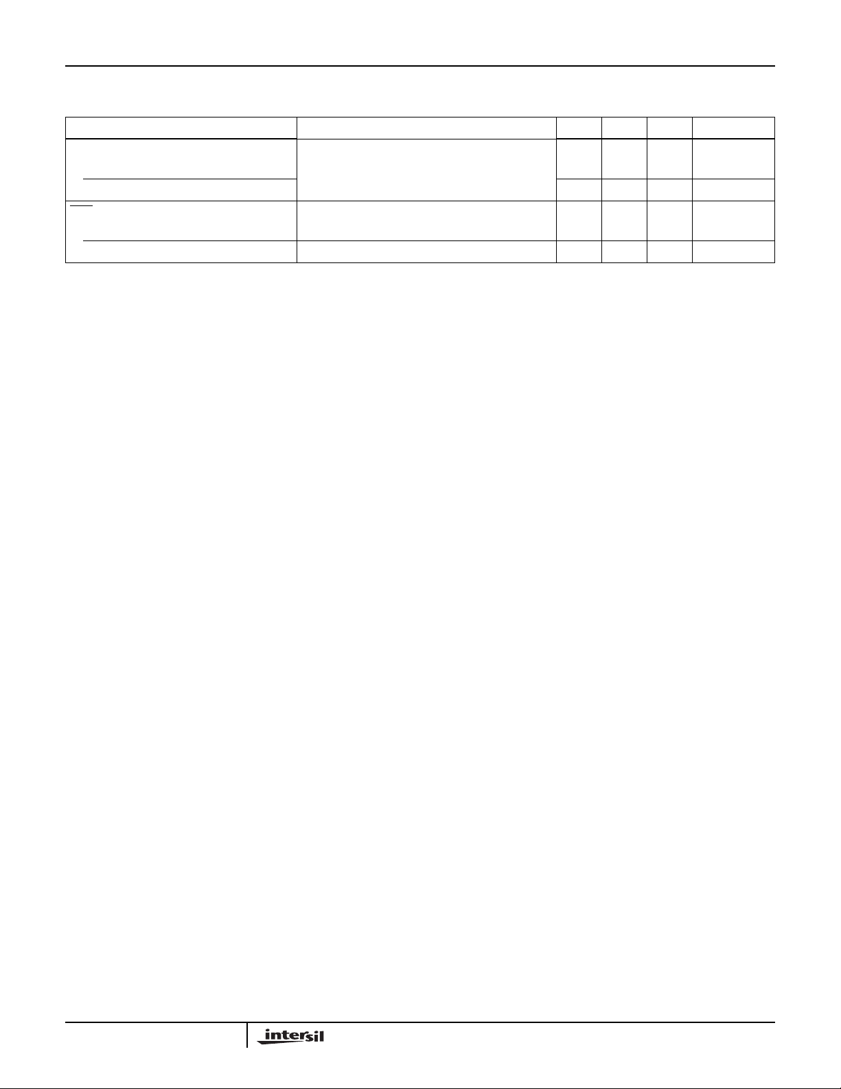
Line Feed Amplifiers
The line feed amplifiers are high power operational
amplifiers and are connected to the subscriber loop through
150Ω of feed resistance as shown in Figure 1. The feed
resistors and synthesized impedance via feedback provide a
600Ω balanced load for the 2-wire to 4-wire transmission.
The tip feed amplifier is configured as a unity gain
noninverting buffer. A -4V bias (derived from the negative
battery (V
the amplifier. Hence, the tip feed DC level is at -4V. The
principal reason for this offset is to accommodate sourcing
and sinking of longitudinal noise currents up to 15mA
without saturating the amplifier output and to provide
sufficient overhead for receive signals. The tip feed amplifier
also feeds the ring feed amplifier, which is configured as a
unity gain inverting amplifier as seen from the tip feed
amplifier. The noninverting input to the ring feed amp is
biased at a V
has a noninverting gain of 2. Thus, the DC output at ring
feed is:
V
(DC) = (4 + V
RF
For a -24V battery, VRF = -20V. Hence, the nominal battery
feed across the loop provided by the SLIC is 16V. When the
subscriber goes off-hook this DC feed causes current
(metallic current) to flow around the loop.
) in the bias network) is applied to the input of
BAT
/2. Looking into this terminal the amplifier
BAT
) Volts
BAT
RMS
The received audio signal R
is fed into the tip feed amplifier
X
and appears at the tip feed terminal. It is also fed through the
ring feed amplifier and is inverted. Thus, a differential signal of
2V
appears between tip feed and ring feed. The RX signal
RX
causes AC audio currents to flow around the loop which are
then AC coupled to the earpiece of the telephone set.
2-Wire Impedance Matching
The HC5503 is optimized for operation with a -24V battery.
Impedance matching to a 600Ω load, is achieved through
the combination of the feed resistors (R
negative feedback through resistor R
R
and RB2 are sense resistors that detect loop current
B1
and provide negative feedback to synthesize the remaining
300Ω required to match a 600Ω line.
The impedance looking into the tip terminal is 150Ω (R
plus the synthesized impedance of the tip amplifier. The
synthesized tip impedance is equal to the tip feed voltage Va
divided by ∆IL. (Note, the tip feed amplifier is a voltage
follower. Thus, the tip feed voltage is equal to the receive
input voltage V
, both are labeled Va.) The synthesized
RX
impedance of the ring terminal is calculated the same way
and is the ring feed voltage divided by ∆IL. (Note, the ring
feed voltage is equal in magnitude to the tip feed voltage, but
opposite in phase as a result of the ring feed amplifier gain.)
, RB2) and
B1
(reference Figure 1).
2
B1
)
∆I
+
L
-
TIP
Z
IN
RB1 = RB2 = RS = 150Ω
RING
NOTE: Grounded for AC analysis.
R
150Ω
R
150Ω
- ∆I
B2
B1
+
L
TIP FEED
RING FEED
Va
C
4RS∆I
3
TX
L
+
4V
DC
(NOTE)
HC5503
RX
+
2
-
L
+
-
RR
-
+
FIGURE 1. IMPEDANCE MATCHING CIRCUITRY
90kΩ
-
+
+
-
-
+
+4RS∆I
V
-
BAT
+
2
(NOTE)
TO TRANSHYBRID OP-AMP
R
3
R
1
V
IN
R
2
C
4
INPUT
FROM
CODEC
5

HC5503
The value of Va, as a result of feedback through R2from the
T
output, is given in Equation 1. Equation 1 is a voltage
X
divider equation between resistors R
combination of resistors; R
resistor R
INTERNAL
. The Voltage on the transmit out (TX) is
, R3 and the internal 90kΩ
1
the sum of the voltage drops across resistors R
and the parallel
2
B1
and R
B2
that is gained up by 2 to produce an output voltage at the
V
pin that is equal to -4RS∆IL.
TX
R190kΩ R
-------------------------------------------------
V
a
R190kΩ R3R2+
3
×=
V
TX
(EQ. 1)
Where: VTX = -4RS∆IL = -600∆IL.
To match a 600Ω line, the synthesized tip and ring impedance
must be equal to 150Ω. The impedance looking into either the
tip or ring terminalis once again the voltage at the terminal(Va)
divided by the AC current∆IL as shown in Equation 2.
V
Z
TipfeedZRingfeed
Substituting the value of 600∆IL for V
a
-------- 150Ω===
∆I
L
TX
(EQ. 2)
in Equation 1 and
dividing both sides by ∆IL results in Equation 3.
R
V
a
--------
∆I
L
Setting Va/∆IL equal to 150Ω and solving for R
R
= 10kΩ,R
1
R
to match the input impedance of 600Ω is determined to
2
90kΩ R
1
-------------------------------------------------
R190kΩ R3R2+
3
INTERNAL
600×=
(EQ. 3)
, given that
2
= 90kΩ and R3= 150kΩ the value of
be 25.47kΩ. (Note: nearest standard value is 24.9kΩ).
The amount of negative feedback is dependent upon the
additional synthesized resistance required for matching. The
sense resistors R
maintain the
and RB2 should remain at 150Ω to
B1
SHD threshold listed in the electrical
specifications. The additional synthesized resistance is
determined by the feed back factor X (Equation 4) which
needs to be applied to the transmit output and fed into the
RX pin of the HC5503. The feed back factor is equal to the
voltage divider between R2 and the parallel combination of
R
, R3 and R
1
FeedbackFactor X
R
X
INTERNAL
HC5503
24.9kΩ
T
X
T
X
, reference Figure 2.
-------------------------------------------------==
R190kΩ R3R2+
FEED BACK
R
2
= -4RS∆IL
R
1
R
150kΩ
90kΩ R
3
3
R
1
10kΩ
R
INTERNAL
90.0kΩ
(EQ. 4)
The voltage that is feed back into the RX pin is equal to the
voltage at V
VaVTXX()=
Where V
times the feedback factor (Equation 5).
TX
is equal to -4RS∆IL (RS = 150Ω)
TX
(EQ. 5)
So:
V
X
a
------------------ -=
∆IL600
(EQ. 6)
But, from Equation 2:
V
a
-------- 150Ω=
∆I
L
(EQ. 7)
Therefore:
V
150
--------- -
600
1
-- -===
4
output voltage is
X
(EQ. 8)
a
X
---------- -
V
TX
Equation 8 shows that 1/4 of the T
required to synthesize 150Ω at both the Tip feed and Ring
feed amplifiers.
To match a 900Ω load would require 300Ω worth of
synthesized impedance (300Ω from R
+ RB2 and 600Ω
B1
from the Tip feed + Ring feed amplifiers).
Setting Va/∆ILequal to 300Ω and solving for R
given that R
the value of R
= 10kΩ, R
1
to match the input impedance of 900Ω is
2
INTERNAL
= 90kΩ and R3= 150kΩ
in Equation 3,
2
determined to be 8.49kΩ (Note: nearest standard value is
8.45kΩ). The feed back factor to match a 900Ω load is 1/2
(300/600).
The selection of the value of 150kΩ for R
is arbitrary. The
3
only requirement is that it be large enough to havelittle effect
on the parallel combination between R
R
(10kΩ). R3 should be greater then 90kΩ.
1
INTERNAL
(90kΩ) and
The selection of the value of 10kΩ for R1 is also arbitrary.
The only requirement is that the value be small enough to
offset any process variations of R
INTERNAL
and large
enough to avoid loading of the CODEC’s output. A value of
10kΩ is a good compromise.
2-Wire to 4-Wire Gain
The 2-wire to 4-wire gain is defined as the output voltage
V
divided by the tip to ring voltage (VTR). Where:
TX
V
=-4RS∆IL = -600∆IL and VTR = (RL)∆IL = 600∆IL.
TX
The 2-wire to 4-wire gain is therefore equal to -1.0, as
shown in Equation 9.
24–
V
-----------
V
A
600– ∆I
TX
---------------------- 1.0–== =
600∆I
TR
L
L
(EQ. 9)
FIGURE 2. FEEDBACK EQUIVALENT CIRCUIT
6

4-Wire to 2-Wire Gain
The 4-wire to 2-wire gain is defined as the output voltage
V
divided by the input voltage, VIN. To determine the
TR
4-wire to 2-wire gain we need to define V
The voltage at V
impedance Z
V
∆ILZL×∆ILZO×==
TR
is the loop current times the load
TR
.
L
For optimum 2-wire return loss, the input impedance of the
SLIC (Z
Equations going further assume Z
) must equal the load impedance (ZL) of the line. All
O
= ZO.
L
The loop current ∆IL is the total voltage across the loop
divided by the total resistance of the loop. The total voltage
across the loop is the sum of the tip feed voltage (V
the ring feed voltage (V
) where VTF= -VRF. The total
RF
resistance is the sum of the sense resistors RB
and the load ZL (ZL +2RS). The total loop current is defined
in Equation 11.
∆I
L
VTFVRF–
---------------------------+
Z
O2RS
2V
()
TF
------------------------- -==
+
Z
O2RS
From Equation 10:
V
TR
∆I
-----------=
L
Z
O
Substituting Equation 12 into Equation 11 and solving for
V
:
TR
2VTF()
V
------------------------- -
=
TR
+
Z
O2RS
Z
O
Using Superposition, the voltage at the receive input R
given as:
V
RXVTF
R′
1
---------------------- -
R′1R2+
V
TX
R′
2
---------------------- -
+==
R′2R1+
Where R′1 is the effective impedance that is formed by the
parallel combination of R
INTERNAL
(90kΩ), R3 (150kΩ), R
(10kΩ) and is equal to 8.49kΩ. R′2 is the effective
impedance that’s formed by the parallel combination of
R
INTERNAL
(90kΩ), R3 (150kΩ), R2 (24.9kΩ) and is equal
to 17.25kΩ.
in terms of VIN.
TR
and RB
1
V
IN
(EQ. 10)
) and
TF
(EQ. 11)
(EQ. 12)
(EQ. 13)
is
X
(EQ. 14)
2
HC5503
1
V
for the recommended values of R1 and R2 is given in
RX
Equations 15 and 16. For impedance matching to a load
other than 600Ω, recalculate the parallel impedances R′
R′
and substitute into Equation 15. The 4-wire to 2-wire
2
gain is recalculated by using the Equations below.
V
RXVTF
V
RXVTF
8.49kΩ
----------------------------------------------
8.49kΩ 24.9kΩ+
0.25()V
TX
+==
0.633()V
V
TX
IN
17.25kΩ
-------------------------------------------- -
+==
17.25kΩ 10kΩ+
(EQ. 15)
(EQ. 16)
Substituting Equation 16 into Equation 13:
2 0.25()V
V
-------------------------------------------------------------------------
=
TR
0.633()V
+()
TX
+
Z
O2RS
IN
Z
O
(EQ. 17)
From Equation 10:
V
TR
∆I
-----------=
L
Z
O
(EQ. 18)
From Equation 1:
V
TX
4RS∆I
–=
L
(EQ. 19)
Substituting Equation 18 into Equation 19:
V
TR
V
TX
4RS
–=
-----------
Z
O
(EQ. 20)
Substituting Equation 20 into Equation 17:
V
V
=
TR
Assuming R
300
1
----------------------- -+
Z
O
TR
-----------
– 1.266V
2RS
300+
+
Z
O
= 150Ω and rearranging terms:
S
V
1.266Z
----------------------- -
=
TR
ZO300+
The 4-wire to 2-wire gain (Given that: R
and R
= 150kΩ) for a 600Ω load is:
3
1.266Z
TR
----------------------- -
ZO600+
IN
O
42–
V
-----------
V
A
Z
O
------------------------- -
IN
ZO2RS+
O
V
IN
0.633 3.96dB–== = =
(EQ. 21)
(EQ. 22)
= 10kΩ, R2= 24.9kΩ
1
(EQ. 23)
,
1
V
IN
7

HC5503
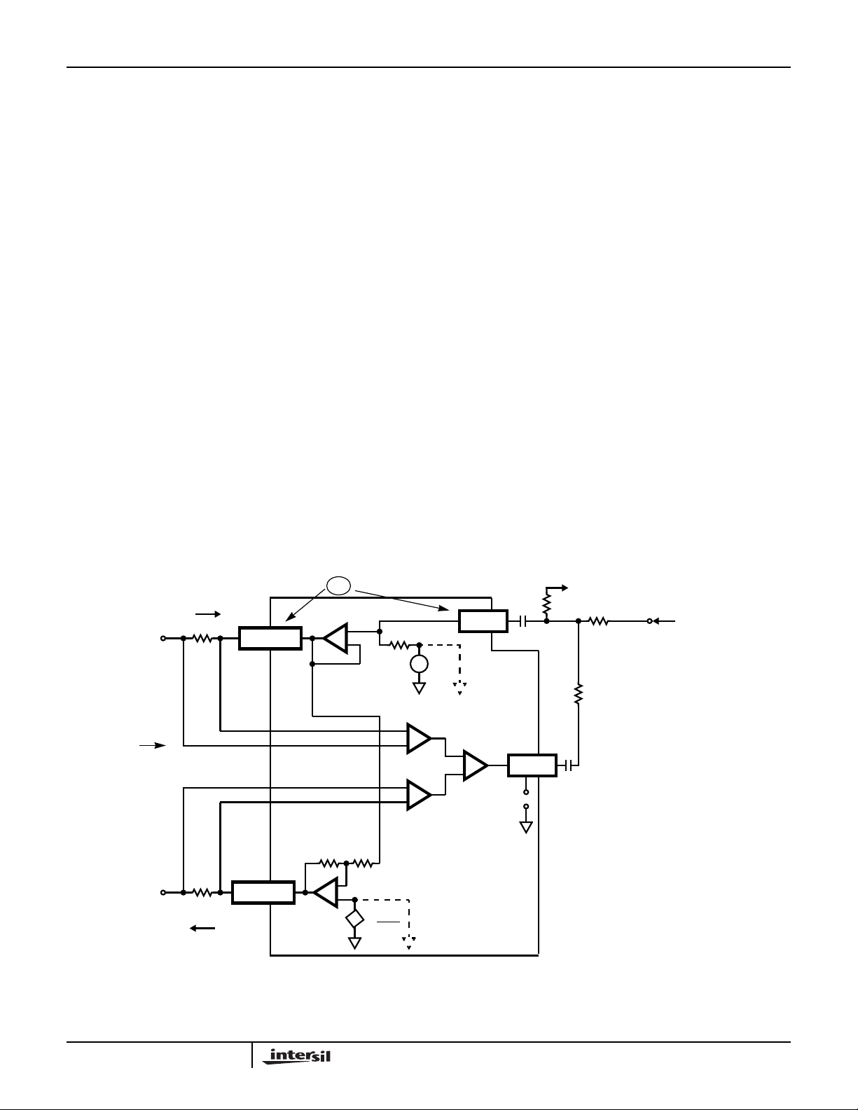
The Transversal Amplifier (TA)
Whereas the feed amplifiers perform the 4-wire to 2-wire
transmission function, the transversal amplifier acts as the
2-wire to 4-wire hybrid. The TA is a summing amplifier
configured to reject common mode signals. It will reject 2wire common mode signals. R
and RB2 act as loop
B1
current sense resistors. The voice signal output of the
amplifier is a function of the differential voltages appearing
across R
and RB2.
B1
The transversal amplifier also has a DC output proportional
to the metallic current in the loop. The output voltage is
given by:
V
TX
= 2(I
TIP
+ I
) (RB1 + RB2)
RING
This DC level is used as an input to a comparator whose
output feeds into the logic circuitryas SH. This signal is used
to gate
SHD output.
Voice signals on the loop are transformed by the TA into
ground referenced signals. Since the TA output has a DC
offset it is necessary to AC couple the output to any external
circuitry. Note, that during 4-wire to 2-wire transmission, the
transversal amplifier will have an audio signal at its output
proportional to the 4-wire audio receive signal and the loop’s
equivalent AC impedance. This is called the transhybrid
return, and must be cancelled (or balanced) out to prevent
an echo effect. Reference the Transhybrid Circuit section for
more information.
Loop Current Limiting
The maximum loop length for this application is a 533Ω load
across the feed amplifiers (24V
30mA
loop current). However, on a short loop the line
MAX
SUPPLY
resistance often approaches zero. Thus, a need exists to
control the maximum DC loop current that can flow around
the loop to prevent an excessive current drain from the
system battery. This limit is internally set to 30mA on the
HC5503. Figure 3 depicts the feedback network that
modifies the V
voltage as a function of metallic current.
RF
Figure 4 illustrates the loop current characteristics as a
function of line resistance.
As indicated above, the TA has a DC voltage output directly
proportional to the loop current. This voltage level is scaled
by R
and R18. The scaled level forms the ‘Metallic’ input
19
to one side of a Transconductance Amplifier.
- 8V
OVERHEAD
)/
V
TF
V
R
90K
R
90K
R
1.8K
21
19
= -600 I
TX
18
KV
TX
V
B5
FOR KVTX < V
LOOP
-
+
IGM > 0,
-4V
V
B
V
TX
B5
/2
V
RING
R
B1
R
B2
V
TIP
V
RF
V
RF
RING
FEED
FIGURE 3. DC LOOP CURRENT CHARACTERISTICS
TRANSVERSAL
AMP
-
+
A
VCL
-
+
= 2
C
1
The reference input to this amplifier is generated in the bias
network, and is equivalent to 30mA. When the metallic input
exceeds the set reference level, the transconductance
amplifier sources current. This current will charge C
positive direction causing the V
approach the V
(Tip Feed), effectively reducing the battery
TF
(Ring Feed) voltage to
RF
feed across the loop which will limit the DC loop current. C
in
1
1
will continue to charge until an equilibrium level is attained at
I
= I
LOOP
loop is set by R
mA (Max). The time constant of this feedback
LOOP
(90kΩ) and C1 which is nominally 0.33µF.
21
The VRF voltage level is also modified to reduce or control
loop current during ring line faults (e.g., ground or power line
crosses), and thermal overload. Figure 8 illustrates this. The
thermal and fault current circuitry works in parallel with the
transconductance amplifier.
Longitudinal Amplifier
The longitudinal amplifier is an operational amplifier
configured as a closed loop differential amplifier with a
nominal gain of 0.1. The output is a measure of any
imbalance between I
this amplifier is given by:
V
= 0.1(I
LONG
TIP
The gain factor is much less than one since ring voltage (up
to 150V
) can appear at the Ring or Ring Feed Sense
PEAK
terminals and are attenuated to avoid exceeding the
common mode range of the longitudinal amplifier’s input.
- I
TIP
RING
and I
) 150.
. The transfer function of
RING
8

HC5503
5330
R
LOOP
HC5503 I
(Ω)
30
(mA)
20
LOOP
I
= RB1 + RB2 + ZTF + ZRF + R
R
LOOP
10
FIGURE 4. DC LOOP CURRENT CHARACTERISTICS
SATURATION
LOOP
LINE
+ R
SET
The longitudinal amplifier’s principal functions is Ring Trip
Detection. The output of the amplifier after being filtered by
R
and C2 to attenuate AC signals is fed into a detector
20
whose output inhibits the ring relay driver to remove ringing
signals from the line in an off-hook condition, reference
Figure 8.
Ringing The Line
The Ring Command (RC) input is taken low during ringing.
This activates the ring relay driver (
telephone is not off-hook or the line is not in a power denial
state. The ring relay connects the ring generator to the
subscriber loop. The ring generator output is usually an
80V
, 20Hz signal. The ring signal should not exceed
RMS
150V peak. Since the telephone ringer is AC coupled only
ring current will flow. This ringing current flows directly into
via a set of relay contacts. The high impedance
V
BAT
terminal RFS is provided so that the low impedance V
node can be isolated from the hot end of the ring path in the
battery referenced ring scheme.
The AC ring current flowing in the subscriber circuit will be
sensed across RB2, and will give rise to an AC voltage at the
output of the longitudinal amplifier.R
signal before it reaches the ring trip detector to prevent false
ring trip. C
is nominally set at 1.0µF.
2
When the subscriber goes off-hook, a DC path is established
between the output of the ring generator and the battery
ground or V
terminal. A DC longitudinal imbalance is
BAT
established since no tip feed current is flowing through the
tip feed resistors. The longitudinal amplifier output is driven
negative. Once it exceeds the ring trip threshold of the ring
trip detector,the logic circuitry is driven by GK to trip the ring
relay establishing an off-hook condition such that
become active as loop metallic current starts to flow.
In addition to its ability to be used for tip or ring injected
systems, the HC5503 can also be configured for systems
utilizing balanced ringing. The main advantage of balanced
ringing is that it tends to minimizecross coupling effects owing
to the differential nature of the ring tone across the line.
Figure 5 illustrates the sequence of events during ring trip with
ring synchronization for a tip injected ring system. Note that
owing to the 90 degree phase shift introduced by the low pass
RD) output providing the
RF
and C2attenuate this
20
SHD will
filter (R
, C2) the RS pulse will occur at the most negative
20
point of the attenuated ring signal that is fed into the ring trip
detector. Hence, when DC conditions are established for
SHD,the AC component actually assists ring triptaking place.
For a ring side injected ring system, the RS pulse should
occur at the positive zero crossing of the ring signal as it
appears at RFS. If ring synchronization is not used, then the
RS pin should be held permanently to a logic high of 5V
nominally: ring trip will occur asynchronously with respect to
the ring voltage. Ring trip is guaranteed to take place within
three ring cycles after the telephone going off-hook.
It is recommended that an RC snubber network is placed
across the ring relay contacts to minimize inductive kickback effects from the telephone ringer. Typical values for
such a network are shown in Figure 10.
150V
V
RING
150V
THRESHOLD
RS
V
PEAK
MAX
C4
RING
TRIP
,
5V
0V
0V
SUBSCRIBER
GOES OFF-HOOK
FIGURE 5. RING TIP SEQUENCE
>50µs
DC SHIFT OWING TO
DC CURRENT DIFFERENCE
BETWEEN I
TIP
AND I
RING RELAY
HAS TRIPPED
RING
C
CHARGES
2
TO 0V
QUESCENT
VALUE
Transhybrid Circuit
The purpose of the transhybrid circuit is to remove the
receive signal (R
preventing an echo on the transmit side. This is
accomplished by using an external op amp (usually part of
the CODEC) and by the inversion of the signal from the
4-wire receive port (R
Figure 6 shows the transhybrid circuit. Because the voltage
is 180 degrees out of phase with the voltage at TX, the
at R
X
input signal will be subtracted from the output signal if I
equals I2. Node analysis yields the following Equation:
T
I1I2+
-------
R
X
4
The voltage at T
= 0.633) and 2-wire to 4-wire (A
(A
4-2
gains, and is therefore equal to 0.633. The voltage at R
when taking into account the negative feedback through R
) from the transmit signal (TX), thereby
X
) to the 4-wire transmit port (TX).
X
R
X
------- -+ 0==
R
3
is the product of the 4-wire to 2-wire
X
= -1.0) voltage
2-4
1
(EQ. 24)
,
X
,
2
9
HC5503
is the calculated value of 0.633 plus the feedback which is
(for matching to a 600Ω load, reference Equation 8).
1/4 T
X
The voltage at R
RX0.633
Substituting the values for T
is calculated in Equation 25.
x
1
-- -
0.633()– 0.474==
4
and RX into Equation 24 and
X
(EQ. 25)
setting the them equal to each other, the values of R3 and
can then be determined.
R
4
0.633
-------------- -
Setting the value of R
0.474
-------------- -=
R
R
4
3
to 150kΩ sets the value of R4 to be
3
(EQ. 26)
200kΩ.
Notice that the input voltage for the incoming signal (I
taken at R
, instead of the conventional method at the
X
) is
1
CODEC (point A, Figure 6). This alternative method is used
because the tolerance effects of R
on the transhybrid
1
balance are eliminated.
R
5
-
R
R
150kΩ
R
X
HC5503
T
X
FIGURE 6. TRANSHYBRID CIRCUIT
3
I
1
I
2
200kΩ
4
R
1
R
2
+
+
V
0
A
+
V
IN
-
CODEC/
FILTER
-
Power Denial (PD)
Power denial limits power to the subscriber loop: it does not
power down the SLIC, i.e., the SLIC will still consume its
normal on-hook quiescent power during a power denial
period. This function is intended to “isolate” from the battery,
under processor control, selected subscriberloops during an
overload or similar fault status.
PD
is selected, the logic circuitry inhibits RC and switches in
If
a current source to C
-3.5V at which point it is clamped. Since tip feed is always at
-4V, the battery feed across the loop is essentially zero, and
minimum loop power will be dissipated if the circuit goes offhook. No signalling functions are available during this mode.
After power denial is released (
hundred milliseconds (300ms) before the V
reaches its nominal battery setting. This is due to the RC
time constant of R
. The capacitor charges up to a nominal
1
PD
= 1), it will be several
output
RF
and C1.
21
The Logic Network
The logic network utilizes I2L logic. All external inputs and
outputs are LS TTL compatible: the relay driver is an open
collector output that can sink 60mA with a V
Figure 9 is a schematic of the combination logic within the
network. The external inputs
RC (Relay Control) and
(Power Denial) allow the switch controller to ring the line or
deny power to the loop, respectively. The Ring
Synchronization input (RS) facilitates switching of the ring
relay near a ring current zero crossing in order to minimize
inductive kickback from the telephone ringer.
Line Fault Protection
The subscriber loop can exist in a very hostile electrical
environment.It is often in close proximity to very high voltage
power lines, and can be subjected to lightning induced
voltage surges. The SLIC has to provide isolation between
the subscriber loop and the PBX/Key telephone system.
The most stringent line fault condition that the SLIC has to
withstand is that of the lightning induced surge.
The Intersil monolithic SLIC, in conjunction with a simple low
cost diode bridge, can achieve up to 450V of isolation
between the loop and switch. The level of isolation is a
function of the packaging technology and geometry together
with the chip layoutgeometries. One of the principalreasons
for using DI technology for fabricating the SLIC is that it
lends itself most readily to manufacturing monolithic circuits
for high voltage applications.
Figures 10 shows the application circuit for the HC5503. A
secondary protection diode bridge is indicated which
protects the feed amplifiers during a fault. Most line systems
will have primary protection networks. They often take the
form of a carbon block or arc discharge device. These limit
the fault voltage to less than 450V peak before it reaches the
line cards. Thus when a transient high voltage fault has
occurred, it will be transmitted as a wavefront down the line.
The primary protection network must limit the voltage to
less than 450V.
down the line towards the SLIC. The feed amplifier outputs
appear to the surge as very low impedance paths to the
system battery. Once the surge reaches the feed resistors,
fault current will flow into or out of the feed amplifier output
stages until the relevant protection diodes switch on. Once
the necessary diodes have started to conduct all the fault
current will be handled by them.
If the user wishes to characterize SLIC devices under
simulated high voltage fault conditions on the bench, he
should ensure that the negative battery power supply has
sufficient current capability to source the negative peak
fault current and low series inductance. If this is not the
case, then the battery supply could be pulled more
negative and destroy the SLIC if the total (V
voltage across it exceeds 75V.
The attenuated wave front will continue
CE
CC
of 1V.
+ V
PD
BAT
)
10

HC5503
Pin Descriptions
28 PIN
PLCC
2 1 TIP An analog input connected to the TIP (more positive) side of the subscriber loop. Functions with the Ring
3 2 RING An analog input connected to the RING (more negative) side of the subscriber loop. Functions with the Tip
4 3 RFS Senses ring side of loop for ring trip detection. During ringing, the ring signal is inserted into the line at this
54VCCPositive Voltage Source - Most positive supply. VCC is typically 5V.
65C1Capacitor #1 - An external capacitor to be connected between this terminal and analog ground. Required for
7 6 DG Digital Ground - To be connected to zero potential and serves as a reference for all digital inputs and out-
9 7 RS Ring Synchronization Input - A TTL - compatible clock input. The clock should be arranged such that a pos-
10 8 RD Relay Driver - A low active open collector logic output. When enabled, the external ring relay is energized.
11 9 TF Tip Feed - A low impedance analog output connected to the TIP terminal through a 150Ω feed resistor.
12 10 RF Ring Feed - A low impedance analog output connected to the RING terminal through a 150Ω feed resistor.
13 11 V
14 12 BG Battery Ground - To be connected to zero potential. All loop current and some quiescent current flows into
16 13 SHD Switch Hook Detection - A low active LS TTL - compatible logic output. This output is enabled for loop cur-
18 15 PD Power Denial - A low active TTL - Compatible logic input. When enabled, the switch hook detect (SHD) is
19 16 RC Ring Command - A low active TTL - Compatible logic input. When enabled, the relay driver (RD) output
25 21 R
26 22 C
27 23 AG Analog Ground - To be connected to zero potential and serves as a reference for the transmit output (TX)
28 24 TX Transmit Output, F our Wire Side - A lo w impedance analog output which represents the diff erential v oltage
17 14 NC Used during production testing. For proper operation of the SLIC, this pin should float.
1, 8, 15,
20, 21, 22,
23, 24
NOTE: All grounds (AG, BG, and DG) must be applied before VCC or V
wishes to run separate grounds off a line card, the AG must be applied first.
24 PIN
DIP/SOIC SYMBOL DESCRIPTION
terminal to receive voice signals from the telephone and for loop monitoring purposes.
terminal to receive voice signals from the telephone and for loop monitoring purposes.
node and RF is isolated from RFS via a relay.
proper operation of the loop current limiting function, and for filtering V
puts on the SLIC microcircuit.
itive pulse transition occurs on the zero crossing of the ring voltage source, as it appears at the RFS terminal. For Tip side injected systems, the RS pulse should occur on the negative going zero crossing and for
Ring injected systems, on the positive going zero crossing. This ensures that the ring relay activates and
deactivates when the instantaneous ring voltage is near zero. If synchronization is not required, the pin
should be tied to 5V.
Functions with the RF terminal to provide loop current, feed voice signals to the telephone set, and sink
longitudinal current.
Functions with the TF terminal to provide loop current, feed voice signals to the telephone set, and sink
longitudinal current.
17, 18, 19,
20
Negative Voltage Source - Most negative supply. V
BAT
this ground terminal.
rents exceeding 10.5mA and disabled for loop currents less than 5mA.
not necessarily valid, and the relay driver (RD) output is disabled.
goes low on the next high level of the ring sync (RS) input, as long as the SLIC is not in the power denial
state (PD = 0) or the subscriber is not already off-hook (SHD = 0).
Receive Input, Four Wire Side - A high impedance analog input which is internally biased. Capacitive coupling
X
to this input is required. AC signals appearing at this input deferentially drive the Tip feed and Ring feed terminals, which in turn drive tip and ring through 150Ω of feed resistance on each side of the line.
Capacitor #2 - An external capacitor to be connected between this terminal and analog ground. This ca-
2
pacitor prevents false ring trip detection from occurring when longitudinal currents are induced onto the
subscriberloop from nearby power lines and other noise sources. Recommended value is 1.0µF, 20V. This
capacitor should be nonpolarized.
and receive input (RX) terminals.
acrossTipand Ring. Transhybridbalancing must be performed beyondthis output to completely implement two
to four wire conversion. This output is unbalanced and ref erenced to analog g round. Since the DC le vel of this
output varies with loop current, capacitive coupling to the next stage is essential.
NC No internal connection.
. Failure to do so may result in premature failure of the part. If a user
BAT
is typically -24V. Frequently referred to as “battery”.
BAT
. Typical value is 0.3µF, 16V .
BAT
11

Pinouts
TIP
RING
RFS
V
CC
C1
DG
RS
RD
TF
RF
V
BAT
BG
HC5503 (SOIC)
TOP VIEW
1
2
3
4
5
6
7
8
9
10
11
12
HC5503
HC5503 (PLCC)
TOP VIEW
RING
24
TX
23
AG
22
C2
21
R
X
N/C
20
19
N/C
18
N/C
N/C
17
16
RC
15
PD
14
N/C
13
SHD
V
N/C
CC
C1
DG
RS
RD
TF
5
6
7
8
9
10
11
4
12
RFS
RF
13 14
BAT
V
TIP
BG
N/C
15 16
N/C
TX
SHD
AG
17 18
N/C
C2
262728123
RX
25
N/C
24
23
N/C
22
N/C
N/C
21
N/C
20
RC
19
PD
Functional Block Diagram
RING SYNC
RING COMMAND
1/2 RING
TIP
2-WIRE
LOOP
RING
RING
VOLTAGE
V
BAT
RELAY
SECONDARY
PROTECTION
1/2 RING
V
BAT
RFS
RELAY
POWER DENIAL
150Ω
150Ω
RING
RS
RC
RD
TIP
TF
V
BAT
BG
RF
PD
RING
CONTROL
BATTERY
FEED
LOOP
CURRENT
LIMITER
SLIC MICROCIRCUIT
RING
TRIP
MONITORING
+1
LINE
DRIVERS
-1
LOOP
SHD
SWITCH HOOK
DETECTION
DIFF
TX
AMP
+
-
RX
TRANSMIT
OUTPUT
RECEIVE
INPUT
12
FIGURE 7.

Schematic Diagram
V
CC
TF
V
11
BAT
TIP FEED
I
B4
A-400
AMP
HC5503
PLCC PIN NUMBERS SHOWN
25 26 13 14 27 7 5
RX C2
R
17
+
V
B2
-
V
IB1IB2IB3IB4IB5IB6IB7I
R
12
BAT ANA DIG
BAT
GND GND GND
VOLTAGE AND CURRENT
BIAS NETWORK
V
CC
IB9I
V
B8
BAT
RING TRIP DETECTOR
V
CC
B10IB11
5V
V
B1
V
B2
V
B3
V
B4
V
B5
5V
I
V
B10
5V
CC
TIP
2
RING
FEED
SENSE
4
RING
3
RF
12
RING FEED
V
BAT
A-200
LONG’L
I/V AMP
I
B7
R
5
A-100
TRANSV’L
I/V AMP
I
B6
REFERENCE
V
CC
R
20
V
+
V
BAT
I
BAT
B8
V
B4
GND SHORTS
CURRENT
LIMITING
I
B1
GK
NC
17
- +
V
V
CC
V
BAT
R
6
R
14
R
R
18
19
SWITCH HOOK
DETECTOR
V
CC
+
I
B6
Q
D27
LOAD CURRENT
LIMITING
I
B2
-
V
B1
Q
D28
THERMAL
LIMITING
V
B5
V
-
+
B5
B3
V
BAT
STTL
AND LOGIC
INTERFA CE
SH
RFC
V
BAT
SHD
16
RC
19
PD
18
R
7
R
8
R
10
R
9
R
22
R
3
R
4
R
1
R
2
R
16
R
15
A-300
AMP
I
B5
QD3Q
V
CC
V
BAT
V
CC
R
23
R
-
21
+
-
D36
+
R
11
V
BAT
+
-
V
BAT/2
V
B2
13
R
13
V
BAT
TXC1 RS RD
V
BAT
FIGURE 8. FUNCTIONAL SCHEMATIC
109286
HC5503
Schematic Diagram
GK
SH
(Continued)
1
16
TTL
TO
STTL
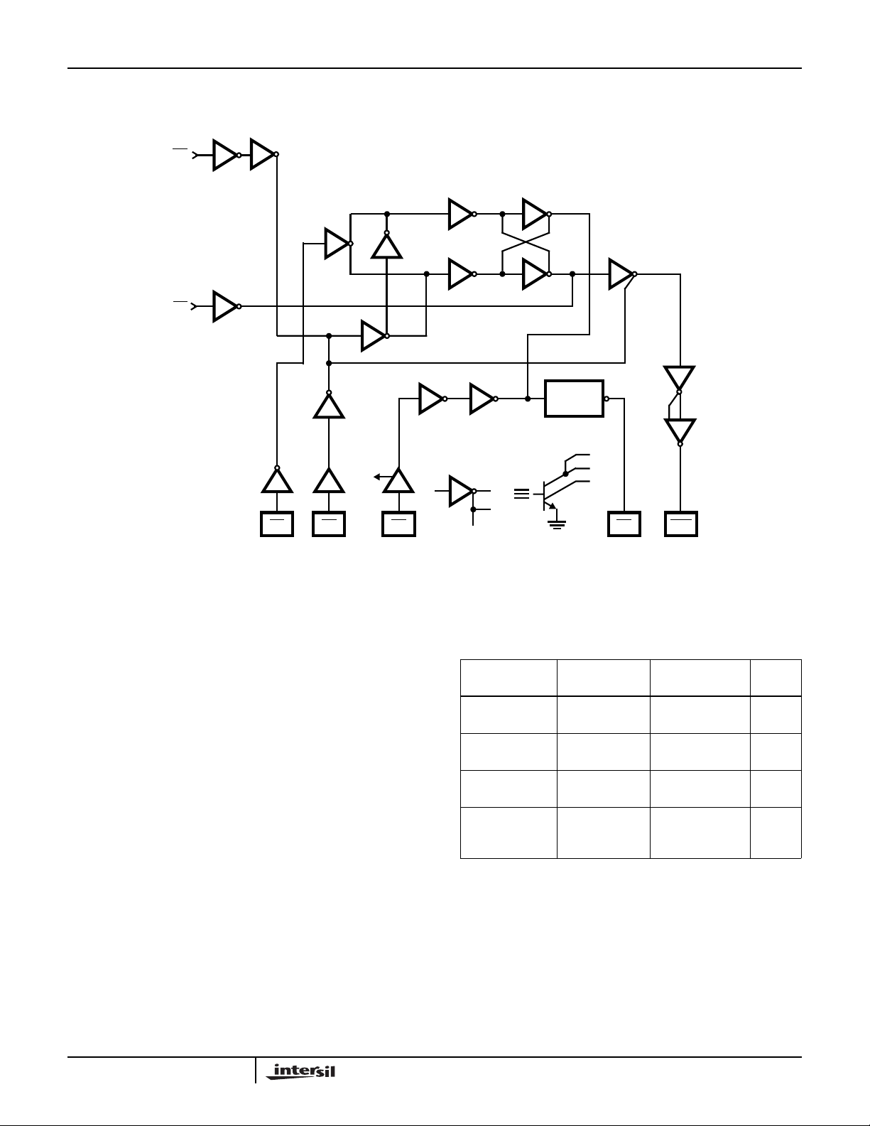
LOGIC GATE SCHEMATIC
2
TTL
TO
STTL
6
4
15
5
10
11 14
TTL
TO
STTL
TO
R
21
C
SCHOTTKY LOGIC
8
97
RELAY
DRIVER
A
B
12
13
STTL
C
B
A
TO
TTL
SHDRDPDRCRS
FIGURE 9. LOGIC NETWORK
Overvoltage Protection and Longitudinal
Current Protection
The SLIC device, in conjunction with an external protection
bridge, will withstand high voltage lightning surges and
power line crosses.
High voltage surge conditions are as specified in Table 1.
The SLIC will withstand longitudinal currents up to a
maximum or 10mA
performance degradation.
RMS
, 5mA
per leg, without any
RMS
TEST
PARAMETER
Longitudinal
Surge
CONDITION
10µs Rise/
1000µs Fall
Metallic Surge 10µs Rise/
1000µs Fall
T/GND
R/GND
50/60Hz Current
T/GND
R/GND
10µs Rise/
1000µs Fall
11 Cycles
Limited to
10A
RMS
TABLE 1.
PERFORMANCE
(MAX) UNITS
±450 (Plastic) V
±450 (Plastic) V
±450 (Plastic) V
315 (Plastic) V
PEAK
PEAK
PEAK
RMS
14

Application Circuit
+5V
HC5503
SYSTEM CONTROLLER
R
5
(NOTE 6)
R
S1
TIP
K
1A
Z1
PRIMARY
PROTECTION
MUST LIMIT
INPUT VOLTAGE
TO LESS THAN
450V
RING
16 18 9 19
C
S1
K
1B
PTC
D
D
2
4
V
BAT
-24V
D
5
R
B1
C
S2
R
S2
K
1
10
RD
2
TIP
TIP FEED
11
D
1
V
BAT
-24V
D
3
12
RING FEED
RING FEED SENSE
4
R
B2
V
BAT
-24V
RING
3
C
5
PD
HC5503
U1
(PINOUT FOR PLCC)
AGNDDGNDBGND-BAT
RCRSSHD
R
3
25
RX
C
28
T
X
6
C
1
26
C
2
V
CC
C
2
52771413
C
6
V
CC
+5V
R
4
3
R
C
4
C
1
CODEC/FILTER
R
1
2
U2
V
V
OUT
IN
NOTES:
6. R5 sets the 2-wire to 4-wire gain. R5 = 150kΩ then A
= 0dB. R5= 75kΩ then A
2-4
= -6.0dB.
2-4
7. Secondary protection diode bridge recommended is a 2A, 200V type.
8. All grounds (AG, BG, and DG) must be applied before VCCor V
. Failure to do so may result in premature failure of the part. If a user wishes
BAT
to run separate grounds off a line card, the AG must be applied first.
9. Application shows Ring Injected Ringing, Balanced or Tip injected configuration may be used.
FIGURE 10. -24V APPLICATION CIRCUIT
Typical Component Values:
C1 = 0.33µF, 20%, 20V.
C2 = 1.0µF, 10%, 20V.
C3 = C4 = 0.47µF, 20%, 30V.
C5, C6= 0.01µF, 30V.
CS1=CS2= 0.1µF, 200V typically,depending on V
RING
and
RS1 = RS2 = 1kΩ, 1%, 1/4W.
R1 = 10kΩ, 1%, 1/4W.
R2 = 24.9kΩ, 1%, 1/4W.
R3 = R5 = 150kΩ, 1%, 1/4W.
R4 = 200kΩ, 1%, 1/4W.
D1, D2, D3, D4, D5 = 1N40007, 100V, 3A.
line length.
Z1 = 250V to 350V transient protection.
R
= RB2 = 150 (1% absolute value).
B1
PTC used as ring generator ballast.
15

HC5503
All Intersil semiconductor products are manufactured, assembled and tested under ISO9000 quality systems certification.
Intersil semiconductor products are sold by description only.Intersil Corporation reserves the right to make changes in circuit design and/or specifications at any time without notice. Accordingly, the reader is cautioned to verify that data sheets are current before placing orders. Information furnished by Intersil is believed to be accurate and
reliable. However, no responsibility is assumed by Intersil or its subsidiaries for its use; nor for any infringements of patents or other rights of third parties which may result
from its use. No license is granted by implication or otherwise under any patent or patent rights of Intersil or its subsidiaries.
For information regarding Intersil Corporation and its products, see web site http://www.intersil.com
Sales Office Headquarters
NORTH AMERICA
Intersil Corporation
P. O. Box 883, Mail Stop 53-204
Melbourne, FL 32902
TEL: (407) 724-7000
FAX: (407) 724-7240
16
EUROPE
Intersil SA
Mercure Center
100, Rue de la Fusee
1130 Brussels, Belgium
TEL: (32) 2.724.2111
FAX: (32) 2.724.22.05
ASIA
Intersil (Taiwan) Ltd.
7F-6, No. 101 Fu Hsing North Road
Taipei, Taiwan
Republic of China
TEL: (886) 2 2716 9310
FAX: (886) 2 2715 3029
 Loading...